US10592033B2 - Pressure sensor, touch substrate and touch display device - Google Patents
Pressure sensor, touch substrate and touch display device Download PDFInfo
- Publication number
- US10592033B2 US10592033B2 US15/552,370 US201715552370A US10592033B2 US 10592033 B2 US10592033 B2 US 10592033B2 US 201715552370 A US201715552370 A US 201715552370A US 10592033 B2 US10592033 B2 US 10592033B2
- Authority
- US
- United States
- Prior art keywords
- substrate
- pressure sensor
- signal lines
- elastic layer
- lines
- Prior art date
- Legal status (The legal status is an assumption and is not a legal conclusion. Google has not performed a legal analysis and makes no representation as to the accuracy of the status listed.)
- Active, expires
Links
Images



Classifications
-
- G—PHYSICS
- G01—MEASURING; TESTING
- G01L—MEASURING FORCE, STRESS, TORQUE, WORK, MECHANICAL POWER, MECHANICAL EFFICIENCY, OR FLUID PRESSURE
- G01L5/00—Apparatus for, or methods of, measuring force, work, mechanical power, or torque, specially adapted for specific purposes
- G01L5/0028—Force sensors associated with force applying means
- G01L5/0038—Force sensors associated with force applying means applying a pushing force
-
- G—PHYSICS
- G06—COMPUTING OR CALCULATING; COUNTING
- G06F—ELECTRIC DIGITAL DATA PROCESSING
- G06F3/00—Input arrangements for transferring data to be processed into a form capable of being handled by the computer; Output arrangements for transferring data from processing unit to output unit, e.g. interface arrangements
- G06F3/01—Input arrangements or combined input and output arrangements for interaction between user and computer
- G06F3/03—Arrangements for converting the position or the displacement of a member into a coded form
- G06F3/041—Digitisers, e.g. for touch screens or touch pads, characterised by the transducing means
- G06F3/0414—Digitisers, e.g. for touch screens or touch pads, characterised by the transducing means using force sensing means to determine a position
-
- G—PHYSICS
- G01—MEASURING; TESTING
- G01L—MEASURING FORCE, STRESS, TORQUE, WORK, MECHANICAL POWER, MECHANICAL EFFICIENCY, OR FLUID PRESSURE
- G01L9/00—Measuring steady of quasi-steady pressure of fluid or fluent solid material by electric or magnetic pressure-sensitive elements; Transmitting or indicating the displacement of mechanical pressure-sensitive elements, used to measure the steady or quasi-steady pressure of a fluid or fluent solid material, by electric or magnetic means
- G01L9/0041—Transmitting or indicating the displacement of flexible diaphragms
- G01L9/0051—Transmitting or indicating the displacement of flexible diaphragms using variations in ohmic resistance
-
- G—PHYSICS
- G01—MEASURING; TESTING
- G01L—MEASURING FORCE, STRESS, TORQUE, WORK, MECHANICAL POWER, MECHANICAL EFFICIENCY, OR FLUID PRESSURE
- G01L9/00—Measuring steady of quasi-steady pressure of fluid or fluent solid material by electric or magnetic pressure-sensitive elements; Transmitting or indicating the displacement of mechanical pressure-sensitive elements, used to measure the steady or quasi-steady pressure of a fluid or fluent solid material, by electric or magnetic means
- G01L9/0041—Transmitting or indicating the displacement of flexible diaphragms
- G01L9/0072—Transmitting or indicating the displacement of flexible diaphragms using variations in capacitance
-
- G—PHYSICS
- G02—OPTICS
- G02F—OPTICAL DEVICES OR ARRANGEMENTS FOR THE CONTROL OF LIGHT BY MODIFICATION OF THE OPTICAL PROPERTIES OF THE MEDIA OF THE ELEMENTS INVOLVED THEREIN; NON-LINEAR OPTICS; FREQUENCY-CHANGING OF LIGHT; OPTICAL LOGIC ELEMENTS; OPTICAL ANALOGUE/DIGITAL CONVERTERS
- G02F1/00—Devices or arrangements for the control of the intensity, colour, phase, polarisation or direction of light arriving from an independent light source, e.g. switching, gating or modulating; Non-linear optics
- G02F1/01—Devices or arrangements for the control of the intensity, colour, phase, polarisation or direction of light arriving from an independent light source, e.g. switching, gating or modulating; Non-linear optics for the control of the intensity, phase, polarisation or colour
- G02F1/13—Devices or arrangements for the control of the intensity, colour, phase, polarisation or direction of light arriving from an independent light source, e.g. switching, gating or modulating; Non-linear optics for the control of the intensity, phase, polarisation or colour based on liquid crystals, e.g. single liquid crystal display cells
- G02F1/133—Constructional arrangements; Operation of liquid crystal cells; Circuit arrangements
- G02F1/136—Liquid crystal cells structurally associated with a semi-conducting layer or substrate, e.g. cells forming part of an integrated circuit
- G02F1/1362—Active matrix addressed cells
- G02F1/136286—Wiring, e.g. gate line, drain line
-
- G—PHYSICS
- G06—COMPUTING OR CALCULATING; COUNTING
- G06F—ELECTRIC DIGITAL DATA PROCESSING
- G06F3/00—Input arrangements for transferring data to be processed into a form capable of being handled by the computer; Output arrangements for transferring data from processing unit to output unit, e.g. interface arrangements
- G06F3/01—Input arrangements or combined input and output arrangements for interaction between user and computer
- G06F3/03—Arrangements for converting the position or the displacement of a member into a coded form
- G06F3/041—Digitisers, e.g. for touch screens or touch pads, characterised by the transducing means
-
- G—PHYSICS
- G06—COMPUTING OR CALCULATING; COUNTING
- G06F—ELECTRIC DIGITAL DATA PROCESSING
- G06F3/00—Input arrangements for transferring data to be processed into a form capable of being handled by the computer; Output arrangements for transferring data from processing unit to output unit, e.g. interface arrangements
- G06F3/01—Input arrangements or combined input and output arrangements for interaction between user and computer
- G06F3/03—Arrangements for converting the position or the displacement of a member into a coded form
- G06F3/041—Digitisers, e.g. for touch screens or touch pads, characterised by the transducing means
- G06F3/0414—Digitisers, e.g. for touch screens or touch pads, characterised by the transducing means using force sensing means to determine a position
- G06F3/04144—Digitisers, e.g. for touch screens or touch pads, characterised by the transducing means using force sensing means to determine a position using an array of force sensing means
-
- G—PHYSICS
- G06—COMPUTING OR CALCULATING; COUNTING
- G06F—ELECTRIC DIGITAL DATA PROCESSING
- G06F3/00—Input arrangements for transferring data to be processed into a form capable of being handled by the computer; Output arrangements for transferring data from processing unit to output unit, e.g. interface arrangements
- G06F3/01—Input arrangements or combined input and output arrangements for interaction between user and computer
- G06F3/03—Arrangements for converting the position or the displacement of a member into a coded form
- G06F3/041—Digitisers, e.g. for touch screens or touch pads, characterised by the transducing means
- G06F3/0414—Digitisers, e.g. for touch screens or touch pads, characterised by the transducing means using force sensing means to determine a position
- G06F3/04146—Digitisers, e.g. for touch screens or touch pads, characterised by the transducing means using force sensing means to determine a position using pressure sensitive conductive elements delivering a boolean signal and located between crossing sensing lines, e.g. located between X and Y sensing line layers
-
- G—PHYSICS
- G06—COMPUTING OR CALCULATING; COUNTING
- G06F—ELECTRIC DIGITAL DATA PROCESSING
- G06F3/00—Input arrangements for transferring data to be processed into a form capable of being handled by the computer; Output arrangements for transferring data from processing unit to output unit, e.g. interface arrangements
- G06F3/01—Input arrangements or combined input and output arrangements for interaction between user and computer
- G06F3/03—Arrangements for converting the position or the displacement of a member into a coded form
- G06F3/041—Digitisers, e.g. for touch screens or touch pads, characterised by the transducing means
- G06F3/047—Digitisers, e.g. for touch screens or touch pads, characterised by the transducing means using sets of wires, e.g. crossed wires
-
- H—ELECTRICITY
- H10—SEMICONDUCTOR DEVICES; ELECTRIC SOLID-STATE DEVICES NOT OTHERWISE PROVIDED FOR
- H10D—INORGANIC ELECTRIC SEMICONDUCTOR DEVICES
- H10D30/00—Field-effect transistors [FET]
- H10D30/60—Insulated-gate field-effect transistors [IGFET]
- H10D30/67—Thin-film transistors [TFT]
- H10D30/6729—Thin-film transistors [TFT] characterised by the electrodes
- H10D30/673—Thin-film transistors [TFT] characterised by the electrodes characterised by the shapes, relative sizes or dispositions of the gate electrodes
-
- H—ELECTRICITY
- H10—SEMICONDUCTOR DEVICES; ELECTRIC SOLID-STATE DEVICES NOT OTHERWISE PROVIDED FOR
- H10D—INORGANIC ELECTRIC SEMICONDUCTOR DEVICES
- H10D30/00—Field-effect transistors [FET]
- H10D30/60—Insulated-gate field-effect transistors [IGFET]
- H10D30/67—Thin-film transistors [TFT]
- H10D30/6729—Thin-film transistors [TFT] characterised by the electrodes
- H10D30/6737—Thin-film transistors [TFT] characterised by the electrodes characterised by the electrode materials
- H10D30/6739—Conductor-insulator-semiconductor electrodes
-
- G—PHYSICS
- G02—OPTICS
- G02F—OPTICAL DEVICES OR ARRANGEMENTS FOR THE CONTROL OF LIGHT BY MODIFICATION OF THE OPTICAL PROPERTIES OF THE MEDIA OF THE ELEMENTS INVOLVED THEREIN; NON-LINEAR OPTICS; FREQUENCY-CHANGING OF LIGHT; OPTICAL LOGIC ELEMENTS; OPTICAL ANALOGUE/DIGITAL CONVERTERS
- G02F1/00—Devices or arrangements for the control of the intensity, colour, phase, polarisation or direction of light arriving from an independent light source, e.g. switching, gating or modulating; Non-linear optics
- G02F1/01—Devices or arrangements for the control of the intensity, colour, phase, polarisation or direction of light arriving from an independent light source, e.g. switching, gating or modulating; Non-linear optics for the control of the intensity, phase, polarisation or colour
- G02F1/13—Devices or arrangements for the control of the intensity, colour, phase, polarisation or direction of light arriving from an independent light source, e.g. switching, gating or modulating; Non-linear optics for the control of the intensity, phase, polarisation or colour based on liquid crystals, e.g. single liquid crystal display cells
- G02F1/133—Constructional arrangements; Operation of liquid crystal cells; Circuit arrangements
- G02F1/136—Liquid crystal cells structurally associated with a semi-conducting layer or substrate, e.g. cells forming part of an integrated circuit
- G02F1/1362—Active matrix addressed cells
- G02F1/136286—Wiring, e.g. gate line, drain line
- G02F1/136295—Materials; Compositions; Manufacture processes
-
- G—PHYSICS
- G06—COMPUTING OR CALCULATING; COUNTING
- G06F—ELECTRIC DIGITAL DATA PROCESSING
- G06F2203/00—Indexing scheme relating to G06F3/00 - G06F3/048
- G06F2203/041—Indexing scheme relating to G06F3/041 - G06F3/045
- G06F2203/04103—Manufacturing, i.e. details related to manufacturing processes specially suited for touch sensitive devices
Definitions
- Embodiments of the present disclosure relate to a pressure sensor, a touch substrate and a touch display device.
- An in cell touch display device and an on cell touch display device are two common touch display devices.
- a touch sensor structure of the in cell touch display device is arranged within a display panel, and a touch sensor structure of the on cell touch display device is arranged outside the display panel and arranged on a substrate which the display panel comprises.
- a touch sensor structure in the touch display device is obtained by forming one or two conductive thin films on the substrate and performing patterning processing on the one or two conductive thin films.
- a pressure sensor, a touch substrate and a touch display device are provided.
- a pressure sensor comprises: an active layer; a gate electrode, which is stacked with the active layer and insulated from the active layer; an elastic layer, which is arranged between the active layer and the gate electrode in a direction perpendicular to the active layer; and a source electrode and a drain electrode, which are spaced from each other and are both electrically connected with the active layer, wherein, in a case that a pressure is applied to the pressure sensor, a thickness of the elastic layer is decreased.
- the thickness of the elastic layer is decreased by at least about 5%.
- the thickness of the elastic layer is about 0.5 micron to 5 microns in a case that the pressure is not applied to the pressure sensor.
- a Young's modulus of the elastic layer is about 0.1 MPa to 10 MPa.
- a material for forming the elastic layer includes at least one or more of rubber, polyurethane, polypropylene, and polyformaldehyde.
- an orthogonal projection of the gate electrode on the elastic layer is substantially located within the elastic layer.
- an orthogonal projection of the active layer on the elastic layer is substantially located within the elastic layer.
- an interlayer insulating layer is arranged between the elastic layer and at least one of the gate electrode and the active layer.
- the pressure sensor further comprises a substrate on which the active layer, the elastic layer, the gate electrode, the source electrode and the drain electrode are formed, wherein, the elastic layer is arranged on a side of the active layer away from the substrate.
- the touch substrate comprises: a base substrate; a plurality of pressure sensors as described above, which are arranged on the base substrate; a plurality of first signal lines spaced from each other, which are arranged on the base substrate and are electrically connected with gate electrodes of the plurality of pressure sensors respectively; a plurality of second signal lines spaced from each other, which are arranged on the base substrate, intersect with the plurality of first signal lines respectively, and are electrically connected with source electrodes of the plurality of pressure sensors respectively; and a plurality of third signal lines spaced from each other, which are arranged on the base substrate, are insulated from the first signal lines and the second signal lines, and are electrically connected with drain electrodes of the plurality of pressure sensors respectively.
- the plurality of third signal lines are parallel with the plurality of second signal lines.
- the elastic layer of each pressure sensor overlaps with at least one of the second signal line adjacent to the pressure sensor and the third signal line adjacent to the pressure sensor.
- the touch display device comprises the touch substrate as described above.
- the touch display device further comprises a plurality of pixel units and a plurality of transistors, wherein the plurality of transistors are respectively connected with the plurality of pixel units.
- the touch display device further comprises: a plurality of data lines spaced from each other, which are arranged on the base substrate which the touch substrate comprises, and are insulated from the first signal lines, the second signal lines and the third signal lines, wherein, source electrodes of the plurality of transistors are respectively connected with the data lines, and gate electrodes of the plurality of transistors are respectively connected with the first signal lines.
- the touch display device further comprises: a plurality of gate lines spaced from each other, which are arranged on the base substrate which the touch substrate comprises, and are insulated from the first signal lines, the second signal lines and the third signal lines, wherein, gate electrodes of the plurality of transistors are respectively connected with the gate lines, and source electrodes of the plurality of transistors are respectively connected with the second signal lines.
- the touch display device further comprises: a plurality of data lines spaced from each other and a plurality of gate lines spaced from each other, wherein, the date lines and the gate lines are both arranged on the base substrate which the touch substrate comprises, and are insulated from the first signal lines, the second signal lines and the third signal lines, gate electrodes of the plurality of transistors are respectively connected with the gate lines, and source electrodes of the plurality of transistors are respectively connected with the data lines.
- the touch display device further comprises: a flexible substrate arranged opposite to the base substrate which the touch substrate comprises, wherein, the pressure sensors which the touch substrate comprises are arranged between the base substrate and the flexible substrate.
- the touch display device further comprises a display panel, wherein, the display panel includes a first substrate and a second substrate which are arranged opposite to each other, and the pressure sensors which the touch substrate comprises are arranged on a side of the first substrate away from the second substrate.
- the pressure sensor, the touch substrate and the touch display device are provided.
- the pressure elastic layer is arranged between the gate electrode and the active layer of the thin film transistor so as to form the pressure sensor, the thickness of the pressure elastic layer is decreased when the thin film transistor is touched, and therefore the change of the pressure signal can be converted into the change of the output signal of the thin film transistor, and by detecting the output signal of the thin film transistor, the amplitude of the touch pressure and/or the touch position can be determined.
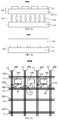
- FIG. 1 is a sectional view of a pressure sensor provided by embodiments of the present disclosure
- FIG. 2 is a sectional view of another pressure sensor provided by the embodiments of the present disclosure.
- FIG. 3 is a sectional view of still another pressure sensor provided by the embodiments of the present disclosure.
- FIGS. 4 a and 4 b are respectively top views of a touch substrate provided by the embodiments of the present disclosure.
- FIGS. 5 a and 5 b are respectively partial sectional views of a touch display device provided by the embodiments of the present disclosure.
- FIGS. 6 a to 6 c are respectively top views of the touch display device provided by the embodiments of the present disclosure.
- Embodiments of the present disclosure provide a pressure sensor, a touch substrate and a touch display device.
- a pressure elastic layer is arranged between a gate electrode and an active layer of a thin film transistor so as to form a pressure sensor, a thickness of the pressure elastic layer is decreased when the thin film transistor is touched, and therefore a change of a pressure signal can be converted into a change of an output signal of the thin film transistor, and by detecting the output signal of the thin film transistor, an amplitude of a touch pressure and/or a touch position can be determined.
- a pressure sensor 10 for example, which is a thin film transistor
- the pressure sensor 10 comprises an active layer 13 , a source electrode 14 a , a drain electrode 14 b , an elastic layer 15 and a gate electrode 16 .
- the source electrode 14 a and the drain electrode 14 b are spaced from each other and are both electrically connected with the active layer 13 .
- the gate electrode 16 is stacked with the active layer 13 and is insulated from the active layer 13 .
- the elastic layer 15 is arranged between the active layer 13 and the gate electrode 16 in a direction perpendicular to the active layer 13 , and for example, the elastic layer 15 is an elastic insulating layer so that the gate electrode 16 and the active layer 13 insulate from each other by the elastic layer 15 ; and the elastic layer 15 is configured to deform in a case that a pressure is applied to the pressure sensor 10 , that is to say, a thickness of the elastic layer 15 is decreased at a position where the pressure is applied to the pressure sensor 10 , and therefore according to a thickness decrease amount of the elastic layer 15 , whether the pressure is applied to the pressure sensor 10 or not and an amplitude of the applied pressure are determined.
- the pressure sensor 10 further comprises a substrate 11 on which the active layer 13 , the elastic layer 15 , the gate electrode 16 , the source electrode 14 a and the drain electrode 14 b are formed, and the elastic layer 15 is arranged on a side of the active layer 13 away from the substrate 11 (as shown in FIG. 1 , the elastic layer 15 is arranged on an upper side of the active layer 13 ).
- the elastic layer 15 is closer to a force applying object (such as a finger), so that the force applying object presses the elastic layer 15 deform more easily.
- the pressure sensor 10 is of a top gate structure, that is to say, the gate electrode 16 is arranged on the side of the active layer 13 away from the substrate 11 .
- the pressure sensor 10 may adopt a bottom gate structure, that is to say, the gate electrode 16 is arranged between the active layer 13 and the substrate 11 .
- the direction perpendicular to the active layer 13 is a direction perpendicular to a main surface of the substrate 11 .
- other structures may further be arranged on the substrate 11 , for example, an insulating layer 12 located between the substrate 11 and the active layer 13 and/or an insulating layer 17 covering the gate electrode 16 , the elastic layer 15 and the active layer 13 are arranged on the substrate 11 .
- the thickness of the elastic layer 15 is decreased, and therefore an output current (namely a current between the source electrode 14 a and the drain electrode 14 b ) of the pressure sensor 10 is increased.
- an output current namely a current between the source electrode 14 a and the drain electrode 14 b
- a thickness change percentage of the elastic layer 15 is at least about 5%.
- an original thickness (a thickness in a case that the pressure is not applied to the pressure sensor 10 ) of the elastic layer 15 is d
- the current between the source electrode 14 a and the drain electrode 14 b is I in a case that the elastic layer 15 is at the original thickness.
- the thickness of the elastic layer 15 is decreased by about 5%, and therefore the thickness of the elastic layer 15 is about (1 ⁇ 5%)d after the thickness is decreased; in this case, the current between the source electrode and the drain electrode is increased by about 5%, and for example, the current after being increased is about (1+5.263%)I.
- the current between the source electrode and the drain electrode is changed by at least about 5%, the change of the current can be reliably detected.
- the thickness of the elastic layer 15 is about 0.5 micron to 5 microns in the case that the pressure is not applied to the pressure sensor 10 .
- Such thickness range is beneficial to detecting the change of the output signal of the pressure sensor 10 . This is because: if the elastic layer 15 is too thick, it needs to apply a high voltage to the gate electrode 16 ; if the elastic layer 15 is too thin, deformation of the elastic layer 15 is not obvious.
- a Young's modulus of a material for forming the elastic layer 15 is about 0.1 MPa to 10 MPa.
- the Young's modulus is a physical parameter representing tensile resistance capacity or pressure resistance capacity of the material within an elastic limit. If the Young's modulus of the elastic layer 15 is lower than about 0.1 MPa, a great pressure is needed to make the elastic layer 15 deform; and if the Young's modulus is greater than about 10 MPa, the elastic layer 15 is too soft, which reduce durability of an electrode (such as the gate electrode 16 ) of the pressure sensor 10 .
- the elastic layer 15 has a restore performance, and in a case that the external force applied to the pressure sensor 10 disappears, the elastic layer 15 automatically restores.
- the elastic layer 15 is made from a macromolecular elastic material, and for example, the material for forming the elastic layer 15 includes at least one or more of rubber, polyurethane, polypropylene, and polyformaldehyde.
- an area of the elastic layer 15 is not limited, and it is only needed that the elastic layer 15 is arranged between the gate electrode 16 and the active layer 13 and is used for reliably detecting the touch pressure.
- an orthogonal projection of the gate electrode 16 on the elastic layer 15 is substantially located within the elastic layer 15 .
- pressure borne by the gate electrode 16 is well transmitted to the elastic layer 15 , thereby being beneficial to guaranteeing sensitiveness of the pressure sensor 10 to the external pressure.
- the elastic layer 15 covers a whole of the source electrode 14 a and the drain electrode 14 b ; or, as shown in FIG. 2 , the elastic layer 15 covers a part of the source electrode 14 a and the drain electrode 14 b.
- an orthogonal projection of the active layer 13 on the elastic layer 15 is substantially located within the elastic layer 15 .
- an interlayer insulating layer 18 a is arranged between the elastic layer 15 and the active layer 13
- another interlayer insulating layer 18 b is arranged between the elastic layer 15 and the gate electrode 16 .
- the interlayer insulating layer 18 a and the interlayer insulating layer 18 b is arranged.
- the active layer 13 for example is made from amorphous silicon, polycrystalline silicon, metal oxide and other semiconductor materials frequently used in the field
- the gate electrode 16 , the source electrode 14 a and the drain electrode 14 b for example are made from aluminum, aluminum neodymium alloy, copper, titanium, molybdenum, molybdenum niobium alloy and other metal materials frequently used in the field
- the substrate 11 for example is a glass substrate, a quartz substrate or a plastic substrate or the like.
- At least one embodiment of the present disclosure further provides a touch substrate 100 , as shown in FIG. 4 a , the touch substrate comprises a base substrate 20 , a plurality of pressure sensors 10 provided by any one of the above embodiments, a plurality of first signal lines 31 , a plurality of second signal lines 32 and a plurality of third signal lines 33 .
- the plurality of pressure sensors 10 are arranged on the base substrate 10 (for example, as shown in FIG.
- the plurality of pressure sensors 10 are spaced from each other); the plurality of first signal lines 31 are arranged on the base substrate 20 and spaced from each other and are electrically connected with gate electrodes 16 of the plurality of pressure sensors 10 respectively (that is to say, each first signal line 31 and a gate electrode 16 of a corresponding pressure sensor 10 are electrically connected, and for example are integrally formed); the plurality of second signal lines 32 are arranged on the base substrate 20 and spaced from each other, intersect with the plurality of first signal lines 31 respectively (that is to say, an extension direction of the second signal lines 32 intersect with an extension direction of the first signal lines 31 ), and are electrically connected with source electrodes 14 a of the plurality of pressure sensors 10 respectively (that is to say, each second signal line 32 and a source electrode 14 a of the corresponding pressure sensor 10 are electrically connected, and for example are integrally formed); the plurality of third signal lines 33 are arranged on the base substrate 20 and spaced from each other, are insulated from the first signal lines 31 and the second
- an insulating layer is arranged between the first signal line 31 and the second signal line 32 in a direction perpendicular to a main surface of the base substrate 20 , so that the first signal line 31 and the second signal line 32 are insulated from each other; similarly, the third signal line 33 is insulated from the first signal line 31 (for example, in a case that the third signal line 33 intersects with the first signal line 31 , as shown in FIG. 4 a ) through an insulating layer; in addition, for example, the base substrate 20 which the touch substrate 100 comprises and the substrate 11 which the pressure sensor 10 comprises is the same substrate.
- the first signal lines 31 and the second signal lines 32 intersect with each other to define a plurality of regions arranged in a matrix manner; in each of the regions, the pressure sensor 10 is arranged, the gate electrode 16 of the pressure sensor 10 is electrically connected with the first signal line 31 defining the region, the source electrode 14 a of the pressure sensor 10 is electrically connected with the second signal line 32 defining the region, and then the drain electrode 14 b of the pressure sensor 10 is connected with the third signal line 33 so as to lead out an output signal of the pressure sensor 10 .
- the touch substrate provided by the embodiments of the present disclosure comprises, but is not limited to, the structure shown in FIG. 4 a.
- the embodiments of the present disclosure provide the touch substrate 100 using the pressure sensor 10 provided by any one of the above embodiments as a touch sensor, in the case that a touch object (such as a finger of a user) touches the touch substrate 100 , the elastic layer 15 in the pressure sensor 10 to which the touching object applies the pressure deforms, and therefore the current output by the third signal line 33 connected with the pressure sensor 10 changes, and according to the change of the current, the touch position is determined. For example, by applying a scanning signal to the first signal lines 31 one by one, the touch position is determined according to the change of the current of the third signal line 33 .
- the touch position can be determined in other manners.
- the plurality of third signal lines 33 are substantially parallel with the plurality of second signal lines 32 .
- the third signal lines 33 and the second signal lines 32 are arranged in a same layer, that is to say, the third signal lines 33 and the second signal lines 32 are formed by performing patterning processing on a same thin film.
- the plurality of third signal lines 33 and the plurality of second signal lines 32 are substantially perpendicular to the first signal lines 31 .
- the elastic layers 15 of the plurality of pressure sensors 10 which the touch substrate comprises are spaced from each other (as shown in FIG. 4 a ), or are continuously and integrally formed.
- the elastic layer 15 of each pressure sensor 10 overlap with at least one of the second signal line 32 adjacent to the pressure sensor 10 and the third signal line 33 adjacent to the pressure sensor 10 .
- the elastic layer 15 of each pressure sensor overlaps with the adjacent second signal line 32 and the adjacent third signal line 33 . Due to the overlapping arrangement, an area of the elastic layer 15 is increased, and therefore it is beneficial to increase an area of the whole pressure sensor.
- At least one embodiment of the present disclosure further provides a touch display device, and the touch display device comprises the touch substrate 100 provided by any one of the above embodiments.
- the touch display device comprises the touch substrate 100 provided by any one of the above embodiments.
- the touch display device is an on cell touch display device.
- the touch display device 1000 provided by at least one embodiment of the present disclosure further comprises a display panel 600 , the display panel 600 includes a first substrate 610 and a second substrate 620 arranged opposite to each other, the first substrate 610 (compared with the second substrate 620 ) is closer to a user when the touch display device 1000 works, and the pressure sensor 10 which the touch substrate 100 comprises is arranged on a side of the first substrate 610 away from the second substrate 620 .
- the first substrate 610 and the second substrate 620 are a glass substrate, a quartz substrate, a plastic substrate or a suitable substrate in any type.
- the first substrate 610 and the base substrate 20 which the touch substrate 100 comprises are the same substrate.
- the display panel 600 is a liquid crystal panel, and in this case, the display panel 600 further includes a liquid crystal layer 630 , as shown in FIG. 5 a .
- the display panel 600 for example is an organic light emitting diode (OLED) display panel or a light emitting diode (LED) display panel or the like.
- the pressure sensor 10 is covered with a flexible layer (not shown in FIG. 5 a ), the flexible layer protects the pressure sensor 10 , and the flexible layer is bent after bearing the touch, and therefore the elastic layer of the pressure sensor 10 correspondingly deforms.
- the flexible layer is made from an organic insulating material.
- the insulating layer 17 which the pressure sensor 10 comprises is the flexible layer.
- the touch display device is an in cell touch display device.
- the touch display device 1000 comprises a flexible substrate 700 arranged opposite to the base substrate 20 , the flexible substrate 700 , the base substrate 20 and the structure located between the flexible substrate 700 and the base substrate 20 form the display panel, and for example, the display panel is the organic light emitting diode (OLED) display panel or the light emitting diode (LED) display panel or the like; the pressure sensor 10 which the touch substrate 100 comprises is arranged between the base substrate 20 and the flexible substrate 700 .
- the flexible substrate 700 deforms in a case of bearing the touch, and therefore the elastic layer of the pressure sensor 10 correspondingly deforms.
- the touch display device 1000 provided by at least one embodiment of the present disclosure further comprises a plurality of pixel units 200 and a plurality of transistors 300 located in the display panel (three pixel units 200 and three transistors 300 are shown in FIGS. 6 a to 6 c ).
- the plurality of pixel units 200 are configured for displaying an image.
- the plurality of transistors 300 are respectively connected with the plurality of pixel units 200 (as shown in FIGS.
- each transistor 300 is connected with one pixel unit 200 ) so as to control a display state of the plurality of pixel units 200 ; each transistor 300 includes a gate electrode 310 , a source electrode 321 and a drain electrode 322 , and the drain electrode 322 of each transistor 300 is connected with a corresponding pixel unit 200 .
- each pixel unit 200 includes a light emitting element, such as an OLED element or an LED element or the like, and in this case, for example, the touch display device 1000 is the OLED touch display device or the LED touch display device or a touch display device actively emitting light; for example, each pixel unit 200 further includes a pixel electrode, and in this case, for example, the touch display device 1000 is the touch liquid crystal display device.
- a light emitting element such as an OLED element or an LED element or the like
- the touch display device 1000 is the OLED touch display device or the LED touch display device or a touch display device actively emitting light
- each pixel unit 200 further includes a pixel electrode, and in this case, for example, the touch display device 1000 is the touch liquid crystal display device.
- the touch display device 1000 provided by at least one embodiment of the present disclosure further comprises a plurality of data lines 400 spaced from each other and a plurality of gate lines 500 spaced from each other, for example, at a position where the data line 400 intersects with the gate line 500 , an insulating layer is arranged between the data line 400 and the gate line 500 , so that the data line 400 is insulated from the gate line 500 .
- the gate electrodes 310 of the plurality of transistors 300 are respectively connected with the gate lines 500 (as shown in drawings, the gate electrode 310 of each transistor 300 is connected with a corresponding gate line 500 ), and each gate line 500 is configured for providing a gate scanning signal for each row of transistors 300 connected with the gate line 500 ;
- the source electrodes 321 of the plurality of transistors 300 are respectively connected with the data lines 400 (as shown in drawings, the source electrode 321 of each transistor 300 is connected with a corresponding data line 400 ), and each data line 400 is configured for providing a data voltage for each column of transistors 300 connected with the data line 400 .
- Insulation arrangement in the embodiments of the present disclosure refers to insulation between a plurality of structures located in a same layer (for example, between the gate lines, between the data lines and between the same kind of signal lines), and also refers to insulation achieved through an insulating layer at intersection positions of structures located in different layers (for example, between the gate lines and the data lines, and between the signal lines and the gate lines or the data lines).
- the first signal lines 31 are substantially parallel with the gate lines 500 , and for example, the first signal lines 31 and the gate lines 500 are arranged in a same layer; for example, an insulating layer is arranged between a layer where the first signal lines 31 and the gate lines 500 are located and a layer where the data lines 400 are located so as to insulate the first signal lines 31 from the data lines 400 .
- the second signal lines 32 and the third signal lines 33 are both substantially parallel with the data lines 400 , for example, the second signal lines 32 , the third signal lines 33 and the data lines 400 are arranged in a same layer.
- the touch display device provided by the embodiments comprises, but is not limited to, these manners.
- a display driving process and a touch driving process of the touch display device 1000 do not interfere with each other, and therefore a display function and a touch function are achieved at the same time or at different times.
- the embodiment as shown in FIG. 6 a can be used for the on cell touch display device and can also be used for the in cell touch display device.
- the gate electrode 16 of the pressure sensor 10 and the gate electrode 310 of the transistor 300 are connected with a same gate line 500 (that is to say, the gate electrode 16 of the pressure sensor 10 and the gate electrode 310 of the transistor 300 are connected with a same first signal line 31 ).
- the data lines 400 and the second signal lines 32 are insulated from each other (for example, the data lines 400 and the second signal lines 32 are arranged in a same layer or are respectively arranged in different layers), the source electrodes 321 of the plurality of transistors 300 are respectively connected with the data lines 400 , and the gate electrodes 310 of the plurality of transistors 300 are respectively connected with the first signal lines 31 .
- the pressure sensors 10 and the transistors 300 connected with the first signal line 31 work at the same time, and therefore the touch function and the display function are achieved at the same time.
- the source electrode 14 a of the pressure sensor 10 and the source electrode 321 of the transistor 300 are connected with a same data line 400 (that is to say, the source electrode 14 a of the pressure sensor 10 and the source electrode 321 of the transistor 300 are connected with a same second signal line 32 ).
- the gate lines 500 and the first signal lines 31 are insulated from each other (for example, the gate lines 500 and the first signal lines 31 are arranged in a same layer or are respectively arranged in different film layers), the gate electrodes 310 of the plurality of transistors 300 are respectively connected with the gate lines 500 , and the source electrodes 321 of the plurality of transistors 300 are respectively connected with the second signal lines 32 .
- the touch function and the display function are achieved at different times. That is to say, during a display period, the gate line 500 applies the gate scanning signal to the transistor 300 connected with the gate line 500 , the data line 400 applies the data voltage to the transistor 300 , and the pressure sensor 10 in the pixel where the transistor 300 is located is in a turned-off state (namely in a non-working state); during a touch period, in a same pixel, the transistor 300 is in a turned-off state, the first signal line 31 applies the gate scanning signal to the gate electrode 16 of the pressure sensor 10 connected with the first signal line 31 and the data line 400 applies a source electrode voltage to the pressure sensor 10 connected with the data line 400 so as to make the pressure sensor 10 in a turned-on state, and therefore the output current of the pressure sensor 10 is output through the third signal line 33 , and the touch can be determined according to the change of the output current.
- FIGS. 6 a to 6 c all can reduce a number of the signal lines, and all can be used in the in cell touch display device.
- each pressure sensor 10 corresponds to one pixel unit 200 ; or, at least one pixel unit is provided between adjacent pressure sensors 10 .
- one pixel unit 200 is provided between the adjacent pressure sensors 10 .
Landscapes
- Engineering & Computer Science (AREA)
- General Engineering & Computer Science (AREA)
- Theoretical Computer Science (AREA)
- Physics & Mathematics (AREA)
- General Physics & Mathematics (AREA)
- Human Computer Interaction (AREA)
- Chemical & Material Sciences (AREA)
- Nonlinear Science (AREA)
- Microelectronics & Electronic Packaging (AREA)
- Mathematical Physics (AREA)
- Crystallography & Structural Chemistry (AREA)
- Analytical Chemistry (AREA)
- Optics & Photonics (AREA)
- Force Measurement Appropriate To Specific Purposes (AREA)
- Devices For Indicating Variable Information By Combining Individual Elements (AREA)
- Liquid Crystal (AREA)
- Electroluminescent Light Sources (AREA)
Applications Claiming Priority (4)
| Application Number | Priority Date | Filing Date | Title |
|---|---|---|---|
| CN201610390259.0 | 2016-06-03 | ||
| CN201610390259.0A CN106066224B (zh) | 2016-06-03 | 2016-06-03 | 压力传感器、触控基板和触控显示装置 |
| CN201610390259 | 2016-06-03 | ||
| PCT/CN2017/074753 WO2017206559A1 (zh) | 2016-06-03 | 2017-02-24 | 压力传感器、触控基板和触控显示装置 |
Publications (2)
| Publication Number | Publication Date |
|---|---|
| US20180188873A1 US20180188873A1 (en) | 2018-07-05 |
| US10592033B2 true US10592033B2 (en) | 2020-03-17 |
Family
ID=57420374
Family Applications (1)
| Application Number | Title | Priority Date | Filing Date |
|---|---|---|---|
| US15/552,370 Active 2037-04-30 US10592033B2 (en) | 2016-06-03 | 2017-02-24 | Pressure sensor, touch substrate and touch display device |
Country Status (4)
| Country | Link |
|---|---|
| US (1) | US10592033B2 (de) |
| EP (1) | EP3467464A4 (de) |
| CN (1) | CN106066224B (de) |
| WO (1) | WO2017206559A1 (de) |
Families Citing this family (9)
| Publication number | Priority date | Publication date | Assignee | Title |
|---|---|---|---|---|
| CN106066224B (zh) | 2016-06-03 | 2018-04-03 | 京东方科技集团股份有限公司 | 压力传感器、触控基板和触控显示装置 |
| CN107145261B (zh) * | 2017-06-30 | 2021-01-05 | 上海天马微电子有限公司 | 一种显示面板和显示装置 |
| CN107168589B (zh) * | 2017-07-20 | 2020-09-18 | 上海天马微电子有限公司 | 一种显示基板及其制作方法、显示面板和显示装置 |
| CN107946369B (zh) * | 2017-11-24 | 2020-10-13 | 合肥鑫晟光电科技有限公司 | 薄膜晶体管、制备方法、检测器件、阵列基板及显示装置 |
| CN110164915A (zh) * | 2018-10-25 | 2019-08-23 | 京东方科技集团股份有限公司 | 显示面板及其制造方法、显示装置 |
| CN109933243A (zh) * | 2019-04-09 | 2019-06-25 | 京东方科技集团股份有限公司 | 触摸屏 |
| WO2021075356A1 (ja) * | 2019-10-15 | 2021-04-22 | パナソニックIpマネジメント株式会社 | 荷重センサ |
| CN115112268B (zh) * | 2021-03-18 | 2025-01-14 | 中国科学院宁波材料技术与工程研究所 | 触觉传感器及其制造方法 |
| CN114251616B (zh) * | 2021-12-27 | 2023-11-24 | 北京印刷学院 | 一种焦点自跟踪的舞台追光灯装置及其使用方法 |
Citations (11)
| Publication number | Priority date | Publication date | Assignee | Title |
|---|---|---|---|---|
| US20060077186A1 (en) * | 2004-09-24 | 2006-04-13 | Samsung Electronics Co., Ltd. | Touch detectable display device and driving method thereof |
| US20090141004A1 (en) * | 2007-12-03 | 2009-06-04 | Semiconductor Energy Laboratory Co., Ltd. | Display device and method for manufacturing the same |
| US20090199648A1 (en) * | 2008-02-13 | 2009-08-13 | Industrial Technology Research Institute | Transistor-type pressure sensor and method for fabricating the same |
| CN102856355A (zh) | 2012-09-04 | 2013-01-02 | 程凯 | 增强型半导体器件 |
| US20130001556A1 (en) | 2011-06-30 | 2013-01-03 | Hon Hai Precision Industry Co., Ltd. | Thin film transistor and press sensing device using the same |
| US20130050126A1 (en) * | 2010-04-21 | 2013-02-28 | Tomohiro Kimura | Display device |
| CN103294317A (zh) | 2013-05-31 | 2013-09-11 | 京东方科技集团股份有限公司 | 一种阵列基板、触控面板及显示装置 |
| CN103608824A (zh) | 2011-05-30 | 2014-02-26 | 3M创新有限公司 | 用于压敏指纹传感器的薄膜层压体 |
| JP2014228454A (ja) | 2013-05-24 | 2014-12-08 | 株式会社フジクラ | 圧力センサ |
| CN105353903A (zh) | 2015-09-30 | 2016-02-24 | 信利光电股份有限公司 | 一种阵列基板、触控显示面板及触控显示装置 |
| CN106066224A (zh) | 2016-06-03 | 2016-11-02 | 京东方科技集团股份有限公司 | 压力传感器、触控基板和触控显示装置 |
-
2016
- 2016-06-03 CN CN201610390259.0A patent/CN106066224B/zh active Active
-
2017
- 2017-02-24 US US15/552,370 patent/US10592033B2/en active Active
- 2017-02-24 EP EP17751591.3A patent/EP3467464A4/de not_active Withdrawn
- 2017-02-24 WO PCT/CN2017/074753 patent/WO2017206559A1/zh not_active Ceased
Patent Citations (13)
| Publication number | Priority date | Publication date | Assignee | Title |
|---|---|---|---|---|
| US20060077186A1 (en) * | 2004-09-24 | 2006-04-13 | Samsung Electronics Co., Ltd. | Touch detectable display device and driving method thereof |
| US20090141004A1 (en) * | 2007-12-03 | 2009-06-04 | Semiconductor Energy Laboratory Co., Ltd. | Display device and method for manufacturing the same |
| US20090199648A1 (en) * | 2008-02-13 | 2009-08-13 | Industrial Technology Research Institute | Transistor-type pressure sensor and method for fabricating the same |
| US20130050126A1 (en) * | 2010-04-21 | 2013-02-28 | Tomohiro Kimura | Display device |
| US20140096622A1 (en) | 2011-05-30 | 2014-04-10 | 3M Innovative Properties Company | Film laminate body for pressure sensitive fingerprint sensor |
| CN103608824A (zh) | 2011-05-30 | 2014-02-26 | 3M创新有限公司 | 用于压敏指纹传感器的薄膜层压体 |
| US20130001556A1 (en) | 2011-06-30 | 2013-01-03 | Hon Hai Precision Industry Co., Ltd. | Thin film transistor and press sensing device using the same |
| CN102856355A (zh) | 2012-09-04 | 2013-01-02 | 程凯 | 增强型半导体器件 |
| JP2014228454A (ja) | 2013-05-24 | 2014-12-08 | 株式会社フジクラ | 圧力センサ |
| CN103294317A (zh) | 2013-05-31 | 2013-09-11 | 京东方科技集团股份有限公司 | 一种阵列基板、触控面板及显示装置 |
| US20150145812A1 (en) | 2013-05-31 | 2015-05-28 | Ordos Yuansheng Optoelectronics Co., Ltd. | Array substrate, touch screen panel and display device |
| CN105353903A (zh) | 2015-09-30 | 2016-02-24 | 信利光电股份有限公司 | 一种阵列基板、触控显示面板及触控显示装置 |
| CN106066224A (zh) | 2016-06-03 | 2016-11-02 | 京东方科技集团股份有限公司 | 压力传感器、触控基板和触控显示装置 |
Non-Patent Citations (2)
| Title |
|---|
| Chinese Office Action dated Aug. 11, 2017. |
| Search Report and Written Opinion dated May 25, 2017 from State Intellectual Property Office of the P.R. China. |
Also Published As
| Publication number | Publication date |
|---|---|
| CN106066224B (zh) | 2018-04-03 |
| EP3467464A1 (de) | 2019-04-10 |
| EP3467464A4 (de) | 2020-02-05 |
| US20180188873A1 (en) | 2018-07-05 |
| CN106066224A (zh) | 2016-11-02 |
| WO2017206559A1 (zh) | 2017-12-07 |
Similar Documents
| Publication | Publication Date | Title |
|---|---|---|
| US10592033B2 (en) | Pressure sensor, touch substrate and touch display device | |
| US11042241B2 (en) | Display device including touch sensor and driving method thereof | |
| KR102418577B1 (ko) | 터치 센서를 가지는 표시 장치 및 그 제조 방법 | |
| KR101274034B1 (ko) | 터치스크린 표시장치 및 이의 제조방법 | |
| US10942594B2 (en) | Integrated electroactive and capacitive touch panel and display device including the same | |
| KR101967290B1 (ko) | 인셀-터치 타입 유기발광다이오드 표시장치 | |
| KR102082425B1 (ko) | 평판표시장치 | |
| KR102261761B1 (ko) | 표시 장치 | |
| US9817503B2 (en) | Thin film transistor substrate and in-cell touch display panel using same | |
| US20150162388A1 (en) | Display device including touch sensor | |
| US10388676B2 (en) | Active matrix substrate and method for producing same, and in-cell touch panel-type display device | |
| US20110267290A1 (en) | Touch screen panel and image display device having the same | |
| US20180101276A1 (en) | Display device and correction method of touch operation | |
| US10248255B2 (en) | Array substrate, touch display panel and method for calculating touch pressure | |
| KR20210041550A (ko) | 터치 센서를 포함하는 표시 장치 및 그 구동 방법 | |
| US20170005110A1 (en) | Array substrate and display device | |
| US10775659B2 (en) | Array substrate, display device and driving method thereof | |
| US10845907B2 (en) | Display panel | |
| JP2021101172A (ja) | 押力センサ | |
| WO2007111044A1 (ja) | 液晶表示装置 | |
| CN112631448A (zh) | 触控显示面板 |
Legal Events
| Date | Code | Title | Description |
|---|---|---|---|
| AS | Assignment |
Owner name: BOE TECHNOLOGY GROUP CO., LTD., CHINA Free format text: ASSIGNMENT OF ASSIGNORS INTEREST;ASSIGNORS:CHENG, HONGFEI;ZHANG, YUXIN;SIGNING DATES FROM 20170731 TO 20170801;REEL/FRAME:043343/0805 |
|
| STPP | Information on status: patent application and granting procedure in general |
Free format text: RESPONSE TO NON-FINAL OFFICE ACTION ENTERED AND FORWARDED TO EXAMINER |
|
| STPP | Information on status: patent application and granting procedure in general |
Free format text: FINAL REJECTION MAILED |
|
| STPP | Information on status: patent application and granting procedure in general |
Free format text: NON FINAL ACTION MAILED |
|
| STPP | Information on status: patent application and granting procedure in general |
Free format text: NOTICE OF ALLOWANCE MAILED -- APPLICATION RECEIVED IN OFFICE OF PUBLICATIONS |
|
| STPP | Information on status: patent application and granting procedure in general |
Free format text: PUBLICATIONS -- ISSUE FEE PAYMENT VERIFIED |
|
| STCF | Information on status: patent grant |
Free format text: PATENTED CASE |
|
| MAFP | Maintenance fee payment |
Free format text: PAYMENT OF MAINTENANCE FEE, 4TH YEAR, LARGE ENTITY (ORIGINAL EVENT CODE: M1551); ENTITY STATUS OF PATENT OWNER: LARGE ENTITY Year of fee payment: 4 |