US4563767A - Method of phase-synchronizing a transit exchange in a digital telecommunication network - Google Patents
Method of phase-synchronizing a transit exchange in a digital telecommunication network Download PDFInfo
- Publication number
- US4563767A US4563767A US06/556,242 US55624283A US4563767A US 4563767 A US4563767 A US 4563767A US 55624283 A US55624283 A US 55624283A US 4563767 A US4563767 A US 4563767A
- Authority
- US
- United States
- Prior art keywords
- signal
- differentiated
- phase
- value
- values
- Prior art date
- Legal status (The legal status is an assumption and is not a legal conclusion. Google has not performed a legal analysis and makes no representation as to the accuracy of the status listed.)
- Expired - Lifetime
Links
- 238000000034 method Methods 0.000 title claims abstract description 9
- 230000001419 dependent effect Effects 0.000 claims description 5
- 230000010354 integration Effects 0.000 claims description 5
- 230000004069 differentiation Effects 0.000 claims description 3
- 230000004044 response Effects 0.000 claims description 2
- 238000004891 communication Methods 0.000 abstract description 3
- 238000010586 diagram Methods 0.000 description 5
- 230000008859 change Effects 0.000 description 4
- 238000001514 detection method Methods 0.000 description 4
- 238000005070 sampling Methods 0.000 description 4
- 230000006870 function Effects 0.000 description 2
- 230000000737 periodic effect Effects 0.000 description 2
- 230000001360 synchronised effect Effects 0.000 description 2
- 230000000694 effects Effects 0.000 description 1
- 238000012544 monitoring process Methods 0.000 description 1
Images

Classifications
-
- H—ELECTRICITY
- H04—ELECTRIC COMMUNICATION TECHNIQUE
- H04L—TRANSMISSION OF DIGITAL INFORMATION, e.g. TELEGRAPHIC COMMUNICATION
- H04L25/00—Baseband systems
- H04L25/38—Synchronous or start-stop systems, e.g. for Baudot code
- H04L25/40—Transmitting circuits; Receiving circuits
-
- H—ELECTRICITY
- H04—ELECTRIC COMMUNICATION TECHNIQUE
- H04J—MULTIPLEX COMMUNICATION
- H04J3/00—Time-division multiplex systems
- H04J3/02—Details
- H04J3/06—Synchronising arrangements
- H04J3/0635—Clock or time synchronisation in a network
- H04J3/0676—Mutual
-
- H—ELECTRICITY
- H04—ELECTRIC COMMUNICATION TECHNIQUE
- H04J—MULTIPLEX COMMUNICATION
- H04J3/00—Time-division multiplex systems
- H04J3/02—Details
- H04J3/06—Synchronising arrangements
- H04J3/0635—Clock or time synchronisation in a network
- H04J3/0685—Clock or time synchronisation in a node; Intranode synchronisation
- H04J3/0691—Synchronisation in a TDM node
Definitions
- the invention relates to a method of and apparatus for phase-synchronising a transit exchange in a digital telecommunication network, including a signal-controlled oscillator, the control signal of which is influenced by the collectively weighted phase difference between the local transit exchange clock and that of the other exchanges.
- a synchronisation of the type mentioned involves each station in the network forming its frequency as a mean value of the frequencies of the incoming links. This is done by measuring the phase differences between incoming link clock signals and the local clock, subsequent to which the phase positions are added or weighted together to provide a control value acting on the clock in the respective exchange via a regulator.
- the phase detector may be analog or digital, although only a digital phase detector is suitable for use in a time multiplex system.
- a phase detector represents a periodic function, i.e. the variation of the faulty signal between zero and the highest deviation corresponding to the phase difference 2 ⁇ is repeated for each 2 ⁇ phase difference. This means that large phase jumps occur just when the phase position exceeds or falls below its measuring range. Even if the sum of the phase positions is kept constant in a network, the individual phase positions can move apart and cause phase jumps. This can result in difficulties when the clock frequency rapidly changes, thus possibly causing new phase jumps. Since the entire network is synchronised, such a phase jump can cause the whole network to hunt.
- An object of the invention is to eliminate this drawback and to provide a method by which phase jumps in the phase detection are avoided. This is accomplished in that the change of phase difference in respect of each of the clock signals of the incoming links is monitored, and if this change exceeds a given limit indicating that a phase jump has taken place, the signal is corrected before it is used for regulation of the oscillator.
- a method of synchronizing the phase of clocks from links from different stations in a transit exchange in a digital telecommunication network including a signal controlled oscillator, the output of which is dependent on collectively weighted phase differences between a local exchange clock and the clocks of the other stations, the method being characterized in that for avoiding a phase jump a signal corresponding to the phase difference is sampled for each of the incoming links thereby producing sampled values. These sampled values are differentiated thereby producing differentiated values. The differentiated values are compared with a limiting value for indicating a phase jump when the limiting value is exceeded.
- a compensation signal having a control signal's highest value but with opposite sign is added to the differentiated value to form a compensated differentiated value.
- the compensated differentiated value is added to the compensated differentiated values corresponding to the other links producing a sum value and the sum value is integrated for obtaining the control signal.
- apparatus for synchronizing the phase of clocks from links from different stations in a transit exchange in a digital communication network including a signal controlled oscillator, the output of which is dependent on collectively weighted phase differences between a local exchange clock and the clocks of the other stations.
- the apparatus includes in accordance with a preferred embodiment phase detectors for sensing the phase difference between the local exchange clock from the signal controlled oscillator and the clocks of each of the incoming links for generating a signal proportional to the phase difference.
- Differentiating circuits are provided for differentiating the phase difference-proportional signal, thereby producing a differentiated signal.
- Compensation means are provided for adding to the differentiated signal in response to the differentiated signal exceeding a given value, a compensation signal with opposite sign and corresponding to the greatest value of a control signal to form a compensated differentiated signal.
- a summing circuit is provided for adding after possible weighting the compensated differentiated signal to the compensated differentiated signals from other links thereby forming a summing result.
- An integration circuit is provided for intergrating the summing result to obtain the control signal.
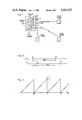
- FIG. 1 schematically illustrates a telecommunication network in which the invention is applied
- FIG. 2 is a time diagram illustrating the clock pulses of an incoming channel and of the local exchange clock
- FIG. 3 illustrates the output signal of a phase detector as a function of the phase difference of the signals fed to the phase detector
- FIG. 4 is a block diagram of an apparatus operating in accordance with the inventive principle.
- FIGS. 5a-e are diagrams illustrating signal values at different points in the circuit according to FIG. 4 for various monitoring times.
- FIG. 1 schematically illustrates a telecommunication network including transit exchanges F1-F4 in connection with each other, via, for example, 32 communication channels.
- the rate of one of these is used to transmit clock signals between the exchanges.
- the phase of the internal clock for example, in the station F1 is in accordance with the average value of the phase difference in respect of each of the incoming channels from stations F2-F4.
- the phase of the incoming clock signals is compared in detectors D2-D4 with the phase of the internal clock K1.
- the signal from the detectors actuates a calculating circuit M1 which in correspondence with the mean or collectively weighted deviation generates a control signal.
- This control signal is supplied to the voltage-controlled oscillator to increase or decrease the frequency through regulator R1 which may consist of a discrete time filter.
- FIG. 2 illustrates the time cycle of the local exchange clock signals and of the incoming clock signals.
- the phase difference ⁇ is measured by the respective phase detector D2-D4, the output signal characteristic of which is illustrated in FIG. 3.
- the characteristic is periodic and has a 0 value at the beginning and a maximum value at the end of each phase difference of 2 ⁇ magnitude.
- FIG. 3 it is easy to understand that a large phase jump occurs just when the phase position falls below or exceeds a measuring range.
- the problem is the same in a network, as even if the sum of the phase positions is kept constant, the individual phase positions may move apart and cause phase jumps. Such phase jumps result in serious disturbances, since the frequency of the clock is rapidly changed and new phase jumps can thereby occur. Since the network is synchronised, such a phase jump can cause hunting in the entire network.
- the effect of the phase jump is eliminated by making a correction for such measured values, the difference of which in relation to a preceding value exceeds a given limit as a result of a phase jump having taken place.
- This is effected in that neither the phase differences nor their sum are to control the oscillator frequency but the phase increments are calculated at each of the sampling moments, and those indicating a phase jump are corrected.
- the phase increments from all the links are summed and this sum is integrated with respect to time, a value being obtained which is equal to the sum of the fictive phase positions of the links. This sum will not have any phase jumps and the system is free from transients caused by diverging phase positions.
- FIG. 4 illustrates an apparatus operating in accordance with the principle mentioned.
- a detection apparatus 1 For cooperation with each of the incoming links there is arranged a detection apparatus 1 of which only what is associated with the link coming from station F2 is shown in detail.
- a digital phase detector 2 compares the clock signal coming from the link, with the local exhcange clock signal, and generates a control signal P proportional to the phase difference.
- This signal is processed in a differentiation circuit 3, which includes a delay circuit 4 and a subtraction circuit 5, and executes a subtraction between two measured values obtained from the digital phase detector at two subsequent samplings.
- the signals obtained from the phase detector are shown in the diagram 5a and the differentiated signals in the diagram 5b at a number of samplings.
- the differentiated signals P are fed to a compensating circuit 6 comprising two comparators 7a and 7b, for comparing the differentiated signal with a positive and a negative threshold value, respectively, corresponding to half of the greatest indication by the phase detector in the example.
- the output signal of the respective comparator closes a contact 8a, 8b connecting a compensation voltage to an addition circuit 9 to which also the differentiated signal is fed directly, such compensation voltage corresponding to the greatest indication by the phase detector, but having opposite sign relative to the respective comparator reference voltage.
- the value of the reference signal is the voltage corresponding to + ⁇ and - ⁇ phase difference
- the value of the compensation voltage corresponds to +2 ⁇ and -2 ⁇ phase difference.
- the values indicated in FIG. 5c are obtained from the adding circuit 9.
- the value of the signal obtained from the sampling point 5 in FIG. 5b, the value and sign change of which signal indicates that a phase jump has taken place, has been changed from what FIG. 5c shows so that the values no longer have any discontinuity.
- the signals from each detecting apparatus 1 are fed to a summing circuit 10 and the sum signal (FIG. 5d) is fed therefrom to an integration circuit 11 comprising a memory 12 and an adding circuit 13, which adds each signal to the preceding signal.
- the resulting signal (FIG. 5e) is subsequently utilized for controlling the frequency of oscillator 15 via a regulator 14, which may consist of a discrete time filter. It is obvious that there is no danger of the network starting to hunt due to phase jumps, since by the differentiation, signal compensation and integration the results of the phase jump have been eliminated. In the example, detection of the phase differences is performed at time intervals of 0.25 s.
- the differentiated phase signal which exceeds a given threshold value and is converted in a compensation circuit corresponding to the circuit 6, is summed with similar signals coming from other links and the sum integrated. This sum signal is then added to the sum of the original phase detection signals from all the links. It should be obvious that such a solution is also within the scope of the invention, as well as the application in a master-slave network where each exchange can sense the phase difference in respect of several exchanges but is only affected by the nearest superordinated station.
Landscapes
- Engineering & Computer Science (AREA)
- Computer Networks & Wireless Communication (AREA)
- Signal Processing (AREA)
- Synchronisation In Digital Transmission Systems (AREA)
- Stabilization Of Oscillater, Synchronisation, Frequency Synthesizers (AREA)
- Time-Division Multiplex Systems (AREA)
- Use Of Switch Circuits For Exchanges And Methods Of Control Of Multiplex Exchanges (AREA)
- Mobile Radio Communication Systems (AREA)
Applications Claiming Priority (2)
| Application Number | Priority Date | Filing Date | Title |
|---|---|---|---|
| SE8201494 | 1982-03-10 | ||
| SE8201494A SE430456B (sv) | 1982-03-10 | 1982-03-10 | Sett och anordning for att fassynkronisera en formedlingstation i ett digitalt telekommunikationsnet |
Publications (1)
| Publication Number | Publication Date |
|---|---|
| US4563767A true US4563767A (en) | 1986-01-07 |
Family
ID=20346223
Family Applications (1)
| Application Number | Title | Priority Date | Filing Date |
|---|---|---|---|
| US06/556,242 Expired - Lifetime US4563767A (en) | 1982-03-10 | 1983-03-01 | Method of phase-synchronizing a transit exchange in a digital telecommunication network |
Country Status (17)
| Country | Link |
|---|---|
| US (1) | US4563767A (it) |
| EP (1) | EP0101713B1 (it) |
| JP (1) | JPS59500346A (it) |
| KR (1) | KR870000074B1 (it) |
| AU (1) | AU564531B2 (it) |
| CA (1) | CA1191210A (it) |
| DE (1) | DE3363869D1 (it) |
| DK (1) | DK161357C (it) |
| EG (1) | EG15936A (it) |
| ES (1) | ES520431A0 (it) |
| FI (1) | FI75703C (it) |
| IE (1) | IE54138B1 (it) |
| IT (1) | IT1201094B (it) |
| MX (1) | MX153259A (it) |
| SE (1) | SE430456B (it) |
| WO (1) | WO1983003175A1 (it) |
| YU (1) | YU56983A (it) |
Cited By (13)
| Publication number | Priority date | Publication date | Assignee | Title |
|---|---|---|---|---|
| US4635249A (en) * | 1985-05-03 | 1987-01-06 | At&T Information Systems Inc. | Glitchless clock signal control circuit for a duplicated system |
| US4807254A (en) * | 1985-08-09 | 1989-02-21 | Nec Corporation | Carrier wave recovery system |
| US4860281A (en) * | 1988-02-29 | 1989-08-22 | Motorola, Inc. | Individual subchannel loopback in the PCM interfaces of a digital telephone exchange with control of the outbound path |
| US4868513A (en) * | 1987-09-11 | 1989-09-19 | Amdahl Corporation | Phase-locked loop with redundant reference input |
| US5060227A (en) * | 1988-02-29 | 1991-10-22 | Motorola, Inc. | Digital telephone switch with simultaneous dual PCM format compatibility |
| US5341405A (en) * | 1991-06-11 | 1994-08-23 | Digital Equipment Corporation | Data recovery apparatus and methods |
| US5384550A (en) * | 1992-09-18 | 1995-01-24 | Rockwell International Corporation | Loop transient response estimator for improved acquisition performance |
| US5408473A (en) * | 1992-03-03 | 1995-04-18 | Digital Equipment Corporation | Method and apparatus for transmission of communication signals over two parallel channels |
| US5412691A (en) * | 1991-06-28 | 1995-05-02 | Digital Equipment Corporation | Method and apparatus for equalization for transmission over a band-limited channel |
| US5450447A (en) * | 1992-09-30 | 1995-09-12 | Rockwell International Corporation | Adaptive variable-gain phase and frequency locked loop for rapid carrier acquisition |
| US5572157A (en) * | 1992-02-24 | 1996-11-05 | Hitachi, Ltd. | Digital phase-looked loop circuit |
| US20080079501A1 (en) * | 2006-09-29 | 2008-04-03 | Hulfachor Ronald B | Technique for switching between input clocks in a phase-locked loop |
| US20080079510A1 (en) * | 2006-09-29 | 2008-04-03 | Seethamraju Srisai R | Programmable phase-locked loop responsive to a selected bandwidth and a selected reference clock signal frequency to adjust circuit characteristics |
Families Citing this family (2)
| Publication number | Priority date | Publication date | Assignee | Title |
|---|---|---|---|---|
| US4736393A (en) * | 1986-04-16 | 1988-04-05 | American Telephone And Telegraph Co., At&T Information Systems, Inc. | Distributed timing control for a distributed digital communication system |
| GB2242800B (en) * | 1990-04-03 | 1993-11-24 | Sony Corp | Digital phase detector arrangements |
Citations (5)
| Publication number | Priority date | Publication date | Assignee | Title |
|---|---|---|---|---|
| US3555194A (en) * | 1967-11-17 | 1971-01-12 | Nippon Electric Co | Interstation synchronization apparatus |
| US3597552A (en) * | 1968-10-25 | 1971-08-03 | Nippon Electric Co | System synchronization system for a time division communication system employing digital control |
| US3862365A (en) * | 1971-11-12 | 1975-01-21 | Nippon Electric Co | Synchronizing system for a plurality of signal transmitters using oscillators of high frequency stability |
| US4075248A (en) * | 1976-09-07 | 1978-02-21 | Domtar Limited | Production of syringealdehyde from hardwood waste pulping liquors |
| US4339817A (en) * | 1979-09-03 | 1982-07-13 | Nippon Electric Co., Ltd. | Clock recovery circuit for burst communications systems |
Family Cites Families (3)
| Publication number | Priority date | Publication date | Assignee | Title |
|---|---|---|---|---|
| JPS50115715A (it) * | 1974-02-22 | 1975-09-10 | ||
| SE398698B (sv) * | 1976-04-27 | 1978-01-09 | Ericsson Telefon Ab L M | Anordning for fassynkronisering av en formedlingsstation i ett digitalt telekommunikationsnet |
| SE7714965L (sv) * | 1977-12-30 | 1979-07-01 | Ericsson Telefon Ab L M | Anordning for att uppretthalla synkronism i ett digitalt telekommunikationsnet |
-
1982
- 1982-03-10 SE SE8201494A patent/SE430456B/sv not_active IP Right Cessation
-
1983
- 1983-03-01 US US06/556,242 patent/US4563767A/en not_active Expired - Lifetime
- 1983-03-01 EP EP83900813A patent/EP0101713B1/en not_active Expired
- 1983-03-01 JP JP58500808A patent/JPS59500346A/ja active Granted
- 1983-03-01 WO PCT/SE1983/000068 patent/WO1983003175A1/en not_active Ceased
- 1983-03-01 IE IE423/83A patent/IE54138B1/en not_active IP Right Cessation
- 1983-03-01 DE DE8383900813T patent/DE3363869D1/de not_active Expired
- 1983-03-01 AU AU12296/83A patent/AU564531B2/en not_active Ceased
- 1983-03-03 MX MX196461A patent/MX153259A/es unknown
- 1983-03-07 KR KR1019830000904A patent/KR870000074B1/ko not_active Expired
- 1983-03-08 CA CA000423083A patent/CA1191210A/en not_active Expired
- 1983-03-08 IT IT19945/83A patent/IT1201094B/it active
- 1983-03-08 EG EG157/83A patent/EG15936A/xx active
- 1983-03-09 YU YU00569/83A patent/YU56983A/xx unknown
- 1983-03-09 ES ES520431A patent/ES520431A0/es active Granted
- 1983-10-25 FI FI833901A patent/FI75703C/sv not_active IP Right Cessation
- 1983-11-09 DK DK513383A patent/DK161357C/da not_active IP Right Cessation
Patent Citations (5)
| Publication number | Priority date | Publication date | Assignee | Title |
|---|---|---|---|---|
| US3555194A (en) * | 1967-11-17 | 1971-01-12 | Nippon Electric Co | Interstation synchronization apparatus |
| US3597552A (en) * | 1968-10-25 | 1971-08-03 | Nippon Electric Co | System synchronization system for a time division communication system employing digital control |
| US3862365A (en) * | 1971-11-12 | 1975-01-21 | Nippon Electric Co | Synchronizing system for a plurality of signal transmitters using oscillators of high frequency stability |
| US4075248A (en) * | 1976-09-07 | 1978-02-21 | Domtar Limited | Production of syringealdehyde from hardwood waste pulping liquors |
| US4339817A (en) * | 1979-09-03 | 1982-07-13 | Nippon Electric Co., Ltd. | Clock recovery circuit for burst communications systems |
Cited By (16)
| Publication number | Priority date | Publication date | Assignee | Title |
|---|---|---|---|---|
| US4635249A (en) * | 1985-05-03 | 1987-01-06 | At&T Information Systems Inc. | Glitchless clock signal control circuit for a duplicated system |
| US4807254A (en) * | 1985-08-09 | 1989-02-21 | Nec Corporation | Carrier wave recovery system |
| US4868513A (en) * | 1987-09-11 | 1989-09-19 | Amdahl Corporation | Phase-locked loop with redundant reference input |
| US4860281A (en) * | 1988-02-29 | 1989-08-22 | Motorola, Inc. | Individual subchannel loopback in the PCM interfaces of a digital telephone exchange with control of the outbound path |
| US5060227A (en) * | 1988-02-29 | 1991-10-22 | Motorola, Inc. | Digital telephone switch with simultaneous dual PCM format compatibility |
| US5341405A (en) * | 1991-06-11 | 1994-08-23 | Digital Equipment Corporation | Data recovery apparatus and methods |
| US5412691A (en) * | 1991-06-28 | 1995-05-02 | Digital Equipment Corporation | Method and apparatus for equalization for transmission over a band-limited channel |
| US5572157A (en) * | 1992-02-24 | 1996-11-05 | Hitachi, Ltd. | Digital phase-looked loop circuit |
| US5841303A (en) * | 1992-02-24 | 1998-11-24 | Hitachi, Ltd. | Digital phase-locked loop circuit |
| US5408473A (en) * | 1992-03-03 | 1995-04-18 | Digital Equipment Corporation | Method and apparatus for transmission of communication signals over two parallel channels |
| US5384550A (en) * | 1992-09-18 | 1995-01-24 | Rockwell International Corporation | Loop transient response estimator for improved acquisition performance |
| US5450447A (en) * | 1992-09-30 | 1995-09-12 | Rockwell International Corporation | Adaptive variable-gain phase and frequency locked loop for rapid carrier acquisition |
| US20080079501A1 (en) * | 2006-09-29 | 2008-04-03 | Hulfachor Ronald B | Technique for switching between input clocks in a phase-locked loop |
| US20080079510A1 (en) * | 2006-09-29 | 2008-04-03 | Seethamraju Srisai R | Programmable phase-locked loop responsive to a selected bandwidth and a selected reference clock signal frequency to adjust circuit characteristics |
| US7405628B2 (en) * | 2006-09-29 | 2008-07-29 | Silicon Laboratories Inc. | Technique for switching between input clocks in a phase-locked loop |
| US7443250B2 (en) | 2006-09-29 | 2008-10-28 | Silicon Laboratories Inc. | Programmable phase-locked loop responsive to a selected bandwidth and a selected reference clock signal frequency to adjust circuit characteristics |
Also Published As
| Publication number | Publication date |
|---|---|
| IE830423L (en) | 1983-09-10 |
| YU56983A (en) | 1986-04-30 |
| AU1229683A (en) | 1983-10-18 |
| EP0101713A1 (en) | 1984-03-07 |
| AU564531B2 (en) | 1987-08-13 |
| DE3363869D1 (en) | 1986-07-10 |
| KR840004633A (ko) | 1984-10-22 |
| FI833901A0 (fi) | 1983-10-25 |
| WO1983003175A1 (en) | 1983-09-15 |
| FI833901A7 (fi) | 1983-10-25 |
| MX153259A (es) | 1986-09-02 |
| JPS59500346A (ja) | 1984-03-01 |
| SE430456B (sv) | 1983-11-14 |
| IE54138B1 (en) | 1989-06-21 |
| DK161357C (da) | 1991-12-02 |
| EG15936A (en) | 1986-12-30 |
| IT1201094B (it) | 1989-01-27 |
| DK513383A (da) | 1983-11-09 |
| SE8201494L (sv) | 1983-09-11 |
| DK161357B (da) | 1991-06-24 |
| IT8319945A0 (it) | 1983-03-08 |
| CA1191210A (en) | 1985-07-30 |
| ES8407275A1 (es) | 1984-08-16 |
| JPH0443480B2 (it) | 1992-07-16 |
| FI75703C (sv) | 1988-07-11 |
| FI75703B (fi) | 1988-03-31 |
| KR870000074B1 (ko) | 1987-02-09 |
| ES520431A0 (es) | 1984-08-16 |
| EP0101713B1 (en) | 1986-06-04 |
| DK513383D0 (da) | 1983-11-09 |
Similar Documents
| Publication | Publication Date | Title |
|---|---|---|
| EP0101713B1 (en) | Method and apparatus for synchronising the phase of a transit exchange in a digital telecommunication network | |
| AU607475B2 (en) | Asynchronous time division communication system | |
| US4855861A (en) | Longitudinal differential protection | |
| FI91820C (fi) | Menetelmä jänniteohjatun oskilaattorin ohjausjännitteen muodostamiseksi vaiheensäätöpiirissä | |
| US6130531A (en) | Phase angle measurement method and system in electric power systems | |
| US3597552A (en) | System synchronization system for a time division communication system employing digital control | |
| US4320516A (en) | Circuit for ascertaining of the phase jitter of digital signals | |
| US11722168B2 (en) | Electrical phase computation using RF media | |
| JP4051840B2 (ja) | 分散されているシステム機器の同期装置 | |
| US5526383A (en) | Network control system for controlling relative errors between network nodes | |
| US4488108A (en) | Phase detector error compensation apparatus | |
| SU810094A3 (ru) | Способ взаимной синхронизации генера-TOPOB TAKTA СТАНции B узлАХ СЕТи СВ зиС ВРЕМЕННыМ уплОТНЕНиЕМ и уСТРОйСТВОдл ЕгО ОСущЕСТВлЕНи | |
| US4358736A (en) | Phase comparison circuit | |
| JP2000507343A (ja) | 電力システムにおける位相角測定方法とシステム | |
| NO156709B (no) | Fremgangsmaate og apparat for aa fasesynkronisere en transittsentral i et digitalt telekommunikasjonsnett. | |
| JP4535288B2 (ja) | 分散制御システム | |
| CA2276815A1 (en) | Clock generator and synchronizing method | |
| JPH06164381A (ja) | Pllの同期はずれ検出回路 | |
| US6904113B2 (en) | Control of phase locked loop during change of synchronization source | |
| JPH01202114A (ja) | サンプリング方式 | |
| SU785792A1 (ru) | Устройство дл измерени и допускового контрол амплитудно- частотных характеристик четырехполюсников | |
| CN121261862A (zh) | 一种用于配网差动保护的传输延时精确测量同步方法和相关装置 | |
| KR100465298B1 (ko) | 사설 교환기의 입력 신호 선택 방법 및 장치 | |
| JP3265152B2 (ja) | 位相同期制御装置 | |
| SU1020995A1 (ru) | Устройство дл автоматической коррекции амплитудно-частотных искажений трактов систем передачи информации |
Legal Events
| Date | Code | Title | Description |
|---|---|---|---|
| AS | Assignment |
Owner name: FIBEG BETEILIGUNGSUESELLSCHAFT MBH MAINZER STRABE Free format text: ASSIGNMENT OF ASSIGNORS INTEREST.;ASSIGNOR:SCHUMANN, FRANZ;REEL/FRAME:004249/0303 Effective date: 19830831 |
|
| AS | Assignment |
Owner name: TELEFONAKTIEBOLAGET L M ERICSSON, S-126 25 STOCKHO Free format text: ASSIGNMENT OF ASSIGNORS INTEREST.;ASSIGNOR:BRANDT, HARALD E.;REEL/FRAME:004268/0446 Effective date: 19830120 Owner name: TELEFONAKTIEBOLAGET L M ERICSSON,SWEDEN Free format text: ASSIGNMENT OF ASSIGNORS INTEREST;ASSIGNOR:BRANDT, HARALD E.;REEL/FRAME:004268/0446 Effective date: 19830120 |
|
| STCF | Information on status: patent grant |
Free format text: PATENTED CASE |
|
| FEPP | Fee payment procedure |
Free format text: PAYOR NUMBER ASSIGNED (ORIGINAL EVENT CODE: ASPN); ENTITY STATUS OF PATENT OWNER: LARGE ENTITY |
|
| FPAY | Fee payment |
Year of fee payment: 4 |
|
| FEPP | Fee payment procedure |
Free format text: PAYER NUMBER DE-ASSIGNED (ORIGINAL EVENT CODE: RMPN); ENTITY STATUS OF PATENT OWNER: LARGE ENTITY Free format text: PAYOR NUMBER ASSIGNED (ORIGINAL EVENT CODE: ASPN); ENTITY STATUS OF PATENT OWNER: LARGE ENTITY |
|
| FPAY | Fee payment |
Year of fee payment: 8 |
|
| FPAY | Fee payment |
Year of fee payment: 12 |