US4725729A - Apparatus for correcting unevenness of light quantity in an optical reproduction system - Google Patents
Apparatus for correcting unevenness of light quantity in an optical reproduction system Download PDFInfo
- Publication number
- US4725729A US4725729A US06/823,937 US82393786A US4725729A US 4725729 A US4725729 A US 4725729A US 82393786 A US82393786 A US 82393786A US 4725729 A US4725729 A US 4725729A
- Authority
- US
- United States
- Prior art keywords
- light
- light quantity
- flux
- projected
- light flux
- Prior art date
- Legal status (The legal status is an assumption and is not a legal conclusion. Google has not performed a legal analysis and makes no representation as to the accuracy of the status listed.)
- Expired - Fee Related
Links
Images

Classifications
-
- H—ELECTRICITY
- H04—ELECTRIC COMMUNICATION TECHNIQUE
- H04N—PICTORIAL COMMUNICATION, e.g. TELEVISION
- H04N1/00—Scanning, transmission or reproduction of documents or the like, e.g. facsimile transmission; Details thereof
- H04N1/04—Scanning arrangements, i.e. arrangements for the displacement of active reading or reproducing elements relative to the original or reproducing medium, or vice versa
- H04N1/19—Scanning arrangements, i.e. arrangements for the displacement of active reading or reproducing elements relative to the original or reproducing medium, or vice versa using multi-element arrays
- H04N1/191—Scanning arrangements, i.e. arrangements for the displacement of active reading or reproducing elements relative to the original or reproducing medium, or vice versa using multi-element arrays the array comprising a one-dimensional [1D] array
- H04N1/192—Simultaneously or substantially simultaneously scanning picture elements on one main scanning line
- H04N1/193—Simultaneously or substantially simultaneously scanning picture elements on one main scanning line using electrically scanned linear arrays, e.g. linear CCD arrays
- H04N1/1935—Optical means for mapping the whole or part of a scanned line onto the array
- H04N1/1937—Optical means for mapping the whole or part of a scanned line onto the array using a reflecting element, e.g. a mirror or a prism
-
- G—PHYSICS
- G02—OPTICS
- G02B—OPTICAL ELEMENTS, SYSTEMS OR APPARATUS
- G02B19/00—Condensers, e.g. light collectors or similar non-imaging optics
- G02B19/0004—Condensers, e.g. light collectors or similar non-imaging optics characterised by the optical means employed
- G02B19/0028—Condensers, e.g. light collectors or similar non-imaging optics characterised by the optical means employed refractive and reflective surfaces, e.g. non-imaging catadioptric systems
-
- G—PHYSICS
- G02—OPTICS
- G02B—OPTICAL ELEMENTS, SYSTEMS OR APPARATUS
- G02B19/00—Condensers, e.g. light collectors or similar non-imaging optics
- G02B19/0033—Condensers, e.g. light collectors or similar non-imaging optics characterised by the use
- G02B19/0076—Condensers, e.g. light collectors or similar non-imaging optics characterised by the use for use with a detector
-
- G—PHYSICS
- G02—OPTICS
- G02B—OPTICAL ELEMENTS, SYSTEMS OR APPARATUS
- G02B5/00—Optical elements other than lenses
- G02B5/005—Diaphragms
-
- H—ELECTRICITY
- H04—ELECTRIC COMMUNICATION TECHNIQUE
- H04N—PICTORIAL COMMUNICATION, e.g. TELEVISION
- H04N1/00—Scanning, transmission or reproduction of documents or the like, e.g. facsimile transmission; Details thereof
- H04N1/024—Details of scanning heads ; Means for illuminating the original
- H04N1/028—Details of scanning heads ; Means for illuminating the original for picture information pick-up
- H04N1/03—Details of scanning heads ; Means for illuminating the original for picture information pick-up with photodetectors arranged in a substantially linear array
-
- H—ELECTRICITY
- H04—ELECTRIC COMMUNICATION TECHNIQUE
- H04N—PICTORIAL COMMUNICATION, e.g. TELEVISION
- H04N2201/00—Indexing scheme relating to scanning, transmission or reproduction of documents or the like, and to details thereof
- H04N2201/024—Indexing scheme relating to scanning, transmission or reproduction of documents or the like, and to details thereof deleted
- H04N2201/02493—Additional optical elements not otherwise provided for, e.g. filters, polarising plates, masks or apertures
Definitions
- the present invention relates to an optical system in a reproduction apparatus for recording a reproduced picture image of an original picture by projecting picture information on the original picture onto a photoelectrical converting elements(s) such as CCD line sensor etc. and basing on its (their) output signal(s) through a focusing optical system, and particularly relates to an apparatus for obtaining a reproduction picture image(s) of uniform picture quality by correcting unevenness in light quantity of a light quantity projected onto the photoelectrical converting element(s).
- Japanese Patent Laid-Open Publication No. 57-87277 there is disclosed an invention titled "A picture reading apparatus".
- Japanese patent laid-Open Publication No. 57-87277 corresponds to Japanese patent application No. 55-162980, which is one of three priority applications upon which U.S. Pat. No. 4,415,934 (entitled Image Reading Apparatus to M. Konishi issued Nov. 15, 1983) relies for its priority claim.
- the invention relates to a reproduction optical system for focusing each of light fluxes which pass through a lens and divided into two by a dome shaped reflection mirror disposed between the lens and its focusing plane by projecting each of the light fluxes onto individually independent line sensors in an apparatus for projecting and focusing picture information on an original picture onto the CCD line sensors disposed on the projecting plane through the lens.
- the apparatus disclosed in the afore-mentioned publication is considered to be adapted that, when picture information on relatively small original pictures such as a micro film or the like is read out, size of each of line sensors is not required to be excessively large, and that adapted to obtain high resolving power.
- the apparatus disclosed in the above described publication is itself considerably useful, however, when the apparatus is actually applied to a picture scanning reproduction apparatus, for example, such as a facsimile or the like, there is found a problem.
- the problem is as follows, that is, in the apparatus between a lens and its projecting image focusing plane a dome shaped mirror is disposed, so that according to a portion of the focusing plane, certain parts of a light flux which transmitted effective diameter (effective part) of the focusing lens are not reflected, that is, only some parts of the light flux can be utilized, which results in generating partial unevenness in light quantity. In consequence there occurs a problem that even in a recorded reproduction picture(s) unevenness in density is also reproduced. Such unevenness in density is an essential fault in reproduction of the photographic original picture of proper gradation required for faithfully reproducing gradation of the original picture. Solution of the afore-mentioned problem is highly desired.
- the present invention by limiting appropriately unevenness of projecting light flux which causes unevenness of light quantity in the focusing plane with an iris or an optical filter, almost uniform light quantity distribution can be obtained in the projecting light focusing plane, and a reproduction picture of high quality having no unevenness can be recorded.
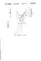
- FIG. 1 is a schematic view showing a reproducing optical system applied to the present invention
- FIG. 2 is a graph representing distribution of light quantity in the focusing plane of the means shown in FIG. 1;
- FIG. 3 is a view diagrammatically showing shape of section of each of light fluxes on the mirror surface
- FIG. 4 is a view showing shape of an iris plate disposed at a position 6 or 7 shown in FIG. 1;
- FIG. 5 is a view showing shape of an opening of an iris plate disposed at a position 8.
- FIG. 1 is a schematic view showing a composition of an embodiment of the present invention.
- An original picture 1 to be reproduced is emitted linearly by an emitting means (not shown), and is fed in the direction vertical to the surface of this sheet.
- a focused image of the emitted portion is projected by a lens 2 to a pair of CCD (charge coupled device) line sensors 4 and 5 disposed at a focusing plane through a dome shaped or triangular roof-shaped mirror 3.
- CCD charge coupled device
- FIG. 2 there is shown a graph representing distribution of light quantity projected on each of positions of the sensor 4. From the graph it can be seen that at the point (a) light quantity is small, but it increases as position separates from the optical axis, and at the vicinity of point (c) it attains the maximum value, then it gradually decreases towards the point (d).
- each of shapes of sections of the respective fluxes at the surface of the dome shaped mirror 3 projected to each of the points (a), (b), (c) and (d) is diagrammatically shown. Shapes of these sections indicate that because of some parts of them being projected on the other reflection surface side of the dome shaped mirror 3, partially broken circular shaped light fluxes which should have been essentially complete circular shaped sections are generated.
- the iris plate for correcting unevenness of light quantity in the apparatus of the present invention can be disposed, if roughly classified, at three positions. That is, those three positions are, as shown in FIG. 1, a position between the original picture 1 and the lens 2 at which an iris plate 6 is provided, a position between the lens 2 and the dome shaped mirror 3 at which an iris plate 7 is disposed, or a position between the dome shaped mirror 3 and the line sensor 4 at which an iris plate 8 is disposed.
- Each of shapes of the respective sections or sectional areas of the fluxes passing through each of those positions is different with one another, so that shapes of those iris plates to be used should be selected basing on the positions at which they are disposed.
- FIG. 4 shows a shape of an opening of the iris plate 6 or 7.
- shapes of sections of the fluxes are symmetrical with respect to the optical axis, so that the shapes of openings of the iris plates 6 and 7 are, of course, symmetrical. Accordingly, at the part of the point (a) or (d) through which a light flux of small light quantity projected thereto, distance between opposite sides of the opening is made larger, and while at the part of the point (b) or (c) through which a light flux of large light quantity projected onto the point, distance between the opposite sides of the opening is made smaller.
- width of the whole light flux (in the upper and down direction in FIG. 1) which passes through the position at which the iris plate 6 is disposed and that of the whole light flux which passes through another position at which the iris plate 7 is disposed are different from each other, accordingly, it is needless to say that the iris plate 7 is made smaller than the iris plate 6 so that the whole size of the opening may be coincided with the width of the light flux. Therefore, these openings become similar figures of different sizes.
- the iris plate 8 disposed between the dome shaped mirror 3 and the line sensor 4 or 5 has an asymmetrical sectional shape resulted from the light flux passing through this part having been already divided into several light fluxes by the dome shaped mirror 3. It is desirable to have a sectional shape as shown in FIG. 5, so that the sectional shape may have an opening size which is inversely proportion to light quantity by corresponding to the graph shown in FIG. 2 which represents distribution of light quantity.
- the iris plate may be disposed at any of the three positions, theoretically it is possible to achieve the object of the present invention, that is, it is possible to obtain evenness in distribution of light quantity projected to the line sensor 4 or 5.
- Such optical filter as mentioned the above is formed as follows, that is, a light shielding pattern having density distribution corresponding to the shape of the opening of the iris plate shown in FIGS. 4 or 5 is formed on a transparent base.
- the light shielding pattern is composed of a pattern which represents high density at positions where distance between each of their opposite sides is smaller, but represents low density at positions where distance between each of their opposite sides is large.
- the most practical means for manufacturing the above described optical filter is to apply a photographical means which utilizes a photographical film(s).
- an object of uniform density distribution for example, a sheet of white paper
- an unexposed photographic film is disposed at the position 9 opposite to the dome shaped mirror 3 at the front plane of the line sensors 4 and 5, and on the film an image of the object is exposed through the lens 2 and the dome shaped mirror 3.
- areas at which received light quantity was large turn out to be high density areas, and areas at which received light quantity was small are found to be low density areas. That is, density distribution thereof is just proportional to the distribution condition of the projected light quantity.
- the original picture 1 is projected onto the line sensor 4 or 5 to focus an image of the original 1 thereon through the lens 2 and the dome shaped mirror 3. Since distribution of the light quantity corresponds to the density distribution of the optical filter, unevenness in both of them is offset, and light fluxes passing through the optical filter incident upon the line sensor with approximately uniform distribution in light quantity. Thus, as same as the case of the iris plate being applied, a picture signal(s) of excellent quality can be output.
- the above mentioned means for manufacturing the optical filter is limited to the only case in which the optical filter made of developed photographic film is disposed at the position 9, i.e., the position between the dome shaped mirror 3 and the line sensor 4 or 5, and an optical filter disposed at the pre-stage of the dome shaped mirror 3 can not be manufactured by the afore-mentioned means. But by disposing the optical filter at any one of the afore-mentioned three positions, the object of the present invention can be achieved, and that even the optical filter can be efficiently applied in practical use as well as the iris plate, if it is disposed between the dome shaped mirror and the line sensor, since it exhibits the most effective function when it is disposed at the position.
- the present invention can be easily practiced merely by disposing the iris plate or the optical filter at an appropriate position in the optical passage;
- the present invention can be easily practiced by the already completed reproduction optical system without adding any large scale of modification thereto.
Landscapes
- Physics & Mathematics (AREA)
- General Physics & Mathematics (AREA)
- Optics & Photonics (AREA)
- Engineering & Computer Science (AREA)
- Multimedia (AREA)
- Signal Processing (AREA)
- Facsimile Scanning Arrangements (AREA)
- Optical Systems Of Projection Type Copiers (AREA)
- Light Sources And Details Of Projection-Printing Devices (AREA)
Applications Claiming Priority (2)
| Application Number | Priority Date | Filing Date | Title |
|---|---|---|---|
| JP60073582A JPS61232763A (ja) | 1985-04-09 | 1985-04-09 | 複写光学系の光量ムラ補正装置 |
| JP60-73582 | 1985-04-09 |
Publications (1)
| Publication Number | Publication Date |
|---|---|
| US4725729A true US4725729A (en) | 1988-02-16 |
Family
ID=13522438
Family Applications (1)
| Application Number | Title | Priority Date | Filing Date |
|---|---|---|---|
| US06/823,937 Expired - Fee Related US4725729A (en) | 1985-04-09 | 1986-01-29 | Apparatus for correcting unevenness of light quantity in an optical reproduction system |
Country Status (3)
| Country | Link |
|---|---|
| US (1) | US4725729A (fr) |
| EP (1) | EP0197251A3 (fr) |
| JP (1) | JPS61232763A (fr) |
Cited By (3)
| Publication number | Priority date | Publication date | Assignee | Title |
|---|---|---|---|---|
| US4823202A (en) * | 1985-08-20 | 1989-04-18 | Dainippon Screen Mfg. Co., Ltd. | Optical beam-splitting arrangements on image side of a lens |
| US5019703A (en) * | 1990-01-25 | 1991-05-28 | Hewlett-Packard Company | Optical scanner with mirror mounted occluding aperture or filter |
| US6023350A (en) * | 1994-11-04 | 2000-02-08 | Noritsu Koki Co., Ltd. | Image reading device for photographic printing |
Families Citing this family (3)
| Publication number | Priority date | Publication date | Assignee | Title |
|---|---|---|---|---|
| FR2696892B1 (fr) * | 1992-10-09 | 1994-12-09 | Thomson Csf | Caméra infrarouge protégée contre les modulations parasites de flux capté. |
| JP4763875B2 (ja) * | 2000-05-01 | 2011-08-31 | 株式会社シグマ | 焦点検出装置 |
| EP1616746B1 (fr) * | 2004-07-15 | 2010-02-24 | Hitachi, Ltd. | Système de commande de véhicule |
Citations (3)
| Publication number | Priority date | Publication date | Assignee | Title |
|---|---|---|---|---|
| US4415934A (en) * | 1980-11-19 | 1983-11-15 | Canon Kabushiki Kaisha | Image reading apparatus |
| US4495422A (en) * | 1981-11-27 | 1985-01-22 | Xerox Corporation | Illumination control for raster input scanners |
| US4547663A (en) * | 1980-12-12 | 1985-10-15 | Canon Kabushiki Kaisha | Focus detecting apparatus with a compensation mask |
Family Cites Families (7)
| Publication number | Priority date | Publication date | Assignee | Title |
|---|---|---|---|---|
| US2298911A (en) * | 1941-04-01 | 1942-10-13 | Rca Corp | Optical system for facsimile transmitters |
| US3469916A (en) * | 1966-10-12 | 1969-09-30 | Dennison Mfg Co | Photographic copying apparatus |
| GB1452490A (en) * | 1973-12-21 | 1976-10-13 | Xerox Corp | Document copying apparatus |
| JPS5417306U (fr) * | 1977-07-05 | 1979-02-03 | ||
| JPS5468107A (en) * | 1977-11-11 | 1979-06-01 | Toshiba Corp | Pick up unit |
| US4321630A (en) * | 1980-09-02 | 1982-03-23 | Xerox Corporation | Linear integrating cavity light collector |
| JPS5787277A (en) * | 1980-11-19 | 1982-05-31 | Canon Inc | Picture reader |
-
1985
- 1985-04-09 JP JP60073582A patent/JPS61232763A/ja active Pending
-
1986
- 1986-01-29 US US06/823,937 patent/US4725729A/en not_active Expired - Fee Related
- 1986-01-31 EP EP86101311A patent/EP0197251A3/fr not_active Withdrawn
Patent Citations (3)
| Publication number | Priority date | Publication date | Assignee | Title |
|---|---|---|---|---|
| US4415934A (en) * | 1980-11-19 | 1983-11-15 | Canon Kabushiki Kaisha | Image reading apparatus |
| US4547663A (en) * | 1980-12-12 | 1985-10-15 | Canon Kabushiki Kaisha | Focus detecting apparatus with a compensation mask |
| US4495422A (en) * | 1981-11-27 | 1985-01-22 | Xerox Corporation | Illumination control for raster input scanners |
Cited By (3)
| Publication number | Priority date | Publication date | Assignee | Title |
|---|---|---|---|---|
| US4823202A (en) * | 1985-08-20 | 1989-04-18 | Dainippon Screen Mfg. Co., Ltd. | Optical beam-splitting arrangements on image side of a lens |
| US5019703A (en) * | 1990-01-25 | 1991-05-28 | Hewlett-Packard Company | Optical scanner with mirror mounted occluding aperture or filter |
| US6023350A (en) * | 1994-11-04 | 2000-02-08 | Noritsu Koki Co., Ltd. | Image reading device for photographic printing |
Also Published As
| Publication number | Publication date |
|---|---|
| EP0197251A3 (fr) | 1987-09-16 |
| JPS61232763A (ja) | 1986-10-17 |
| EP0197251A2 (fr) | 1986-10-15 |
Similar Documents
| Publication | Publication Date | Title |
|---|---|---|
| GB2156624A (en) | A scanning image reproduction system including a plurality of modulated laser beams | |
| JPH08111755A (ja) | 像記録システム | |
| JPS56164312A (en) | Optical deflecting device | |
| US4725729A (en) | Apparatus for correcting unevenness of light quantity in an optical reproduction system | |
| US4178615A (en) | Aperture plate for an exposure head for use in a picture scanning reproducer | |
| US2818465A (en) | Half-tone dot facsimile system | |
| JPS5810713A (ja) | 光ビ−ム分配器 | |
| JP3347167B2 (ja) | 高解像度スキャナ | |
| JPH0220986B2 (fr) | ||
| US5739915A (en) | Electro-optical system for scanning color documents | |
| JPS60642B2 (ja) | 光走査装置 | |
| JPS6276858A (ja) | 透視オリジナルを走査する際のキヤリエ効果を除去する装置 | |
| JPS643244B2 (fr) | ||
| US4587420A (en) | Light beam scanning device for correcting scanning speed | |
| JPH10224609A5 (fr) | ||
| US3536403A (en) | Recording of facsimile signals | |
| US4661858A (en) | Reading apparatus | |
| JPH08132676A (ja) | 画像記録装置 | |
| JPH0614669B2 (ja) | 光ビーム照射装置 | |
| JP2901800B2 (ja) | 画像読取光学装置 | |
| JP3472449B2 (ja) | 走査光学装置 | |
| JPS62128271A (ja) | 画像読み取り装置 | |
| JPS6184620A (ja) | 連続調画像のレ−ザ走査記録装置 | |
| JP2901801B2 (ja) | 画像読取光学装置 | |
| US3585288A (en) | Projection apparatus for use in an image transducing system |
Legal Events
| Date | Code | Title | Description |
|---|---|---|---|
| AS | Assignment |
Owner name: DAINIPPON SCREEN MFG. CO., LTD., 1-1 TENJINKITAMAC Free format text: ASSIGNMENT OF ASSIGNORS INTEREST.;ASSIGNOR:MORIZUMI, YOSHIAKI;REEL/FRAME:004511/0740 Effective date: 19860107 |
|
| FEPP | Fee payment procedure |
Free format text: PAYOR NUMBER ASSIGNED (ORIGINAL EVENT CODE: ASPN); ENTITY STATUS OF PATENT OWNER: LARGE ENTITY |
|
| FPAY | Fee payment |
Year of fee payment: 4 |
|
| FPAY | Fee payment |
Year of fee payment: 8 |
|
| REMI | Maintenance fee reminder mailed | ||
| LAPS | Lapse for failure to pay maintenance fees | ||
| FP | Lapsed due to failure to pay maintenance fee |
Effective date: 20000216 |
|
| STCH | Information on status: patent discontinuation |
Free format text: PATENT EXPIRED DUE TO NONPAYMENT OF MAINTENANCE FEES UNDER 37 CFR 1.362 |