US4733292A - Preparation of fragile devices - Google Patents
Preparation of fragile devices Download PDFInfo
- Publication number
- US4733292A US4733292A US06/893,872 US89387286A US4733292A US 4733292 A US4733292 A US 4733292A US 89387286 A US89387286 A US 89387286A US 4733292 A US4733292 A US 4733292A
- Authority
- US
- United States
- Prior art keywords
- portions
- blank
- fragile
- removing material
- lead
- Prior art date
- Legal status (The legal status is an assumption and is not a legal conclusion. Google has not performed a legal analysis and makes no representation as to the accuracy of the status listed.)
- Expired - Fee Related
Links
Images


Classifications
-
- H—ELECTRICITY
- H10—SEMICONDUCTOR DEVICES; ELECTRIC SOLID-STATE DEVICES NOT OTHERWISE PROVIDED FOR
- H10W—GENERIC PACKAGES, INTERCONNECTIONS, CONNECTORS OR OTHER CONSTRUCTIONAL DETAILS OF DEVICES COVERED BY CLASS H10
- H10W70/00—Package substrates; Interposers; Redistribution layers [RDL]
- H10W70/01—Manufacture or treatment
- H10W70/04—Manufacture or treatment of leadframes
- H10W70/042—Etching
-
- H—ELECTRICITY
- H10—SEMICONDUCTOR DEVICES; ELECTRIC SOLID-STATE DEVICES NOT OTHERWISE PROVIDED FOR
- H10W—GENERIC PACKAGES, INTERCONNECTIONS, CONNECTORS OR OTHER CONSTRUCTIONAL DETAILS OF DEVICES COVERED BY CLASS H10
- H10W70/00—Package substrates; Interposers; Redistribution layers [RDL]
- H10W70/40—Leadframes
- H10W70/421—Shapes or dispositions
-
- H—ELECTRICITY
- H10—SEMICONDUCTOR DEVICES; ELECTRIC SOLID-STATE DEVICES NOT OTHERWISE PROVIDED FOR
- H10W—GENERIC PACKAGES, INTERCONNECTIONS, CONNECTORS OR OTHER CONSTRUCTIONAL DETAILS OF DEVICES COVERED BY CLASS H10
- H10W74/00—Encapsulations, e.g. protective coatings
-
- H—ELECTRICITY
- H10—SEMICONDUCTOR DEVICES; ELECTRIC SOLID-STATE DEVICES NOT OTHERWISE PROVIDED FOR
- H10W—GENERIC PACKAGES, INTERCONNECTIONS, CONNECTORS OR OTHER CONSTRUCTIONAL DETAILS OF DEVICES COVERED BY CLASS H10
- H10W90/00—Package configurations
- H10W90/701—Package configurations characterised by the relative positions of pads or connectors relative to package parts
- H10W90/751—Package configurations characterised by the relative positions of pads or connectors relative to package parts of bond wires
- H10W90/756—Package configurations characterised by the relative positions of pads or connectors relative to package parts of bond wires between a chip and a stacked lead frame, conducting package substrate or heat sink
-
- Y—GENERAL TAGGING OF NEW TECHNOLOGICAL DEVELOPMENTS; GENERAL TAGGING OF CROSS-SECTIONAL TECHNOLOGIES SPANNING OVER SEVERAL SECTIONS OF THE IPC; TECHNICAL SUBJECTS COVERED BY FORMER USPC CROSS-REFERENCE ART COLLECTIONS [XRACs] AND DIGESTS
- Y10—TECHNICAL SUBJECTS COVERED BY FORMER USPC
- Y10T—TECHNICAL SUBJECTS COVERED BY FORMER US CLASSIFICATION
- Y10T29/00—Metal working
- Y10T29/49—Method of mechanical manufacture
- Y10T29/49002—Electrical device making
- Y10T29/49117—Conductor or circuit manufacturing
- Y10T29/49121—Beam lead frame or beam lead device
Definitions
- This invention concerns the preparation of fragile devices by the removal of part of a suitable body of material (by an etching or similar removal process), and relates particularly, though not exclusively, to the formation of lead-frames useful inconnection with the packaging of micro-electronic devices such as integrated circuits.
- circuits in the form of "chips", in which the circuit--containing both passive components, such as conductors, resistors and capacitors, and active components, such as diodes, transistors and other semi-conductor devices--is formed on and in the surface of a fingernail-sized chip of silicon.
- passive components such as conductors, resistors and capacitors
- active components such as diodes, transistors and other semi-conductor devices--is formed on and in the surface of a fingernail-sized chip of silicon.
- the number of connections in and out of the chip may well be at around the hundred mark, but frequently chip designers are pressing for lead counts of a much greater value--possible as high as 400.
- the actual conductors forming these connections have to be only about 1 thou (about 25 microns) wide; this is finer--and much more delicate--than the finest human hair.
- the chip, and its connectors has to be protected, and it is common to encase, or package, the chip, usually in a plastics or ceramic material, to make a larger, stronger article which may relatively safely be handled during the construction of the device of which the chip forms a part.
- One possible end result is the familiar Dual Inline Package (DIP), and oblong object the size of a LEGO brick with conductor "legs" extending downwardly therefrom along either side by which the DIP may be connected onto a Printed Circuit Board (PCB) via holes therein.
- DIP Dual Inline Package
- PCB Printed Circuit Board
- the DIP or FP Flat Pack
- a square object that has its legs on two or all four sides and extending below and then outwardly so that it can sit on the PCB with its legs flush with, and soldered to, the tracks on the board's surface.
- the DIP or FP is preferably achieved by packaging the chip together with what is called a "lead-frame” (a framework of "radially” extending conductive leads that are very fine and fragile on the inside, where the 25 micron connectons are made from them to special pads on the chip itself, but are much coarser, and more robust, on the outside, where the connections are made to the PCB).
- the invention is concerned with the preparation of fragile bodies like this lead-frame.
- the lead-frame blank is masked on either major face so as to define those areas wanted (the connectors, together with a few temporary sections holding the whole together) and unwanted (the spaces between connectors together with the central area where the chip will be), and placed in a bath of chemical etchant material until all the unwanted material has been etched away.
- this other invention suggests a technique whereby most of the thickness of the material over the whole of the lead-frame foil blank's inner area (where the inner connections to the chip will eventually be) is removed from one face to make a generally robust foil with a centrally-located recess defining a much thinner inner section, the recess is filled with some "fixing" material that will both provide support for and hold in position the thin inner section, and further material is then removed from the other face of the blank so as to form the fine inner parts of the lead-frame, these being firmly supported, and held in place, by the "fixing" material filling what was the recess in the foil.
- Such a technique is, of course, applicable to the preparation of many devices in which a fragile area is formed by the removal of a part of a more robust area.
- the invention the subject of this other Application is defined as a method of fabricating a generally planar, sheet-like, device having a first, robust, area and, contiguous therewith, a second, fragile, area to be constructed by removal of some of the material of which the device consists, in which method:
- the preferred technique involves removing material from the blank by an etching process, specifically a chemical etching process.
- the blank is first coated with a masking layer, that covers the areas not to be etched away, and is then contacted with the etch solution.
- the etching occurs only where the blank material is exposed--and at first this is indeed the surface.
- cutting a deeper and deeper "groove" (into the blank material) bounded by "walls" of blank material underlying, and thus protected by, the mask, so the etchant attacks not merely the "floor” of the groove but also these very walls.
- the etch process eats "sideways" into the blank material into the areas beneath the mask, so undercutting the mask.
- the degree of undercut depends on a number of factors, including the detailed crystolographic structure of the blank material and the physical way in which the enchant is allowed to contact the surface; it is common, however, for the unwanted undercut to be about half the depth of the desired etching.
- the net result, though, is that when the mask is removed the fine leads produced by the etching process have quite substantial, wide, bases (where little sideways etching occurred), but have extremely narrow tops (where the maximum undercutting took place).
- the present invention seeks to solve this problem by the extremely simple, but nevertheless very effective, expedient of, as it were, performing the method of this other invention in reverse--that is to say, not of first removing material from one face of the blank to form a recess, and then removing the remainder of the material from the other major face, but instead of first removing material to define the components of the proposed fragile area of the blank, supporting these with fixing material, and then removing the remaining material (to make a recess) from the other face.
- the method to make by etching the fine inner leads of a lead frame it is the wide bases of the leads that are revealed and to which the wire connections may be bonded, rather than the "undercut" upper surfaces.
- the present invention provides a method of fabricating a generally planar, sheet-like, device having a first, robust, area (portion) and, contiguous therewith, a second, fragile, area (portion) to be constructed by removal of some of the material of which the device consists, in which method:
- the method of the invention can, as stated hereinbefore, be applied in the fabrication of numerous types of device, and examples of these are contact sets for electrical switches, and positional sensors. Nevertheless, it is especially suited to the manufacture of lead-frames, as described above, and is for the most part discussed further hereinafter with reference to such a use.
- the inventive method is used in the formation of a generally planar (that is to say, flat), sheet-like, device, and starts with a corresponding generally planar, sheet-like, blank.
- This blank is a sheet, or foil, of material--thus, an article having an area (and length and breadth dimensions) large relative to its thickness, and so has two major faces (the two "sides" of the sheet).
- the material of which the blank is constituted naturally depends upon the nature of the device to be made.
- the material must be an electrical conductor, especially one that is sufficiently malleable to allow itself to be shaped by a bending operation (subsequent to the method of the invention the robust area of the blank will be made into the "legs" of the package, and will need to be bent--and perhaps re-bent--out of the sheet plane and into the correct shape).
- Typical lead-frame materials are made of a suitable metal; nickel-iron alloys of the KOVAR or INVAR type are very suitable, as are copper and copper-based alloys such as beryllium-copper, phosphor bronze (an alloy of tin and copper with up to 0.5 wt % phosphorus) and copper-iron-phosphorus alloys like OLIN 194.
- the device to be fabricated is one having a first area that is robust and--contiguous therewith (and probably wholely surrounded thereby)--a second area that is fragile.
- the two terms "robust” and “fragile” are used in a fairly relative sense--the “fragile” area is one that is significantly less robust than the robust area, and vice versa--though where a lead-frame is concerned the "robust” area ends up as the "legs" of the final package, tough enough to withstand handling, while the "fragile” area ends up as extremely fine conductors rather more delicate than human hair.
- the method of the invention involves removing material from the second area of the blank (and so making that area fragile). Naturally, the distribution of this removal--where, and how much, material is removed--depends the type of device. For a lead-frame, however, there are two distinct classes of material to be removed. One is material removed simply to "thin" the sheet over the whole of the defined, second, area, so that it becomes more suitable for forming into the inner leads of the lead-frame. The other is material removed from between those portions that are to be the leads, so separating each lead from its neighbours.
- the between-lea blank material is removed from one of the blank's major faces, so leaving the formed leads flush with this major face, and standing proud from the remaining "thickness" of the blank (which therefore constitutes a base carrying the formed leads), while in the second stage that base is removed from the other major face, so ending with the leads in this area having a depth equal to roughly half the blank's original thickness.
- Removal of material from the blank is accomplished by any technique suited to the intended device.
- the methods of removal include particle ablation and laser trimming, but--especially for lead-frames--chemical etching is the preferred technique.
- the nature of the etchant will be chosen to fit the blank material; the methods are well known in the Art, and need no detailed comment here--though it may be useful simply to note that nickel iron alloys can best be etched by ferric chloride/hydrochloric acid mixtures, or nitric acid-based materials, while copper and its alloys are preferably dealt with using either ferric chloride or ammoniacal cupric chloride (REGENEX, for instance).
- etching has to be done selectively--some areas are to be removed, some not--and a convenient way to arrange this is to "mask" the areas not to be etched with a protective coating that is unaffected by the etchant to be employed.
- a degree of "undercutting" of the mask is, unfortunately, inevitable, and is the greater as the depth of the etching increases--this masking ensures that only the unmasked, exposed, areas are etched away.
- material is removed from the second area of the blank (that area destined to become the fragile area of the device), to leave the intended fragile components upstanding from, and supported by, a base constituted by second area blank material that has not been removed.
- a base constituted by second area blank material that has not been removed.
- the second area of the blank it is, of course, possible to remove material from the first area (the area destined to become the robust area of the device).
- the robust area end up as leads the outer part of which make the legs of the final package, so that somewhere along the way there must be removed from the blank's robust area all the material between those portions destined to be these leads. At least some of this surplus material can, then, be removed at the same time as the second area is thinned (when using a through-mask etching technique this is arranged quite simply by so designing the mask that the "between-leg" portions remain exposed).
- the between-leg portions are consequently subjected to the same thinning as that effected to the second area, and this is in fact particularly advantageous because (as described further below) it greatly reduces the degree of undercutting of these leg portions as compared with a process wherein all of the depth of the between-leg portions is removed at one go.
- the method of the invention results in the intended fragile components being upstanding from a base.
- the material forming this base will, in the second stage, be removed to leave the fragile components free, so forming the final, fragile area--which, in a lead-frame, is the assembly of inner leads.
- this final form is so fragile it is desirable to support the whole area before the second stage removal is effected, and this is done, in the method of the invention, by filling the gaps between the upstanding fragile components with a fixing material that will, as required, support and fix them in place.
- This fixing material can, naturally, be any appropriate to the circumstances--and, where it is not to be removed after the second stage material removal has occurred, but is to stay as a part of the final device (as is preferred where the device is a lead-frame), this fixing material will also be appropriate to the type of device.
- a lead-frame device is to be packaged with an electrically-insulating packaging material; conventional packaging materials are plastics (such as silica-filled epoxies like POLYSET 410B and NITTO HC10 type 2) and ceramics (such as alumina and beryllia), and clearly the fixing material should be compatible with the packaging material.
- Fixing materials compatible with one or other plastics packaging material are generally the thermosetting resins, specifically the epoxies (such as those named above) while those compatible with one or other ceramics packaging material are generally glasses and glass-ceramics.
- the actual mode of emplacement of the fixing material may be whatever is appropriate.
- a fixing material that is a polymerised plastics might be "injected” or “squeezed” into place in the form of a pasty but flowable pre-polymer mixture (the final polymerisation then taking place in situ); a thermoplastics fixing material might even be "melted” into place.
- a glassy fixing material might likewise be applied, in an un-fired form, and then fired in situ.
- the fixing material is a glass-like lithium alumina silicate, and is deposited in a glassy state and fired in situ to convert it to a glass-ceramic state.
- the fixing material either may be removed at some later stage or may be left in place serving some useful function.
- the material constituting the supporting base of the fragile components is removed from the other major face.
- the removal technique may be any appropriate, as described above.
- blank material can be removed not only from the second area but also from the first area. For example, to make a lead-frame half the thickness of first area material in the between-leg portions is removed (from one major face) in the first stage, and the rest--so separating the "legs" one from another--is removed (from the other major face) in the second stage.
- the device Having removed blank material in the second area both from one major face, and then, after supporting the formed fragile components, from the other major face, the device is complete. lf it is a lead-frame, for example, it can then be used--a chip can be mounted in the centre of the second, fragile, area surrounded by the free ends of the fine inner leads (this central portion will normally have been removed, either during the etching process or by some appropriate alternative method, perhaps as a preliminary measure), these leads can be connected (by wire-bonding, perhaps) to the relevant chip pads, the whole may then be encased in some suitable protector material (often by placing it in a small "box” sealed with a separate lid), but with the remains of the robust blank area--the "leg” portions--projecting therefrom and ready to be bent or otherwise mechanically shaped into the desired "leg” form.
- a lead-frame for example, it can then be used--a chip can be mounted in the centre of the second, fragile, area surrounded by the free ends of the fine inner leads
- the lead-frame may be incorporated within an empty, chip-less open-top package (so that at some subsequent time the chip may be inserted into place and its pads connected up to the inner leads, and a lid attached and sealed shut).
- the process of making such a device is described hereinafter in more detail with reference to the accompanying Drawings and the Examples.
- the lead-frame as first constructed commonly has integrated therewith a whole series of strengthening and retaining members (some of which may be of a plastics, or other non-conducting substance, that is laid in place after the first face treatment but before the second face treatment), together with a series of test points conductively connected to the "leg" portions; some of these extra features of the lead-frame are removed once the completed chip-containing package has been made, while others are removed after the package and its contents have been tested.
- a whole series of strengthening and retaining members some of which may be of a plastics, or other non-conducting substance, that is laid in place after the first face treatment but before the second face treatment
- the invention extends, of course, to a device, particularly a lead-frame, whenever fabricated by the method of the invention.
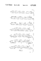
- FIGS. 1A, B, C and D form a sequence of perspective, diagrammatic, views showing symbolically the application of the method of the invention
- FIGS. 2A, B and C form another sequence of perspective, diagrammatic, views showing the various stages in the application of the inventive method to the fabrication of a leadframe.
- FIGS. 3A, B and C show three "plan" views of three leadframe layouts before actual use
- FIGS. 4A, B and C show respectively end elevation see-through, perspective and top-plan see-through views of a DIP employing a leadframe fabricated according to the invention.
- FIGS. 5A to G form a sequence of sectional, diagrammatic, views showing symbolically the application of the method of the invention.
- the starting point is a blank (10)--a sheet of the appropriate material (in a leadframe this would be a conductive metal such as NILO K).
- Blank material is removed, through the mask, to roughly half the blank's depth. Undercutting (as 19) takes place.
- FIGS. 1A, B, C and D series The sequence of operations illustrated by the FIGS. 1A, B, C and D series is generally as follows:
- Blank material is then removed, through the mask, to a depth of roughly half the blank's thickness, so forming a recess (12) in the upper surface, and this recess is then filled with sufficient fixing material 13 to support both the fragile area formed in the final stage, and the immediate surrounds thereof.
- Blank material is then removed, through this second mask, right through to the fixing-material-filled recess 12, so forming the desired fragile area 15 supported by the fixing material 13.
- FIGS. 2A, B and C are a series of perspective views from above (A and B) and from below (C) showing various stages in the formation of a leadframe.
- FIG. 2A depicts the stage after removal of blank material from one major surface so as to define the fragile inner leads (as 25). At the same time, there is removed half the thickness of the blank material elsewhere--the between-leg portion--so as to form in part the outer leads/legs (as 22) of the desired leadframe.
- FIG. 2B there can be seen in place the fixing material (23), which takes the form of a square "ring" of material moulded snugly over the inner leads and leaving a chip-sized central area (24) unfilled.
- FIG. 2C shows from below (as viewed) the leadframe after the remaining unwanted blank material has been removed. From this Figure it will be clear how the fragile inner leads 25 are safely supported by the ring of fixing material 23 while the outer leads 22 now stand free, and support themselves.
- FIGS. 3A, B and C are top plan views of three different lead frames. That of FIG. 3A corresponds to the leadframe of FIG. 2C, that of FIG. 3B relates to a yet more realistic leadframe, while that of FIG. 3C is a slightly enlarged view of a real leadframe.
- the leadframe of FIG. 3B is a four-sided device with 13 leads (as 31) a side (making 52 leads in all). Each lead has a fine, fragile, inner portion (as 31i) and a relatively robust outer portion (as 31o). Within the general area of the inner leads 31i there is a square ring-like lead support (of lead fixing material) whose inner edge is defined by the inner tips of the leads and whose outer edge is shown by the perimeter line (32). Further out from this perimeter is a line (33) indicating where the boundary of the package, forming the desired flat pack, will lie, and just beyond this is a first lead support ring (34) of a nonconductive plastics.
- the preparation of the leadframe of FIG. 3B is as follows. First, from one major side of a blank, there is removed, to half the depth of the blank, all the material between both the inner leads and the outer leads/legs, save for the outer ring 36. Next, the fixing-material inner ring (like 23 in FIG. 3A) is placed in position. Then, all the rest of the blank material between the outer leads/legs, and all the remaining material within the recess periphery (as defined by line 32) is removed from the other side. The finished lead-frame may then be attached to the material which serves as the base of the flat pack. Finally, after possibly bending the leads into the shape required for use, the two support rings 34, 35 are placed in position.
- a chip may be mounted and connected up to the leadframe, the outer blank material ring 36 may be cut off, and the correct working of the chip tested by signals and power sent in and out via the test pads 37; a protective covering may be added; and finally the leads may be cut just outside the first support ring 34 and bent (if not already done) into the required shape for use.
- FIG. 3C shows, slightly enlarged, the lead layout of a real leadframe. It is comparable to FIG. 3B without the latter's two non-conductive support rings, but has 50 leads a side (making 200 leads in all).
- FIGS. 4A, B and C shows various views of a simple Dual Inline Package using a leadframe fabricated in accordance with the invention.
- FIG. 4B gives a general, perspective view from above, while FIGS. 4A and B are respectively a see-through end elevation and a see-through top plan. From these two see-through views it will be apparent that the leadframe has 12 leads (41, 6 on each of the two opposed long sides) that each have a fragile inner portion (41i) and a robust outer portion (41o).
- the inner portions 41i are supported by a "slab" (42) of fixing material, and mounted on that, and connected by wires (as 43) to the inner portions 41i, is the chip (44).
- the whole is encased in a protective package (45), with the ends of the lead outer portions 41o projecting therefrom to form legs.
- a 0.1 mm sheet of NILO K (an alloy of 54 wt % iron, 29 wt % nickel and 17 wt % cobalt) was cut to size, pierced with the requisite tooling/locating apertures, and then vapour degreased to remove its oily protective coating. The surface was then de-oxidised and slightly roughened (abraded) by passing it through a conventional pumice jet scrubber.
- a 0.025 mm layer of a UV-sensitive photo-resist (Dupont's RISTON, a polyvinyl-glycidyl acrylate) was applied to each side of the blank.
- the coated blank was then located in an imager (a Dupont PC Printer Lightbox), and exposed for a suitable intensity/time to UV light through an appropriate artwork master mask, causing partial polymeration of the unshielded resist layer areas.
- imager a Dupont PC Printer Lightbox
- CHLOROTHENE a trichloroethane-based solvent
- the thus-masked blank was then spray etched, using a conventional ferric chloride etchant at 30° C. for sufficient time (a few minutes) to allow the etchant to penetrate about 0.05 mm--half the blank thickness--into the blank material. After washing, the remaining resist was then removed by passing the blank through a bath of SYNSTRYP solvent (based on dichloromethane). At this stage the blank had the complete lead pattern--both the larger outer leads and the very much finer inner leads--etched on one side to a depth halfway through the material.
- a "furnace oxide” coating was then formed on the blank surface by heating the blank in nitrogen with some oxygen in a furnace to around 900° C. over a period of half an hour. Then, using a graphite frame to locate and contain it, a finely powdered lithium aluminosilicate glass was applied to the half-etched fine inner lead area of the blank and fixed into place by fusing in a furnace to about 900° C. In this way the glass flowed around, and "encapsulated", the fine leads.
- the techniques described in Stage 2 above were used to form a photoresist coating on the non-glassed surface, convert this into an appropriate etch-resistant mask (the glassed surface was additionally given an etch-resistant coating of Robertsons Chemicals' Resist 1993, an air-drying liquid resist), etch away the unwanted blank material (so defining the "bottom” half of the large outer leads, and removing all the material in the area "underneath" the fine inner leads), and remove the residue of the photoresist coating.
- the result was the desired leadframe, having large, self-supporting outer leads having a depth equal to that of the original blank and being integral with the glass-supported fine inner leads having half that depth.
Landscapes
- Lead Frames For Integrated Circuits (AREA)
Applications Claiming Priority (2)
| Application Number | Priority Date | Filing Date | Title |
|---|---|---|---|
| GB08519710A GB2178895B (en) | 1985-08-06 | 1985-08-06 | Improved preparation of fragile devices |
| GB8519710 | 1985-08-06 |
Publications (1)
| Publication Number | Publication Date |
|---|---|
| US4733292A true US4733292A (en) | 1988-03-22 |
Family
ID=10583374
Family Applications (1)
| Application Number | Title | Priority Date | Filing Date |
|---|---|---|---|
| US06/893,872 Expired - Fee Related US4733292A (en) | 1985-08-06 | 1986-08-06 | Preparation of fragile devices |
Country Status (4)
| Country | Link |
|---|---|
| US (1) | US4733292A (fr) |
| EP (1) | EP0212890A3 (fr) |
| JP (1) | JPS6290955A (fr) |
| GB (1) | GB2178895B (fr) |
Cited By (29)
| Publication number | Priority date | Publication date | Assignee | Title |
|---|---|---|---|---|
| WO1989000346A1 (fr) * | 1987-07-01 | 1989-01-12 | Western Digital Corporation | Interconnexion crenelee en plastique galvanise pour composants electriques |
| US4919857A (en) * | 1987-03-11 | 1990-04-24 | Tetsuya Hojyo | Method of molding a pin holder on a lead frame |
| US4987475A (en) * | 1988-02-29 | 1991-01-22 | Digital Equipment Corporation | Alignment of leads for ceramic integrated circuit packages |
| US4999700A (en) * | 1989-04-20 | 1991-03-12 | Honeywell Inc. | Package to board variable pitch tab |
| US5009744A (en) * | 1987-08-10 | 1991-04-23 | Murata Manufacturing Co., Ltd. | Method of manufacturing laminated ceramic electronic component |
| US5023700A (en) * | 1988-06-17 | 1991-06-11 | Ngk Insulators, Ltd. | Minutely patterned structure |
| US5034591A (en) * | 1988-03-22 | 1991-07-23 | Amdahl Corporation | Tape automated bonding leads having a stiffener and a method of bonding with same |
| US5069626A (en) * | 1987-07-01 | 1991-12-03 | Western Digital Corporation | Plated plastic castellated interconnect for electrical components |
| US5194698A (en) * | 1990-09-11 | 1993-03-16 | Hughes Aircraft Company | Apparatus and method using a permanent mandrel for manufacture of electrical circuitry |
| US5233220A (en) * | 1989-06-30 | 1993-08-03 | Texas Instruments Incorporated | Balanced capacitance lead frame for integrated circuits and integrated circuit device with separate conductive layer |
| US5253415A (en) * | 1990-03-20 | 1993-10-19 | Die Tech, Inc. | Method of making an integrated circuit substrate lead assembly |
| US5270570A (en) * | 1988-10-10 | 1993-12-14 | Lsi Logic Products Gmbh | Lead frame for a multiplicity of terminals |
| US5286680A (en) * | 1988-12-07 | 1994-02-15 | Tribotech | Semiconductor die packages having lead support frame |
| US5400219A (en) * | 1992-09-02 | 1995-03-21 | Eastman Kodak Company | Tape automated bonding for electrically connecting semiconductor chips to substrates |
| US5454905A (en) * | 1994-08-09 | 1995-10-03 | National Semiconductor Corporation | Method for manufacturing fine pitch lead frame |
| US5466967A (en) * | 1988-10-10 | 1995-11-14 | Lsi Logic Products Gmbh | Lead frame for a multiplicity of terminals |
| US5512780A (en) * | 1994-09-09 | 1996-04-30 | Sun Microsystems, Inc. | Inorganic chip-to-package interconnection circuit |
| US5619065A (en) * | 1991-09-11 | 1997-04-08 | Gold Star Electron Co., Ltd. | Semiconductor package and method for assembling the same |
| US5633205A (en) * | 1994-08-11 | 1997-05-27 | Shinko Electric Industries Co., Ltd. | Lead frame and process of producing such a frame |
| US5683943A (en) * | 1994-06-14 | 1997-11-04 | Dai Nippon Printing Co., Ltd. | Process for etching a semiconductor lead frame |
| US5817544A (en) * | 1996-01-16 | 1998-10-06 | Olin Corporation | Enhanced wire-bondable leadframe |
| US5840599A (en) * | 1989-06-30 | 1998-11-24 | Texas Instruments Incorporated | Process of packaging an integrated circuit with a conductive material between a lead frame and the face of the circuit |
| EP0857355A4 (fr) * | 1996-08-28 | 1999-06-09 | Motorola Inc | Conditionnement verre/metal et son procede de fabrication |
| US5945732A (en) * | 1997-03-12 | 1999-08-31 | Staktek Corporation | Apparatus and method of manufacturing a warp resistant thermally conductive integrated circuit package |
| US6008068A (en) * | 1994-06-14 | 1999-12-28 | Dai Nippon Printing Co., Ltd. | Process for etching a semiconductor lead frame |
| US6007729A (en) * | 1996-10-09 | 1999-12-28 | Texas Instruments Incorporated | Carrier tape and manufacturing method of said carrier tape |
| US6184140B1 (en) * | 1996-12-13 | 2001-02-06 | Tessera, Inc. | Methods of making microelectronic packages utilizing coining |
| US20100264408A1 (en) * | 2007-11-20 | 2010-10-21 | Cambridge Display Technology Ltd. | Organic Thin Film Transistors, Active Matrix Organic Optical Devices and Methods of Making the Same |
| US20130069211A1 (en) * | 2008-12-02 | 2013-03-21 | Infineon Technologies Ag | Device including a semiconductor chip and metal foils |
Families Citing this family (12)
| Publication number | Priority date | Publication date | Assignee | Title |
|---|---|---|---|---|
| US4795694A (en) * | 1986-06-20 | 1989-01-03 | Siemens Aktiengesellschaft | Manufacture of fine structures for semiconductor contacting |
| US4839713A (en) * | 1987-02-20 | 1989-06-13 | Mitsubishi Denki Kabushiki Kaisha | Package structure for semiconductor device |
| US4859632A (en) * | 1987-12-28 | 1989-08-22 | Siemens Corporate Research And Support, Inc. | Method for manufacturing the same |
| JP2528192B2 (ja) * | 1990-01-12 | 1996-08-28 | 株式会社三井ハイテック | 半導体装置 |
| JPH04120765A (ja) * | 1990-09-12 | 1992-04-21 | Seiko Epson Corp | 半導体装置とその製造方法 |
| KR0171092B1 (ko) * | 1995-07-06 | 1999-05-01 | 구자홍 | 기판 제조방법 |
| US6197209B1 (en) | 1995-10-27 | 2001-03-06 | Lg. Philips Lcd Co., Ltd. | Method of fabricating a substrate |
| KR0180850B1 (ko) * | 1996-06-26 | 1999-03-20 | 구자홍 | 유리기판 에칭장치 |
| KR100265556B1 (ko) | 1997-03-21 | 2000-11-01 | 구본준 | 식각장치 |
| US6327011B2 (en) | 1997-10-20 | 2001-12-04 | Lg Electronics, Inc. | Liquid crystal display device having thin glass substrate on which protective layer formed and method of making the same |
| KR100272513B1 (ko) | 1998-09-08 | 2001-01-15 | 구본준 | 유리기판의 식각장치 |
| KR100308157B1 (ko) | 1998-10-22 | 2001-11-15 | 구본준, 론 위라하디락사 | 액정표시소자용 유리기판 |
Citations (6)
| Publication number | Priority date | Publication date | Assignee | Title |
|---|---|---|---|---|
| US3532802A (en) * | 1968-11-26 | 1970-10-06 | Avco Corp | Printed circuit module and process for making the module |
| US3539259A (en) * | 1967-07-07 | 1970-11-10 | Mitronics Inc | Method of making lead array for connection to miniature electrical device such as a chip |
| US3711625A (en) * | 1971-03-31 | 1973-01-16 | Microsystems Int Ltd | Plastic support means for lead frame ends |
| US3795044A (en) * | 1970-07-29 | 1974-03-05 | Siemens Ag | Method of contacting a semiconductor body having a plurality of electrodes utilizing sheet metal electric leads |
| GB2025129A (en) * | 1978-07-26 | 1980-01-16 | Nat Semiconductor Corp | Lead tapes forsemiconductor devices |
| US4404059A (en) * | 1982-05-26 | 1983-09-13 | Livshits Vladimir I | Process for manufacturing panels to be used in microelectronic systems |
Family Cites Families (5)
| Publication number | Priority date | Publication date | Assignee | Title |
|---|---|---|---|---|
| DE1817434C3 (de) * | 1967-12-30 | 1980-05-14 | Sony Corp., Tokio | Verfahren zur Herstellung einer elektrischen Leitungsanordnung |
| US3851383A (en) * | 1970-07-29 | 1974-12-03 | H Peltz | Method of contacting a semiconductor body having a plurality of electrodes utilizing sheet metal electric leads |
| DE2113829A1 (de) * | 1971-03-23 | 1972-10-05 | Interelectric Ag | AEtzverfahren zum Herstellen eines Systemtraegers fuer integrierte Schaltkreise |
| US4089733A (en) * | 1975-09-12 | 1978-05-16 | Amp Incorporated | Method of forming complex shaped metal-plastic composite lead frames for IC packaging |
| US4210926A (en) * | 1977-12-07 | 1980-07-01 | Siemens Aktiengesellschaft | Intermediate member for mounting and contacting a semiconductor body |
-
1985
- 1985-08-06 GB GB08519710A patent/GB2178895B/en not_active Expired
-
1986
- 1986-08-01 EP EP86305939A patent/EP0212890A3/fr not_active Withdrawn
- 1986-08-06 US US06/893,872 patent/US4733292A/en not_active Expired - Fee Related
- 1986-08-06 JP JP61185009A patent/JPS6290955A/ja active Pending
Patent Citations (6)
| Publication number | Priority date | Publication date | Assignee | Title |
|---|---|---|---|---|
| US3539259A (en) * | 1967-07-07 | 1970-11-10 | Mitronics Inc | Method of making lead array for connection to miniature electrical device such as a chip |
| US3532802A (en) * | 1968-11-26 | 1970-10-06 | Avco Corp | Printed circuit module and process for making the module |
| US3795044A (en) * | 1970-07-29 | 1974-03-05 | Siemens Ag | Method of contacting a semiconductor body having a plurality of electrodes utilizing sheet metal electric leads |
| US3711625A (en) * | 1971-03-31 | 1973-01-16 | Microsystems Int Ltd | Plastic support means for lead frame ends |
| GB2025129A (en) * | 1978-07-26 | 1980-01-16 | Nat Semiconductor Corp | Lead tapes forsemiconductor devices |
| US4404059A (en) * | 1982-05-26 | 1983-09-13 | Livshits Vladimir I | Process for manufacturing panels to be used in microelectronic systems |
Cited By (33)
| Publication number | Priority date | Publication date | Assignee | Title |
|---|---|---|---|---|
| US4919857A (en) * | 1987-03-11 | 1990-04-24 | Tetsuya Hojyo | Method of molding a pin holder on a lead frame |
| WO1989000346A1 (fr) * | 1987-07-01 | 1989-01-12 | Western Digital Corporation | Interconnexion crenelee en plastique galvanise pour composants electriques |
| US5069626A (en) * | 1987-07-01 | 1991-12-03 | Western Digital Corporation | Plated plastic castellated interconnect for electrical components |
| US5009744A (en) * | 1987-08-10 | 1991-04-23 | Murata Manufacturing Co., Ltd. | Method of manufacturing laminated ceramic electronic component |
| US4987475A (en) * | 1988-02-29 | 1991-01-22 | Digital Equipment Corporation | Alignment of leads for ceramic integrated circuit packages |
| US5034591A (en) * | 1988-03-22 | 1991-07-23 | Amdahl Corporation | Tape automated bonding leads having a stiffener and a method of bonding with same |
| US5100498A (en) * | 1988-06-17 | 1992-03-31 | Ngk Insulators, Ltd. | Method of producing a minutely patterned structure |
| US5023700A (en) * | 1988-06-17 | 1991-06-11 | Ngk Insulators, Ltd. | Minutely patterned structure |
| US5466967A (en) * | 1988-10-10 | 1995-11-14 | Lsi Logic Products Gmbh | Lead frame for a multiplicity of terminals |
| US5656854A (en) * | 1988-10-10 | 1997-08-12 | Lsi Logic Products Gmbh | Lead frame for a multiplicity of terminals |
| US5270570A (en) * | 1988-10-10 | 1993-12-14 | Lsi Logic Products Gmbh | Lead frame for a multiplicity of terminals |
| US5286680A (en) * | 1988-12-07 | 1994-02-15 | Tribotech | Semiconductor die packages having lead support frame |
| US4999700A (en) * | 1989-04-20 | 1991-03-12 | Honeywell Inc. | Package to board variable pitch tab |
| US5233220A (en) * | 1989-06-30 | 1993-08-03 | Texas Instruments Incorporated | Balanced capacitance lead frame for integrated circuits and integrated circuit device with separate conductive layer |
| US5840599A (en) * | 1989-06-30 | 1998-11-24 | Texas Instruments Incorporated | Process of packaging an integrated circuit with a conductive material between a lead frame and the face of the circuit |
| US5253415A (en) * | 1990-03-20 | 1993-10-19 | Die Tech, Inc. | Method of making an integrated circuit substrate lead assembly |
| US5194698A (en) * | 1990-09-11 | 1993-03-16 | Hughes Aircraft Company | Apparatus and method using a permanent mandrel for manufacture of electrical circuitry |
| US5619065A (en) * | 1991-09-11 | 1997-04-08 | Gold Star Electron Co., Ltd. | Semiconductor package and method for assembling the same |
| US5400219A (en) * | 1992-09-02 | 1995-03-21 | Eastman Kodak Company | Tape automated bonding for electrically connecting semiconductor chips to substrates |
| US6008068A (en) * | 1994-06-14 | 1999-12-28 | Dai Nippon Printing Co., Ltd. | Process for etching a semiconductor lead frame |
| US5683943A (en) * | 1994-06-14 | 1997-11-04 | Dai Nippon Printing Co., Ltd. | Process for etching a semiconductor lead frame |
| US5939774A (en) * | 1994-06-14 | 1999-08-17 | Dai Nippon Printing Co., Ltd. | Semiconductor lead frame |
| US5454905A (en) * | 1994-08-09 | 1995-10-03 | National Semiconductor Corporation | Method for manufacturing fine pitch lead frame |
| US5633205A (en) * | 1994-08-11 | 1997-05-27 | Shinko Electric Industries Co., Ltd. | Lead frame and process of producing such a frame |
| US5512780A (en) * | 1994-09-09 | 1996-04-30 | Sun Microsystems, Inc. | Inorganic chip-to-package interconnection circuit |
| US5817544A (en) * | 1996-01-16 | 1998-10-06 | Olin Corporation | Enhanced wire-bondable leadframe |
| EP0857355A4 (fr) * | 1996-08-28 | 1999-06-09 | Motorola Inc | Conditionnement verre/metal et son procede de fabrication |
| US6007729A (en) * | 1996-10-09 | 1999-12-28 | Texas Instruments Incorporated | Carrier tape and manufacturing method of said carrier tape |
| US6184140B1 (en) * | 1996-12-13 | 2001-02-06 | Tessera, Inc. | Methods of making microelectronic packages utilizing coining |
| US5945732A (en) * | 1997-03-12 | 1999-08-31 | Staktek Corporation | Apparatus and method of manufacturing a warp resistant thermally conductive integrated circuit package |
| US20100264408A1 (en) * | 2007-11-20 | 2010-10-21 | Cambridge Display Technology Ltd. | Organic Thin Film Transistors, Active Matrix Organic Optical Devices and Methods of Making the Same |
| US20130069211A1 (en) * | 2008-12-02 | 2013-03-21 | Infineon Technologies Ag | Device including a semiconductor chip and metal foils |
| US8680668B2 (en) * | 2008-12-02 | 2014-03-25 | Infineon Technologies Ag | Device including a semiconductor chip and metal foils |
Also Published As
| Publication number | Publication date |
|---|---|
| GB8519710D0 (en) | 1985-09-11 |
| EP0212890A2 (fr) | 1987-03-04 |
| GB2178895A (en) | 1987-02-18 |
| EP0212890A3 (fr) | 1987-09-30 |
| GB2178895B (en) | 1988-11-23 |
| JPS6290955A (ja) | 1987-04-25 |
Similar Documents
| Publication | Publication Date | Title |
|---|---|---|
| US4733292A (en) | Preparation of fragile devices | |
| EP0213764A2 (fr) | Fabrication de dispositifs fragiles du type à feuilles tels que des cadres de connexion | |
| US4870224A (en) | Integrated circuit package for surface mount technology | |
| KR100452819B1 (ko) | 칩 패키지 및 그 제조방법 | |
| US6107679A (en) | Semiconductor device | |
| EP0810659A2 (fr) | Appareil d'empaquetage pour semi-conducteur et procédé | |
| JPS62216350A (ja) | 電子構成要素のパツケ−ジおよびその製造方法 | |
| US6352935B1 (en) | Method of forming a cover cap for semiconductor wafer devices | |
| JPH01315166A (ja) | プラスチック封入材を用いた集積回路パッケージ | |
| JPS6242386B2 (fr) | ||
| JPS62244139A (ja) | 樹脂封止型ピングリツドアレイ及びその製造方法 | |
| IE56411B1 (en) | Integrated circuit chip carrier | |
| KR20050007394A (ko) | 반도체장치 및 그 제조방법 | |
| JPH05226564A (ja) | 半導体装置 | |
| CN107960132B (zh) | 带有印刷成形封装部件和导电路径再分布结构的引线载体 | |
| JPH08250641A (ja) | 半導体装置とその製造方法 | |
| JPH08279591A (ja) | 半導体装置とその製造方法 | |
| EP1005075A1 (fr) | Méthode de fabrication d'un dispositif semiconducteur | |
| US6368893B1 (en) | Method of fabricating semiconductor device | |
| JP2002231749A (ja) | 半導体装置およびその接合構造 | |
| EP0333237A2 (fr) | Support pour puce à circuit intégré | |
| JP2001168493A5 (fr) | ||
| US6551855B1 (en) | Substrate strip and manufacturing method thereof | |
| US3575822A (en) | Method of manufacturing miniaturized electric circuits | |
| KR100246360B1 (ko) | 마이크로 비지에이 패키지 |
Legal Events
| Date | Code | Title | Description |
|---|---|---|---|
| AS | Assignment |
Owner name: GENERAL ELECTRIC COMPANY, P.C.L., THE, 1 STANHOPE Free format text: ASSIGNMENT OF ASSIGNORS INTEREST.;ASSIGNOR:JARVIS, CHARLES R.;REEL/FRAME:004616/0219 Effective date: 19861006 |
|
| REMI | Maintenance fee reminder mailed | ||
| LAPS | Lapse for failure to pay maintenance fees | ||
| FP | Lapsed due to failure to pay maintenance fee |
Effective date: 19920322 |
|
| STCH | Information on status: patent discontinuation |
Free format text: PATENT EXPIRED DUE TO NONPAYMENT OF MAINTENANCE FEES UNDER 37 CFR 1.362 |