US4811155A - Protection circuit for a semiconductor integrated circuit having bipolar transistors - Google Patents
Protection circuit for a semiconductor integrated circuit having bipolar transistors Download PDFInfo
- Publication number
- US4811155A US4811155A US07/142,558 US14255888A US4811155A US 4811155 A US4811155 A US 4811155A US 14255888 A US14255888 A US 14255888A US 4811155 A US4811155 A US 4811155A
- Authority
- US
- United States
- Prior art keywords
- terminal
- integrated circuit
- semiconductor integrated
- bipolar transistor
- semiconductor
- Prior art date
- Legal status (The legal status is an assumption and is not a legal conclusion. Google has not performed a legal analysis and makes no representation as to the accuracy of the status listed.)
- Expired - Lifetime
Links
Images


Classifications
-
- H—ELECTRICITY
- H10—SEMICONDUCTOR DEVICES; ELECTRIC SOLID-STATE DEVICES NOT OTHERWISE PROVIDED FOR
- H10D—INORGANIC ELECTRIC SEMICONDUCTOR DEVICES
- H10D89/00—Aspects of integrated devices not covered by groups H10D84/00 - H10D88/00
- H10D89/60—Integrated devices comprising arrangements for electrical or thermal protection, e.g. protection circuits against electrostatic discharge [ESD]
- H10D89/601—Integrated devices comprising arrangements for electrical or thermal protection, e.g. protection circuits against electrostatic discharge [ESD] for devices having insulated gate electrodes, e.g. for IGFETs or IGBTs
- H10D89/711—Integrated devices comprising arrangements for electrical or thermal protection, e.g. protection circuits against electrostatic discharge [ESD] for devices having insulated gate electrodes, e.g. for IGFETs or IGBTs using bipolar transistors as protective elements
-
- H—ELECTRICITY
- H03—ELECTRONIC CIRCUITRY
- H03K—PULSE TECHNIQUE
- H03K17/00—Electronic switching or gating, i.e. not by contact-making and –breaking
- H03K17/08—Modifications for protecting switching circuit against overcurrent or overvoltage
- H03K17/081—Modifications for protecting switching circuit against overcurrent or overvoltage without feedback from the output circuit to the control circuit
- H03K17/0812—Modifications for protecting switching circuit against overcurrent or overvoltage without feedback from the output circuit to the control circuit by measures taken in the control circuit
- H03K17/08122—Modifications for protecting switching circuit against overcurrent or overvoltage without feedback from the output circuit to the control circuit by measures taken in the control circuit in field-effect transistor switches
Definitions
- the present invention relates to a protection circuit for a semiconductor integrated circuit, and more particularly, it relates to a circuit for protecting an integrated circuit against high voltage applied to its input terminal.
- an input gate of a MIS transistor is extremely weak against electrostatic destruction, and hence a protection circuit is provided between an external connection terminal and an internal circuit to prevent electrostatic destruction, thereby to protect the internal circuit.
- FIG. 1 is a circuit diagram including a conventional protection circuit.
- an inverter circuit 10 having MIS transistors 10a and 10b as an internal circuit 9 is connected with an input bonding electrode 1, a GND (ground) bonding electrode 2 and a V DD (supply voltage) bonding electrode 3 respectively, and an output voltage V O is extracted from a junction between the MIS transistors 10a and 10b.
- a protection circuit 8a is provided between the gates of the MIS transistors 10a and 10b and the input bonding electrode 1.
- the protection circuit 8a is formed by a protective resistor 4 and a resistor 6 which are connected in series between the input bonding electrode 1 and the internal circuit 9 and an NPN bipolar transistor 7a having a collector which is connected between the protective resistor 4 and the resistor 6 and an emitter and a base which are connected to the GND bonding electrode 2.
- a parasitic resistance 5a is generated by interconnection thereof between the bipolar transistor 7a and the GND bonding electrode 2.
- FIG. 2 is a schematic plan pattern diagram of the bipolar transistor as shown in FIG. 1 and FIG. 3 is a cross sectional view taken along the line III--III in FIG. 2, for typically illustrating wiring etc.
- a P-type semiconductor substrate 17 is provided on its major surface with an N + -type active layer 14a and a field oxide film 16, an N + -type active layer 14b, a field oxide film 16, a P + -type active layer 15 and a field oxide film 16 enclosing the same.
- An input wire 11 is connected to the protective resistor 4 which is connected with the input bonding electrode 1, the N + -type active layer 14a and the resistor 6 which is connected with the internal circuit 9 through contacts 13 respectively.
- a GND wire 12 is also connected to the N + -type active layer 14b and the P + -type active layer 15 through contacts 13.
- the N + -type active layers 14a and 14b, the P-type semiconductor substrate 17 and the P + -type active layer 15 form the NPN bipolar transistor 7a, such that the N + -type active layer 14a serves as the collector, the N + -type active layer 14b serves as the emitter and the P-type semiconductor substrate 17 and the P + -type active layer 15 serve as the base respectively.
- FIG. 4 is a circuit diagram for illustrating the performance characteristic of an NPN bipolar transistor
- FIG. 5 illustrates the volt-ampere characteristic of the bipolar transistor as shown in FIG. 4.
- a DC variable power source 19 and an ammeter 18 are connected in series to a closed circuit connecting an emitter and a collector of a bipolar transistor 7, whose base is connected to the emitter side.
- the NPN bipolar transistor 7 delivers no current with application of low positive voltage but causes a large current flow when the applied voltage exceeds a prescribed level, while causing a large current flow with application of negative voltage, even if the voltage level is low.
- the protective resistor 4 is adapted to deliver current to cause a large voltage drop
- the resistor 6 is adapted to delay application of high voltage to the internal circuit 9.
- positive high voltage is applied to the input bonding electrode 1
- current flows from the input bonding electrode 1, through the protective resistor 4, NPN bipolar transistor 7a, and the parasitic resistor 5a to the GND bonding electrode 2 in the case of FIG. 1.
- negative high voltage is applied to the input bonding electrode 1
- the current flows in the direction exactly opposite to the case of the positive high voltage. As described above, the current flow lowers the voltage applied to the internal circuit 9 thereby protecting the internal circuit 9 from the electrostatic destruction.
- FIG. 6 is a schematic plan view showing exemplary positional relation between components relating to conventional protection circuits.
- input bonding electrodes 1-1 and 1-2 are located in upper and lower positions to be connected to internal circuits 9-1 and 9-2 through protection circuits 8a-1 and 8a-2, respectively.
- a V DD bonding electrode 3 is provided in the vicinity of the protection circuit 8a-1 and a GND bonding electrode 2 is provided in the vicinity of the protection circuit 8a-2.
- the GND bonding electrode 2 is commonly interconnected with the upper and lower protection circuit 8a-1 and 8a-2 through wires generating parasitic resistances 5a-1 and 5a-2 respectively.
- the parasitic resistance 5a-1 of the protection circuit 8a-1 may be larger by about several 1000 times than the parasitic resistance 5a-2 of the protection circuit 8a-2, being close to the GND bonding electrode 2, as the case may be.
- the parasitic resistance 5a-1 causes a large voltage drop and a voltage drop by a protective resistor 4 becomes small, whereby the protection circuit 8a-1 is insufficient in ability of extracting high voltage.
- the internal circuit 9-1 is lowered in electrostatic destruction resistance.
- Japanese Patent Laying-Open Gazette No. 198762/1984 discloses technique of discharging input excessive voltage to a substrate or the like by a diode before the same is transmitted to a MOSFET.
- a principal object of the present invention is to provide a protection circuit for a semiconductor integrated circuit, which can reduce influence by increase in parasitic resistance and improve function for protecting an internal circuit.
- the protection circuit for a semiconductor integrated circuit comprises not only a first bipolar transistor provided between a protective resistor and a grounding terminal, but also a second bipolar transistor provided between the protective resistor and a power supply terminal.
- function of extracting high voltage applied to the semiconductor integrated circuit is provided not only in the grounding terminal but also in the power supply terminal, thereby to reduce influence by parasitic resistance generated between the protective resistor and the grounding terminal.
- FIG. 1 is a circuit diagram including a conventional protection circuit, in which a bipolar transistor is provided between a protective resistor and a GND bonding electrode;
- FIG. 2 is a schematic plan pattern diagram of the bipolar transistor as shown in FIG. 1, for illustrating positional relation between collector, emitter and base regions;
- FIG. 3 is a cross sectional view taken along the line III--III in FIG. 2, typically illustrating wiring etc.;
- FIG. 4 is a circuit diagram for illustrating the performance characteristic of an NPN bipolar transistor
- FIG. 5 is illustrative of the volt-ampere characteristic of the bipolar transistor as shown in FIG. 4;
- FIG. 6 is a schematic plan view showing exemplary positional relation between components relating to conventional protection circuits, in which one of the protection circuits is located in a position separated from a GND bonding electrode;
- FIG. 7 is a circuit diagram including a protection circuit according to an embodiment of the present invention, in which a bipolar transistor is further provided between a protective resistor and a V DD bonding electrode;
- FIG. 8 is a schematic plan pattern diagram of the bipolar transistors as shown in FIG. 7, for illustrating positional relation between collector, emitter and base regions;
- FIG. 9 is a cross sectional view taken along the line IX--IX in FIG. 8, typically illustrating wiring etc.;
- FIG. 10 is a schematic plan view showing exemplary positional relation between components relating to protection circuits according to the embodiment of the present invention, in which a protection circuit separated from a GND bonding electrode is connected with a V DD bonding electrode.
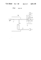
- FIG. 7 is a circuit diagram including a protection circuit according to an embodiment of the present invention.
- an inverter circuit 10 having MIS transistors 10a and 10b as an internal circuit 9 is connected with an input bonding electrode 1, a GND bonding electrode 2 and a V DD bonding electrode 3 respectively, and an output voltage V O is extracted from a junction between the MIS transistors 10a and 10b.
- a protection circuit 8b is provided between gates of the MIS transistors 10a and 10b and the input bonding electrode 1.
- the protection circuit 8b is formed by a protective resistor 4 and a resistor 6 which are connected in series between the input bonding electrode 1 and the internal circuit 9, a first NPN bipolar transistor 7a having a emitter connected between the protective resistor 4 and the collector 6 and an emitter and a base connected to the GND bonding electrode 2 and a second NPN bipolar transistor 7b having an emitter connected beween the protective resistor 4 and the resistor 6, a collector connected to the V DD bonding electrode 3 and a base connected to the GND bonding electrode 2 through resistor 5a.
- Parasitic resistances 5a and 5b are generated by interconnection between the first bipolar transistor 7a and the GND bonding electrode 2 and between the second bipolar transistor 7b and the V DD bonding electrode 3 respectively.
- FIG. 8 is a schematic plan pattern diagram of the bipolar transistors 7a and 7b as shown in FIG. 7, and FIG. 9 is a sectional view taken along the line IX--IX in FIG. 8, typically illustrating wiring etc.
- a P-type semiconductor substrate 17 is provided on its major surface with an N + -type active layer 14a and a field oxide film 16, N + -type active layer 14c and 14d, a field oxide film 16, a P + -type active layer 15 and a field oxide film 16 enclosing the same.
- the innermost field oxide film 16 is connected with the second field oxide film 16, to insulate/separate the N + -type active layers 14c and 14d from each other.
- An input wire 11 is connected with the protective resistor 4 which is connected with the input bonding elecrode 1, the N + -type active layer 14a and the resistor 6 which is connected with the internal circuit 9, through contacts 13 respectively.
- a GND wire 12 is connected to the N + -type active layer 14c and the P + -type active layer 15 through contacts 13, and a V DD wire 21 is connected to the N + -type active layer 14d through contacts 13.
- the N + -type active layers 14a and 14c, the P-type semiconductor substrate 17 and the P + -type active layer 15 form a first NPN bipolar transistor, and the N + -type active layers 14a and 14d, the P-type semiconductor substrate 17 and the P + -type active layer 15 form a second NPN bipolar transistor.
- the current developed in the protective resistor 4 by the high voltage applied to the input bonding electrode 1 is separated into the parasitic resistances 5a and 5b.
- the parasitic resistances 5a and 5b form parallel resistance, the total resistance value of which is smaller than the resistance value of the parasitic resistance 5a or 5b. This means that influence by the parasitic resistance 5a, which has been conventionally disadvantageous with respect to the protective resistor 4, is reduced.
- FIG. 10 is a schematic plan view showing an example in which the embodiment of the present invention is applied to the positional relation between the components as shown in FIG. 6.
- an input bonding electrode 1, a V DD bonding electrode 3 and an internal circuit 9 are connected with each other through a protection circuit 8b in a position separated from a GND bonding electrode 2. Due to such positional relation, a parasitic resistance 5a of a wire connected to the GND bonding electrode 2 from the protection circuit 8b is larger in resistance value than a parasitic resistance 5b of a wire connected to the V DD bonding electrode 3 from the protection circuit 8b. In general, the V DD bonding electrode 3 is thus separated from the GND bonding electrode 2 on an integrated circuit. In this case, therefore, current developed by high voltage applied to the input bonding electrode 1 flows to the V DD bonding electrode 3 mainly through the parasitic resistance 5b. Thus, influence by the parasitic resistance 5a, which has been particularly problematic by such arrangement in the conventional case, is extremely reduced, so that the present invention can contribute to improvement in electrostatic destruction resistance of the internal circuit 9.
- the gate of the second bipolar transistor is connected to the GND bonding electrode in the above embodiment, the same may be connected to the V DD bonding electrode.
- first and second bipolar transistors are of NPN type in the above embodiment, the same may be of PNP type with respective electrodes thereof being appropriately changed in connection.
Landscapes
- Semiconductor Integrated Circuits (AREA)
- Metal-Oxide And Bipolar Metal-Oxide Semiconductor Integrated Circuits (AREA)
- Bipolar Integrated Circuits (AREA)
- Bipolar Transistors (AREA)
Applications Claiming Priority (2)
| Application Number | Priority Date | Filing Date | Title |
|---|---|---|---|
| JP62003712A JPH0821632B2 (ja) | 1987-01-10 | 1987-01-10 | 半導体集積回路 |
| JP62-3712 | 1987-01-10 |
Publications (1)
| Publication Number | Publication Date |
|---|---|
| US4811155A true US4811155A (en) | 1989-03-07 |
Family
ID=11564939
Family Applications (1)
| Application Number | Title | Priority Date | Filing Date |
|---|---|---|---|
| US07/142,558 Expired - Lifetime US4811155A (en) | 1987-01-10 | 1988-01-11 | Protection circuit for a semiconductor integrated circuit having bipolar transistors |
Country Status (2)
| Country | Link |
|---|---|
| US (1) | US4811155A (ja) |
| JP (1) | JPH0821632B2 (ja) |
Cited By (22)
| Publication number | Priority date | Publication date | Assignee | Title |
|---|---|---|---|---|
| US4891729A (en) * | 1982-06-30 | 1990-01-02 | Fujitsu Limited | Semiconductor integrated-circuit apparatus |
| US4937471A (en) * | 1987-11-30 | 1990-06-26 | Samsung Electronics Co., Ltd. | Bidirectional input-output cell |
| US4996626A (en) * | 1988-10-14 | 1991-02-26 | National Semiconductor Corp. | Resistorless electrostatic discharge protection device for high speed integrated circuits |
| US5010380A (en) * | 1989-05-17 | 1991-04-23 | David Sarnoff Research Center, Inc. | Voltage stress alterable ESD protection structure |
| US5191498A (en) * | 1989-01-27 | 1993-03-02 | Gemplus Card International | Safety decive for integrated circuit |
| US5208475A (en) * | 1991-01-30 | 1993-05-04 | National Semiconductor Corporation | Electrostatic discharge protection device and a method for simultaneously forming MOS devices with both lightly doped and non lightly doped source and drain regions |
| US5246872A (en) * | 1991-01-30 | 1993-09-21 | National Semiconductor Corporation | Electrostatic discharge protection device and a method for simultaneously forming MOS devices with both lightly doped and non lightly doped source and drain regions |
| US5359211A (en) * | 1991-07-18 | 1994-10-25 | Harris Corporation | High voltage protection using SCRs |
| EP0663694A1 (en) * | 1993-12-24 | 1995-07-19 | Nec Corporation | Semiconductor device having a protective circuit against electrostatic discharge |
| EP0730300A1 (en) * | 1995-02-28 | 1996-09-04 | STMicroelectronics S.r.l. | Device for the protection of an integrated circuit against electrostatic discharges |
| EP0735640A1 (en) * | 1995-03-31 | 1996-10-02 | Kabushiki Kaisha Toshiba | Protection circuit for semiconductor devices |
| US5663860A (en) * | 1996-06-28 | 1997-09-02 | Harris Corporation | High voltage protection circuits |
| US5663678A (en) * | 1996-02-02 | 1997-09-02 | Vanguard International Semiconductor Corporation | ESD protection device |
| US5745323A (en) * | 1995-06-30 | 1998-04-28 | Analog Devices, Inc. | Electrostatic discharge protection circuit for protecting CMOS transistors on integrated circuit processes |
| US5751525A (en) * | 1996-01-05 | 1998-05-12 | Analog Devices, Inc. | EOS/ESD Protection circuit for an integrated circuit with operating/test voltages exceeding power supply rail voltages |
| US5781389A (en) * | 1994-09-14 | 1998-07-14 | Oki Electric Industry Co., Ltd. | Transistor protection circuit |
| US5789785A (en) * | 1995-02-28 | 1998-08-04 | Sgs-Thomson Microelectronics S.R.L. | Device for the protection of an integrated circuit against electrostatic discharges |
| US5838146A (en) * | 1996-11-12 | 1998-11-17 | Analog Devices, Inc. | Method and apparatus for providing ESD/EOS protection for IC power supply pins |
| US5917689A (en) * | 1996-09-12 | 1999-06-29 | Analog Devices, Inc. | General purpose EOS/ESD protection circuit for bipolar-CMOS and CMOS integrated circuits |
| US6456474B2 (en) * | 1998-04-07 | 2002-09-24 | Nec Corporation | Semiconductor integrated circuit |
| US6587320B1 (en) | 2000-01-04 | 2003-07-01 | Sarnoff Corporation | Apparatus for current ballasting ESD sensitive devices |
| US20100230719A1 (en) * | 2009-03-11 | 2010-09-16 | Nec Electronics Corporation | Esd protection element |
Families Citing this family (4)
| Publication number | Priority date | Publication date | Assignee | Title |
|---|---|---|---|---|
| JPH02119262A (ja) * | 1988-10-28 | 1990-05-07 | Toshiba Corp | 半導体装置 |
| JP2644342B2 (ja) * | 1989-09-01 | 1997-08-25 | 東芝マイクロエレクトロニクス株式会社 | 入力保護回路を備えた半導体装置 |
| JP2753191B2 (ja) * | 1992-10-05 | 1998-05-18 | 松下電器産業株式会社 | 半導体装置 |
| JPH07122715A (ja) * | 1994-04-27 | 1995-05-12 | Toshiba Corp | 半導体装置 |
Citations (4)
| Publication number | Priority date | Publication date | Assignee | Title |
|---|---|---|---|---|
| US4476476A (en) * | 1979-04-05 | 1984-10-09 | National Semiconductor Corporation | CMOS Input and output protection circuit |
| JPS59198762A (ja) * | 1983-04-25 | 1984-11-10 | Seiko Epson Corp | 保護回路 |
| US4617482A (en) * | 1983-10-12 | 1986-10-14 | Nec Corporation | Complementary type MOS field-effect transistor circuit provided with a gate protection structure of small time constant |
| JPH0685551A (ja) * | 1992-09-04 | 1994-03-25 | Hitachi Ltd | 広帯域増幅回路 |
Family Cites Families (1)
| Publication number | Priority date | Publication date | Assignee | Title |
|---|---|---|---|---|
| JPS61218143A (ja) * | 1985-03-25 | 1986-09-27 | Hitachi Ltd | 半導体集積回路装置 |
-
1987
- 1987-01-10 JP JP62003712A patent/JPH0821632B2/ja not_active Expired - Lifetime
-
1988
- 1988-01-11 US US07/142,558 patent/US4811155A/en not_active Expired - Lifetime
Patent Citations (4)
| Publication number | Priority date | Publication date | Assignee | Title |
|---|---|---|---|---|
| US4476476A (en) * | 1979-04-05 | 1984-10-09 | National Semiconductor Corporation | CMOS Input and output protection circuit |
| JPS59198762A (ja) * | 1983-04-25 | 1984-11-10 | Seiko Epson Corp | 保護回路 |
| US4617482A (en) * | 1983-10-12 | 1986-10-14 | Nec Corporation | Complementary type MOS field-effect transistor circuit provided with a gate protection structure of small time constant |
| JPH0685551A (ja) * | 1992-09-04 | 1994-03-25 | Hitachi Ltd | 広帯域増幅回路 |
Cited By (26)
| Publication number | Priority date | Publication date | Assignee | Title |
|---|---|---|---|---|
| US4891729A (en) * | 1982-06-30 | 1990-01-02 | Fujitsu Limited | Semiconductor integrated-circuit apparatus |
| US4937471A (en) * | 1987-11-30 | 1990-06-26 | Samsung Electronics Co., Ltd. | Bidirectional input-output cell |
| US4996626A (en) * | 1988-10-14 | 1991-02-26 | National Semiconductor Corp. | Resistorless electrostatic discharge protection device for high speed integrated circuits |
| US5191498A (en) * | 1989-01-27 | 1993-03-02 | Gemplus Card International | Safety decive for integrated circuit |
| US5010380A (en) * | 1989-05-17 | 1991-04-23 | David Sarnoff Research Center, Inc. | Voltage stress alterable ESD protection structure |
| US5246872A (en) * | 1991-01-30 | 1993-09-21 | National Semiconductor Corporation | Electrostatic discharge protection device and a method for simultaneously forming MOS devices with both lightly doped and non lightly doped source and drain regions |
| US5208475A (en) * | 1991-01-30 | 1993-05-04 | National Semiconductor Corporation | Electrostatic discharge protection device and a method for simultaneously forming MOS devices with both lightly doped and non lightly doped source and drain regions |
| US5359211A (en) * | 1991-07-18 | 1994-10-25 | Harris Corporation | High voltage protection using SCRs |
| EP0663694A1 (en) * | 1993-12-24 | 1995-07-19 | Nec Corporation | Semiconductor device having a protective circuit against electrostatic discharge |
| US5521415A (en) * | 1993-12-24 | 1996-05-28 | Nec Corporation | Semiconductor device having a circuit for protecting the device from electrostatic discharge |
| US5781389A (en) * | 1994-09-14 | 1998-07-14 | Oki Electric Industry Co., Ltd. | Transistor protection circuit |
| EP0730300A1 (en) * | 1995-02-28 | 1996-09-04 | STMicroelectronics S.r.l. | Device for the protection of an integrated circuit against electrostatic discharges |
| US5789785A (en) * | 1995-02-28 | 1998-08-04 | Sgs-Thomson Microelectronics S.R.L. | Device for the protection of an integrated circuit against electrostatic discharges |
| US5821797A (en) * | 1995-03-31 | 1998-10-13 | Kabushiki Kaisha Toshiba | Protection circuit for semiconductor devices |
| EP0735640A1 (en) * | 1995-03-31 | 1996-10-02 | Kabushiki Kaisha Toshiba | Protection circuit for semiconductor devices |
| US5745323A (en) * | 1995-06-30 | 1998-04-28 | Analog Devices, Inc. | Electrostatic discharge protection circuit for protecting CMOS transistors on integrated circuit processes |
| US5751525A (en) * | 1996-01-05 | 1998-05-12 | Analog Devices, Inc. | EOS/ESD Protection circuit for an integrated circuit with operating/test voltages exceeding power supply rail voltages |
| US5663678A (en) * | 1996-02-02 | 1997-09-02 | Vanguard International Semiconductor Corporation | ESD protection device |
| US5663860A (en) * | 1996-06-28 | 1997-09-02 | Harris Corporation | High voltage protection circuits |
| US5917689A (en) * | 1996-09-12 | 1999-06-29 | Analog Devices, Inc. | General purpose EOS/ESD protection circuit for bipolar-CMOS and CMOS integrated circuits |
| US5838146A (en) * | 1996-11-12 | 1998-11-17 | Analog Devices, Inc. | Method and apparatus for providing ESD/EOS protection for IC power supply pins |
| US6456474B2 (en) * | 1998-04-07 | 2002-09-24 | Nec Corporation | Semiconductor integrated circuit |
| US6587320B1 (en) | 2000-01-04 | 2003-07-01 | Sarnoff Corporation | Apparatus for current ballasting ESD sensitive devices |
| US20100230719A1 (en) * | 2009-03-11 | 2010-09-16 | Nec Electronics Corporation | Esd protection element |
| US8860139B2 (en) | 2009-03-11 | 2014-10-14 | Renesas Electronics Corporation | ESD protection element |
| US9177949B2 (en) | 2009-03-11 | 2015-11-03 | Renesas Electronics Corporation | ESD protection element |
Also Published As
| Publication number | Publication date |
|---|---|
| JPS63172454A (ja) | 1988-07-16 |
| JPH0821632B2 (ja) | 1996-03-04 |
Similar Documents
| Publication | Publication Date | Title |
|---|---|---|
| US4811155A (en) | Protection circuit for a semiconductor integrated circuit having bipolar transistors | |
| JP2850801B2 (ja) | 半導体素子 | |
| US4996626A (en) | Resistorless electrostatic discharge protection device for high speed integrated circuits | |
| US4876584A (en) | Electrostatic discharge protection circuit | |
| US5060037A (en) | Output buffer with enhanced electrostatic discharge protection | |
| JP2731119B2 (ja) | 半導体パワー素子およびその遮断回路 | |
| US4994904A (en) | MOSFET having drain voltage detection function | |
| JPH0558583B2 (ja) | ||
| US4543593A (en) | Semiconductor protective device | |
| JPH0334659B2 (ja) | ||
| JPH03272180A (ja) | 半導体集積回路 | |
| US5811845A (en) | Semiconductor apparatus and horizontal register for solid-state image pickup apparatus with protection circuit for bypassing an excess signal | |
| EP0371663B1 (en) | Integrated circuit output buffer having improved ESD protection | |
| GB2176053A (en) | Device for protection against electrostatic discharges for bipolar integrated circuits | |
| US5828107A (en) | Semiconductor integrated circuit device | |
| JPH05505060A (ja) | 低トリガ電圧scr保護装置及び構造 | |
| JP3390040B2 (ja) | 集積回路 | |
| EP0198468A2 (en) | Protective device for integrated circuit | |
| JP2580571B2 (ja) | 入力保護回路 | |
| JPH0715010A (ja) | 半導体装置の保護回路 | |
| JPS6211787B2 (ja) | ||
| JPS58186959A (ja) | 半導体装置 | |
| JPH06151716A (ja) | 半導体集積回路装置 | |
| JPS58202573A (ja) | 半導体集積回路装置 | |
| US5432369A (en) | Input/output protection circuit |
Legal Events
| Date | Code | Title | Description |
|---|---|---|---|
| AS | Assignment |
Owner name: MITSUBISHI DENKI KABUSHIKI KAISHA, 2-3 MARUNOUCHI Free format text: ASSIGNMENT OF ASSIGNORS INTEREST.;ASSIGNORS:KURIYAMA, HIROTADA;WADA, TOMOHISA;MURAKAMI, SHUUJI;REEL/FRAME:004821/0150;SIGNING DATES FROM |
|
| STCF | Information on status: patent grant |
Free format text: PATENTED CASE |
|
| FEPP | Fee payment procedure |
Free format text: PAYOR NUMBER ASSIGNED (ORIGINAL EVENT CODE: ASPN); ENTITY STATUS OF PATENT OWNER: LARGE ENTITY |
|
| FPAY | Fee payment |
Year of fee payment: 4 |
|
| FPAY | Fee payment |
Year of fee payment: 8 |
|
| FPAY | Fee payment |
Year of fee payment: 12 |