US4821166A - Power-supply circuit - Google Patents
Power-supply circuit Download PDFInfo
- Publication number
- US4821166A US4821166A US07/164,315 US16431588A US4821166A US 4821166 A US4821166 A US 4821166A US 16431588 A US16431588 A US 16431588A US 4821166 A US4821166 A US 4821166A
- Authority
- US
- United States
- Prior art keywords
- power
- storage means
- supply circuit
- voltage source
- voltage
- Prior art date
- Legal status (The legal status is an assumption and is not a legal conclusion. Google has not performed a legal analysis and makes no representation as to the accuracy of the status listed.)
- Expired - Fee Related
Links
- 239000003990 capacitor Substances 0.000 claims description 25
- 238000009966 trimming Methods 0.000 claims description 6
- 230000002401 inhibitory effect Effects 0.000 claims description 5
- 230000008859 change Effects 0.000 claims description 2
- 238000005259 measurement Methods 0.000 description 6
- 238000010586 diagram Methods 0.000 description 5
- 230000001965 increasing effect Effects 0.000 description 4
- 230000003071 parasitic effect Effects 0.000 description 4
- 101150109657 ureF gene Proteins 0.000 description 4
- 230000007423 decrease Effects 0.000 description 3
- 230000000737 periodic effect Effects 0.000 description 2
- 230000002441 reversible effect Effects 0.000 description 2
- 230000001629 suppression Effects 0.000 description 2
- 238000012546 transfer Methods 0.000 description 2
- 238000004804 winding Methods 0.000 description 2
- 230000008901 benefit Effects 0.000 description 1
- 238000004891 communication Methods 0.000 description 1
- 238000010276 construction Methods 0.000 description 1
- 230000001419 dependent effect Effects 0.000 description 1
- 238000004146 energy storage Methods 0.000 description 1
- 230000002349 favourable effect Effects 0.000 description 1
- 230000001939 inductive effect Effects 0.000 description 1
- 238000002955 isolation Methods 0.000 description 1
- 238000012986 modification Methods 0.000 description 1
- 230000004048 modification Effects 0.000 description 1
- 238000012545 processing Methods 0.000 description 1
- 230000009467 reduction Effects 0.000 description 1
- 230000000630 rising effect Effects 0.000 description 1
Images


Classifications
-
- H—ELECTRICITY
- H02—GENERATION; CONVERSION OR DISTRIBUTION OF ELECTRIC POWER
- H02M—APPARATUS FOR CONVERSION BETWEEN AC AND AC, BETWEEN AC AND DC, OR BETWEEN DC AND DC, AND FOR USE WITH MAINS OR SIMILAR POWER SUPPLY SYSTEMS; CONVERSION OF DC OR AC INPUT POWER INTO SURGE OUTPUT POWER; CONTROL OR REGULATION THEREOF
- H02M3/00—Conversion of DC power input into DC power output
- H02M3/02—Conversion of DC power input into DC power output without intermediate conversion into AC
- H02M3/04—Conversion of DC power input into DC power output without intermediate conversion into AC by static converters
- H02M3/10—Conversion of DC power input into DC power output without intermediate conversion into AC by static converters using discharge tubes with control electrode or semiconductor devices with control electrode
- H02M3/145—Conversion of DC power input into DC power output without intermediate conversion into AC by static converters using discharge tubes with control electrode or semiconductor devices with control electrode using devices of a triode or transistor type requiring continuous application of a control signal
- H02M3/155—Conversion of DC power input into DC power output without intermediate conversion into AC by static converters using discharge tubes with control electrode or semiconductor devices with control electrode using devices of a triode or transistor type requiring continuous application of a control signal using semiconductor devices only
- H02M3/156—Conversion of DC power input into DC power output without intermediate conversion into AC by static converters using discharge tubes with control electrode or semiconductor devices with control electrode using devices of a triode or transistor type requiring continuous application of a control signal using semiconductor devices only with automatic control of output voltage or current, e.g. switching regulators
-
- H—ELECTRICITY
- H02—GENERATION; CONVERSION OR DISTRIBUTION OF ELECTRIC POWER
- H02M—APPARATUS FOR CONVERSION BETWEEN AC AND AC, BETWEEN AC AND DC, OR BETWEEN DC AND DC, AND FOR USE WITH MAINS OR SIMILAR POWER SUPPLY SYSTEMS; CONVERSION OF DC OR AC INPUT POWER INTO SURGE OUTPUT POWER; CONTROL OR REGULATION THEREOF
- H02M1/00—Details of apparatus for conversion
- H02M1/12—Arrangements for reducing harmonics from AC input or output
Definitions
- This invention relates to a power-supply circuit
- a power-storage means for storing the power supplied by an a.c. source in specific time intervals in which the alternating voltage source is connected to said power-storage means, comprising a switch for taking power from the power storage means, and comprising a control circuit for periodically actuating the switch.
- the switching operations of the periodically actuated switching transistor give rise to undesired high-frequency voltages and currents on the a.c. source, i.e. for example on the a.c. mains, which may give rise to interference in, for example, further loads powered by the alternating voltage source.
- passive high-frequency filters comprising coils, capacitors and, if required, resistors between the a.c. source and the other sections of the other circuit arrangement.
- Such an interference filter is mentioned in "Schaltnetzmaschine in der Kir" in the caption to FIG. 5.1 on page 105.
- Such filters are complex and expensive, and they also occupy a substantial part of the total circuit volume.
- control circuit is adapted to actuate the switch only at times that fall outside the time interval in which the alternating voltage source is connected to the power storage means.
- the invention is based on the recognition of the fact that the interference caused by the periodic actuation of the switch is transferred to the a.c. source only if said source is connected to the power-storage means for the purpose of supplying power to said means. According to the invention the actuation of the switch is inhibited in these time intervals, so that no interference is produced in these intervals. For the remainder of the time, in which the a.c. source is isolated from the power-storage means, the interference produced by the switch is kept at least substantially away from the a.c. source as a result of said isolation. This makes it possible to dispense with an interference filter of a conventional type.
- the a.c. source and the power-storage means are connected and disconnected from one another by a rectifier stage for feeding power from the a.c. source into the power-storage means.
- a rectifier stage for feeding power from the a.c. source into the power-storage means.
- the actuation of the switch is inhibited, so that no interference can be transferred from this switch to the a.c. source via the conductive rectifier stage.
- the a.c. source is a power-supply mains.
- the invention then precludes the inrush of interference into said mains and thus prevents the interference from reaching other loads powered by said mains, such as for example electronic equipment for communication or data processing.
- the a.c. source may alternatively be a chopper circuit or the like, which is then protected against interference from subsequent circuitry by means of the invention.
- the recitifer stage may also be advantageous to shunt the recitifer stage with a capacitive arrangement.
- Such an arrangement enables interference across the rectifier stage to be short-circuited so that it cannot be transferred to the a.c. source and, moreover, it enables asymmetries in the reverse impedances of the rectifier stage to be compensated for and to preclude the parasitic transfer of interference caused by said asymmetries.
- FIG. 1 shows a prior-art circuit arrangement
- FIGS. 2 and 3 give voltage and current waveforms in the circuit arrangement of FIG. 1,
- FIGS. 4 and 6 show three embodiments of the invention
- FIG. 7 gives signal waveforms in the circuit arrangement of FIG. 6,
- FIGS. 8 and 9 show examples of modifications of the invention.
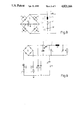
- FIG. 1 shows a prior-art circuit arrangement for supplying power from an a.c. source 1 to a load 8 via a powerstorage means 6.
- the a.c. source 1 is a power-supply mains whose line resistance is represented by two mains impedances 2, 3 in the equivalent diagram of FIG. 1.
- the alternating mains voltage UW is applied from the a.c. source 1 to a rectifier stage via a high-frequency filter 4, which functions as an interference filter.
- the rectifier stage comprises a four-diode bridge rectifier 5.
- the rectified alternating mains voltage charges the power-storage means 6.
- Said means suitably comprise an electrolytic capacitor whose H.F. equivalent diagram is shown in FIG. 1.
- the power-storage means 6 may comprise a storage batttery, which in the HF equivalent diagram of FIG. 1 takes the place of the capacitor 60.
- the power-storage means 6 is connected to a switchedmode power supply 7 via which the load 8 is powered from the power-storage means 6.
- the power supply 7 comprises a transistor 10, which serves as a periodically actuated switch, and a coil 9 arranged in series with the load 8.
- the series arrangement comprising the load 8, the coil 9 and the transistor 10 is connected in parallel with the power-storage means 6.
- the series arrangement comprising the coil 9 and the load 8 is shunted by a freewheel diode 11, and a capacitor 12 is arranged in parallel with the load 8.
- FIG. 2 shows current and voltage waveforms relating to the supply of power from the a.c. source 1 into the powerstorage means 6 for the time interval TW corresponding to one half-cycle of the alternating mains voltage UW.
- the time t is plotted on the horizontal axis.
- the broken line indicates the variation of the voltage UC across the powerstorage means 6.
- the voltage UC is higher than the alternating mains voltage UW. Consequently, the bridge rectifier 5 is cut off and no current flows from the alternating voltage source 1 into the power-storage means 6.
- the voltage UC decreases in conformity with the power consumed by the load 8.
- the bridge rectifier 5 becomes conductive and a charging current IC is produced in the power-storage means 6. Its waveform is shown in FIG. 2.
- the voltage UC across the power-storage means 6 now follows the variation of the alternating mains voltage UW until this voltage has reached its peak value and decreases at a rate higher than that of the voltage UC which is dictated by the power taken by the switched-mode power supply 7. From this instant t2 the alternating mains voltage UW is again smaller than the voltage UC across the power-storage means 6 and the charging current IC becomes 0. Consequently, what has been stated for the time interval from 0 to t1 also applies to the time interval from t2 to TW.
- FIG. 3 shows two current waveforms.
- the transistor 10 is periodically turned on and off at a switching frequency which is high compared to the frequency of the alternating voltage UW. If the frequency of the alternating mains voltage UW is, for example, 50 Hz the transistor 10 is generally switched at a frequency of at least 20 kHz.
- Both the powerstorage means 6 and the capacitor 12 are dimensioned in such a way, relative to the actuation period TS of the transistor 10, that the voltages across them do not noticeably follow the sawtooth-shaped currents IT and IL, so that the load 8 is always powered with a smoothed direct voltage.
- the currents IT and IL then act on substantially constant voltages and therefore exhibit at least substantially linear edges.
- the current IT through the transistor 10 via the junction point a is furnished only partly by the power-storage means 6 and for the remainder it is supplied directly by the a.c. source 1 via the rectifier bridge 5.
- This division depends on the impedance of the rectifier bridge 5, the mains impedances 2, 3 and the impedances of the power-storage means 6, i.e. in particular the line resistance 61 and the line inductance 62.
- the fraction of the current IT derived from the a.c. source 1 via the rectifier bridge 5 forms the interference to be suppressed by means of the invention.
- the power-storage means 6 for example an electrolytic capacitor, will behave as a series tuned circuit whose impedance above the resonant frequency is dictated by the line inductance 62.
- This inductive reactance increases with the frequency so that an increasing fraction of the transistor current IT is supplied directly by the a.c. source 1 via the rectifier bridge 5.
- the amount of interference transmitted to the a.c. source 1 largely depends on the state of the rectifier bridge 5.
- the rectifier bridge In the time interval between t1 and t2 the rectifier bridge is conductive and together with the low mains impedances 2 and 3 it constitutes a low resistance via which a substantial portion of the transistor current IT flows.
- the mains impedances are smaller than or equal to 50 ohms at the frequency of the current IT.
- the rectifier bridge 5 In the other time intervals of the half-cycle of the alternating mains voltage UW the rectifier bridge 5 is cut off and thus constitutes a very high resistance, which in principle is dictated by the reverse capacitance of the rectifier bridge 5, for example, by the bridge diodes with their depletion-layer capacitances. These depletion-layer capacitances are of the order of magnitude of a few picofarads and constitute such a high resistance that substantially the entire transistor current IT is supplied by the power-storage means 6.
- the invention utilizes the different behaviour of the circuit arrangement as described above and prevents interference from reaching the a.c. source 1 in that in the time intervals in which the rectifier bridge 5 is conductive the drive to the transistor 10 is interrupted and hence no interference can be produced.
- the high-frequency filter 4 may then be dispensed with. In the circuit arrangement shown in FIG. 1 this filter is replaced by a device for inhibiting the periodic drive of the transistor 10.
- FIG. 4 An example of such a circuit arrangement is shown in FIG. 4, in which the parts of the circuit described above bear the same reference numerals.
- the control circuit 13 In the switched-mode power supply 7 the control circuit 13 is also shown. This control circuit periodically turns on the transistor 10 and for this purpose it is connected to the base of this transistor via a line 30.
- a measurement resistor 31 of low resistance is arranged in the connection between the rectifier bridge 5 and the junction point A and across this resistor a small voltage drop is produced when the charging current IC flows in the time interval t1 to t2.
- the resistance value of the measurement resistor 31 is dimensioned in such a way that the voltage drop produced by the charging current IC can be detected reliably by a following measurement amplifier 32, but produces only a minimal loss of power.
- the measurement amplifier 32 On its output 33 the measurement amplifier 32 produces a digital inhibit signal, which assumes the logic value 0 when the charging current IC flows and which has the logic value 1 in the other time intervals. As a result of this, an AND circuit 34 arranged in the line to the transistor 10 is opened and the transistor 10 is turned off in the time interval between t1 and t2.
- FIG. 5 shows such a circuit arrangement in which the elements already described bear the same reference numerals.
- a series arrangement comprising two oppositely poled diodes 14, 15 is connected to the a.c. source 1, in parallel with the rectifier bridge 5, so that the rectified non-smoothed alternating mains voltage, i.e. a waveform as represented by UW in FIG. 2, appears at the junction point 35 between said diodes.
- the measurement amplifier 32 this voltage is compared with the voltage UC across the power-storage means 6.
- the inhibit signal appearing on its output 33 assumes the same values as described for the circuit arrangement of FIG. 4.
- FIG. 6 shows a third embodiment comprising a timegate circuit.
- This circuit comprises a comparator 18 and two monostable multivibrators 19 and 20. Identical parts bear the same reference numerals as in the arrangements described above.
- the rectified non-smoothed alternating mains voltage UW is applied from the junction point 35 between the diodes 14, 15 to a first input 36 of the comparator 18 via a voltage divider comprising two resistors 16, 17, a reference voltage UREF is applied to the second input 37.
- the comparator 18 comprises a differential amplifier whose inverting input is the first input 36 and whose non-inverting input is the second input 37 of the comparator 18.
- FIG. 7 shows some signal waveforms relating to the arrangement of FIG. 6.
- FIG. 7a shows the voltage UWK obtained on the first input 36 of the comparator 18 after rectification by means of the diodes 14 and 15 and subsequent division in the voltage divider 16, 17.
- the reference voltage UREF is represented as a broken line. This reference voltage is low relative to the amplitude of the voltage UWK, so that, for the greater part of the period TW of one half-cyle of the alternating main voltage, UWK is higher than the reference voltage UREF.
- the voltage UWK becomes smaller than the value of the voltage UREF only in the direct proximity of the zero crossings of the alternating mains voltage UW, i.e. for example near the instant 0 and the instant TW. In these small time intervals the voltage U38 on the output 38 of the comparator 18 assumes a high value, whereas it is zero in the other time intervals.
- FIG. 7b shows the voltage U38 as a function of time.
- the voltage U38 on the output 38 of the comparator 18 is applied to an input of the first monostable multivibrator 19.
- This multivibrator further comprises an output 39, on which a voltage U39 appears, whose variation is shown in FIG. 7c.
- Each rising edge of the voltage U38 produces a positive voltage pulse on the output 39 of the first monostable 19, which pulse terminates a time interval t1 after the beginning of the half-cycle of the alternating mains voltage UW during which the pulse in the voltage U38 is produced.
- the pulses of the voltage U39 are applied to an input of the second monostable multivibrator 20, which input is connected to the output 39 of the first monostable 19.
- the falling edges of the voltage U39 produce negative voltage pulses of a length t2-t1 on the output 40 of the second monostable 20. These pulses are shown as the waveform U40 in FIG. 7d. They define a time gate which corresponds exactly to the time interval in which the charging current IC flows.
- the voltage U40 is applied to the AND-circuit 34 via the output 40 and during said time gate it inhibits the drive of the transistor 10 via the line 30.
- the time gate may be slightly larger than the time interval between t1 and t2.
- FIG. 8 shows an example of a further embodiment of the invention, which enables interference produced across the a.c. source 1 by the transistor 10 to be reduced even further.
- interference across the rectifier bridge 5 caused by the current IT occurs only in those time intervals in which the diodes of the rectifier bridge 5 are cut off.
- the depletion-layer capacitances of the diodes are then operative. They constitute a bridge arrangement in whose diagonal arm the series arrangement of the voltage source 1 and the mains impedances 2, 3 is situated. If the values of the depletion-layer capacitances of all the diodes are identical, the bridge is balanced and no interference can reach the a.c. source 1.
- the depletion-layer capacitances of the diodes depend strongly on the voltages across these diodes. However, these voltages change constantly as a result of the alternating mains voltage UW, so that even in the case of identical diodes balancing is achieved only during the zero crossings of the alternating mains voltage UW.
- the diodes of the rectifier bridge 5 are therefore shunted by a capacitive arrangement comprising four trimming capacitors 41, 42, 43, 44 which are each arranged in parallel with interference ones of the diodes of the rectifier bridge 5.
- the trimming capacitors 41, 42, 43, 44 have large capacitances in comparison with the maximum depletion-layer capacitances of the diodes that can be reached by driving said diodes with the alternating mains voltage UW. In fact, the balance of the rectifier bridge 5 depends on the trimming capacitors 41, 42, 43, 44 and is then largely independent of the alternating mains voltage UW applied to the rectifier bridge 5. In this way the transfer of interference to the a.c. source by the current IT is reduced even further.
- the invention also reduces asymmetrical interference.
- Such interference occurs, for example, if the potential after the transistor 10, i.e. at the junction point B between the transistor 10, the coil 9 and the freewheel diode 11, is switched between a low value near ground potential and a high value near the voltage UC as a result of the transistor 10 and the freewheel diode 11 being turned on and turned off alternately. Since parasitic capacitances between the junction point B and the ground lines cannot be avoided completely, capacitive currents will flow which are in phase and which are in principle distributed equally between the two mains impedances 2, 3 in FIG. 1.
- the shunt capacitors 22, 23 are arranged in parallel with the arrangement comprising the a.c. source 1, the mains impedances 2, 3 and the rectifier bridge 5, said capacitors being dimensioned in such a way that for the current IS they present a substantially lower impedance than the cut-off rectifier bridge 5. This enables such interference components to be suppressed very effectively with simple means, i.e. with capacitors of comparatively low capacitance values.
- the invention enables a very simple and compact construction to be obtained, even if both the shunt capacitors 22, 23 in FIG. 9 and the trimming capacitors 41, 42, 43 44 in FIG. 8 are used.
- the advantage of a simplified arrangement is also maintained if, in accordance with the invention, the power supply to the load 8 is inhibited during the time intervals in which the charging current IC flows and the capacitor 12 must therefore be dimensioned accordingly. It is particularly favourable if the capacitor 12 is replaced by a storage battery arranged in parallel with the load, which enables the charging intervals to be chosen more freely.
Landscapes
- Engineering & Computer Science (AREA)
- Power Engineering (AREA)
- Rectifiers (AREA)
- Transmitters (AREA)
- Dc-Dc Converters (AREA)
- Power Conversion In General (AREA)
- Arrangements For Transmission Of Measured Signals (AREA)
- Electrotherapy Devices (AREA)
- Apparatus For Radiation Diagnosis (AREA)
- Air Bags (AREA)
- Input Circuits Of Receivers And Coupling Of Receivers And Audio Equipment (AREA)
- Stand-By Power Supply Arrangements (AREA)
Applications Claiming Priority (2)
| Application Number | Priority Date | Filing Date | Title |
|---|---|---|---|
| DE19873722337 DE3722337A1 (de) | 1987-07-07 | 1987-07-07 | Schaltungsanordnung zum uebertragen elektrischer energie |
| DE3722337 | 1987-07-07 |
Publications (1)
| Publication Number | Publication Date |
|---|---|
| US4821166A true US4821166A (en) | 1989-04-11 |
Family
ID=6331025
Family Applications (1)
| Application Number | Title | Priority Date | Filing Date |
|---|---|---|---|
| US07/164,315 Expired - Fee Related US4821166A (en) | 1987-07-07 | 1988-03-04 | Power-supply circuit |
Country Status (6)
| Country | Link |
|---|---|
| US (1) | US4821166A (fr) |
| EP (1) | EP0298562B1 (fr) |
| JP (1) | JP2697862B2 (fr) |
| AT (1) | ATE95351T1 (fr) |
| BR (1) | BR8803318A (fr) |
| DE (2) | DE3722337A1 (fr) |
Cited By (28)
| Publication number | Priority date | Publication date | Assignee | Title |
|---|---|---|---|---|
| US4992921A (en) * | 1988-11-30 | 1991-02-12 | U.S. Philips Corporation | Circuit arrangement for supplying a load |
| US5128854A (en) * | 1988-11-30 | 1992-07-07 | U.S. Philips Corporation | Circuit arrangement for supplying a load |
| US5267137A (en) * | 1990-10-19 | 1993-11-30 | Kohler, Schmid Partner | High-power power supply |
| US5339019A (en) * | 1990-12-24 | 1994-08-16 | Alcatel N.V. | Current sink |
| US5341285A (en) * | 1992-07-14 | 1994-08-23 | Wave Energy Corporation | Intelligent transformerless system for transferring energy from a power source to an isolated load |
| US5416687A (en) * | 1992-06-23 | 1995-05-16 | Delta Coventry Corporation | Power factor correction circuit for AC to DC power supply |
| US5500561A (en) * | 1991-01-08 | 1996-03-19 | Wilhelm; William G. | Customer side power management system and method |
| US5513092A (en) * | 1993-07-19 | 1996-04-30 | Bruker Analytische Messtechnik Gmbh | Precision regulated low loss high-power power supply |
| US5561596A (en) * | 1994-02-22 | 1996-10-01 | International Business Machines Corporation | AC line stabilization circuitry for high power factor loads |
| US5587894A (en) * | 1994-03-28 | 1996-12-24 | Matsushita Electric Works, Ltd. | Power source device |
| US5604426A (en) * | 1993-06-30 | 1997-02-18 | Asahi Glass Company Ltd. | Electric apparatus with a power supply including an electric double layer capacitor |
| US5612856A (en) * | 1993-11-19 | 1997-03-18 | U.S. Philips Corporation | Circuit arrangement for producing a direct voltage with reduction of harmonic and high-frequency interferences |
| US5701240A (en) * | 1996-03-05 | 1997-12-23 | Echelon Corporation | Apparatus for powering a transmitter from a switched leg |
| US5703766A (en) * | 1996-03-05 | 1997-12-30 | Echelon Corporation | Capacitor power supply for intermittent transmission |
| US5786642A (en) * | 1991-01-08 | 1998-07-28 | Nextek Power Systems Inc. | Modular power management system and method |
| US5877614A (en) * | 1996-12-18 | 1999-03-02 | Siemens Aktiengesellschaft | Electronic switch-mode power supply |
| US5969435A (en) * | 1991-01-08 | 1999-10-19 | Nextek Power Systems, Inc. | Modular DC cogenerator systems |
| US6043635A (en) * | 1996-05-17 | 2000-03-28 | Echelon Corporation | Switched leg power supply |
| US6157179A (en) * | 1997-06-13 | 2000-12-05 | U.S. Philips Corporation | Switched-mode power supply for charging a capacitance during a first period, forming a resonant circuit with an inductance, and discharging the capacitance into a load during a second period disjunct from the first period |
| US6252310B1 (en) * | 1999-07-28 | 2001-06-26 | Nextek Power Systems, Inc. | Balanced modular power management system and method |
| WO2001078224A1 (fr) * | 2000-04-10 | 2001-10-18 | Fisher & Paykel Appliances Limited | Alimentation electrique pour appareils |
| US6933627B2 (en) | 1991-01-08 | 2005-08-23 | Nextek Power Systems Inc. | High efficiency lighting system |
| US20080238331A1 (en) * | 2007-03-30 | 2008-10-02 | Hon Hai Precision Industry Co., Ltd. | Energy saving power supply circuit |
| US20130010509A1 (en) * | 2011-07-08 | 2013-01-10 | Toshiba Lighting & Technology Corporation | Power supply device |
| WO2019086328A1 (fr) | 2017-10-31 | 2019-05-09 | Signify Holding B.V. | Circuit d'alimentation électrique et procédé d'alimentation électrique |
| EP3500067A1 (fr) | 2017-12-14 | 2019-06-19 | Signify Holding B.V. | Circuit et procédé d'alimentation électrique |
| CN115291073A (zh) * | 2022-08-04 | 2022-11-04 | 中广核工程有限公司 | 续流二极管的性能检测装置 |
| US11619956B2 (en) | 2020-03-13 | 2023-04-04 | Hamilton Sundstrand Corporation | Nonlinear trim head power supply with a wide input range and a high efficiency |
Families Citing this family (3)
| Publication number | Priority date | Publication date | Assignee | Title |
|---|---|---|---|---|
| AT402133B (de) * | 1992-10-14 | 1997-02-25 | Fronius Schweissmasch | Steuereinrichtung für die energieversorgung eines verbraucherkreises eines gleichstromverbrauchers und ein verfahren zum betrieb einer derartigen steuereinrichtung |
| JP2008079380A (ja) * | 2006-09-19 | 2008-04-03 | Murata Mfg Co Ltd | 電源装置および電源システム |
| EP2775596A1 (fr) * | 2013-03-07 | 2014-09-10 | Vestel Elektronik Sanayi ve Ticaret A.S. | Alimentation électrique de mode commuté |
Citations (3)
| Publication number | Priority date | Publication date | Assignee | Title |
|---|---|---|---|---|
| DE2718598A1 (de) * | 1977-04-22 | 1978-10-26 | Licentia Gmbh | Stoerstromreduzierende stromrichterbeschaltung |
| DE3025405A1 (de) * | 1980-07-04 | 1982-01-21 | Siemens Ag | Verfahren zum erzielen einer sinusfoermigen stromaufnahme eines gleichstromverbrauchers mit parallelgeschaltetem ladekondensator |
| US4730243A (en) * | 1985-12-23 | 1988-03-08 | Sundstrand Corporation | EMI reduction circuit |
Family Cites Families (4)
| Publication number | Priority date | Publication date | Assignee | Title |
|---|---|---|---|---|
| DE2333570C3 (de) * | 1973-07-02 | 1978-07-20 | Siemens Ag, 1000 Berlin Und 8000 Muenchen | Schaltungsanordnung zur Speisung eines Gleichstromverbrauchers aus einer Wechselstromquelle über einen ungesteuerten Gleichrichter |
| DE3302093A1 (de) * | 1983-01-22 | 1984-07-26 | Grundig E.M.V. Elektro-Mechanische Versuchsanstalt Max Grundig & Co KG, 8510 Fürth | Schaltungsanordnung zur verminderung des oberwellenanteils im netzstrom bei netzgleichrichtung |
| JPS60190164A (ja) | 1984-03-09 | 1985-09-27 | Matsushita Electric Ind Co Ltd | 電源装置 |
| US4626981A (en) * | 1985-08-02 | 1986-12-02 | Rca Corporation | Dual voltage converter circuit |
-
1987
- 1987-07-07 DE DE19873722337 patent/DE3722337A1/de not_active Withdrawn
-
1988
- 1988-03-04 US US07/164,315 patent/US4821166A/en not_active Expired - Fee Related
- 1988-07-04 BR BR8803318A patent/BR8803318A/pt unknown
- 1988-07-05 AT AT88201406T patent/ATE95351T1/de not_active IP Right Cessation
- 1988-07-05 DE DE88201406T patent/DE3884483D1/de not_active Expired - Fee Related
- 1988-07-05 EP EP88201406A patent/EP0298562B1/fr not_active Expired - Lifetime
- 1988-07-07 JP JP63167886A patent/JP2697862B2/ja not_active Expired - Lifetime
Patent Citations (3)
| Publication number | Priority date | Publication date | Assignee | Title |
|---|---|---|---|---|
| DE2718598A1 (de) * | 1977-04-22 | 1978-10-26 | Licentia Gmbh | Stoerstromreduzierende stromrichterbeschaltung |
| DE3025405A1 (de) * | 1980-07-04 | 1982-01-21 | Siemens Ag | Verfahren zum erzielen einer sinusfoermigen stromaufnahme eines gleichstromverbrauchers mit parallelgeschaltetem ladekondensator |
| US4730243A (en) * | 1985-12-23 | 1988-03-08 | Sundstrand Corporation | EMI reduction circuit |
Non-Patent Citations (2)
| Title |
|---|
| "Schaltnetzteile in der Praxis", Kilgenstein, pp. 105-108. |
| Schaltnetzteile in der Praxis , Kilgenstein, pp. 105 108. * |
Cited By (33)
| Publication number | Priority date | Publication date | Assignee | Title |
|---|---|---|---|---|
| US4992921A (en) * | 1988-11-30 | 1991-02-12 | U.S. Philips Corporation | Circuit arrangement for supplying a load |
| US5128854A (en) * | 1988-11-30 | 1992-07-07 | U.S. Philips Corporation | Circuit arrangement for supplying a load |
| US5267137A (en) * | 1990-10-19 | 1993-11-30 | Kohler, Schmid Partner | High-power power supply |
| US5339019A (en) * | 1990-12-24 | 1994-08-16 | Alcatel N.V. | Current sink |
| US5500561A (en) * | 1991-01-08 | 1996-03-19 | Wilhelm; William G. | Customer side power management system and method |
| US5786642A (en) * | 1991-01-08 | 1998-07-28 | Nextek Power Systems Inc. | Modular power management system and method |
| US6933627B2 (en) | 1991-01-08 | 2005-08-23 | Nextek Power Systems Inc. | High efficiency lighting system |
| US5969435A (en) * | 1991-01-08 | 1999-10-19 | Nextek Power Systems, Inc. | Modular DC cogenerator systems |
| US5416687A (en) * | 1992-06-23 | 1995-05-16 | Delta Coventry Corporation | Power factor correction circuit for AC to DC power supply |
| US5341285A (en) * | 1992-07-14 | 1994-08-23 | Wave Energy Corporation | Intelligent transformerless system for transferring energy from a power source to an isolated load |
| US5604426A (en) * | 1993-06-30 | 1997-02-18 | Asahi Glass Company Ltd. | Electric apparatus with a power supply including an electric double layer capacitor |
| US5513092A (en) * | 1993-07-19 | 1996-04-30 | Bruker Analytische Messtechnik Gmbh | Precision regulated low loss high-power power supply |
| US5612856A (en) * | 1993-11-19 | 1997-03-18 | U.S. Philips Corporation | Circuit arrangement for producing a direct voltage with reduction of harmonic and high-frequency interferences |
| US5561596A (en) * | 1994-02-22 | 1996-10-01 | International Business Machines Corporation | AC line stabilization circuitry for high power factor loads |
| US5563758A (en) * | 1994-02-22 | 1996-10-08 | International Business Machines Corporation | Circuit to permit three phase input power supply to operate when one phase drops out and provide lightening protection |
| CN1041674C (zh) * | 1994-03-28 | 1999-01-13 | 松下电工株式会社 | 电源装置 |
| US5587894A (en) * | 1994-03-28 | 1996-12-24 | Matsushita Electric Works, Ltd. | Power source device |
| US5701240A (en) * | 1996-03-05 | 1997-12-23 | Echelon Corporation | Apparatus for powering a transmitter from a switched leg |
| US5703766A (en) * | 1996-03-05 | 1997-12-30 | Echelon Corporation | Capacitor power supply for intermittent transmission |
| US6043635A (en) * | 1996-05-17 | 2000-03-28 | Echelon Corporation | Switched leg power supply |
| US5877614A (en) * | 1996-12-18 | 1999-03-02 | Siemens Aktiengesellschaft | Electronic switch-mode power supply |
| US6157179A (en) * | 1997-06-13 | 2000-12-05 | U.S. Philips Corporation | Switched-mode power supply for charging a capacitance during a first period, forming a resonant circuit with an inductance, and discharging the capacitance into a load during a second period disjunct from the first period |
| US6252310B1 (en) * | 1999-07-28 | 2001-06-26 | Nextek Power Systems, Inc. | Balanced modular power management system and method |
| WO2001078224A1 (fr) * | 2000-04-10 | 2001-10-18 | Fisher & Paykel Appliances Limited | Alimentation electrique pour appareils |
| AU2001252790B2 (en) * | 2000-04-10 | 2004-03-25 | Fisher & Paykel Appliances Limited | Appliance power supply |
| US20080238331A1 (en) * | 2007-03-30 | 2008-10-02 | Hon Hai Precision Industry Co., Ltd. | Energy saving power supply circuit |
| US7728527B2 (en) | 2007-03-30 | 2010-06-01 | Hon Hai Precision Industry Co., Ltd. | Energy saving power supply circuit |
| US20130010509A1 (en) * | 2011-07-08 | 2013-01-10 | Toshiba Lighting & Technology Corporation | Power supply device |
| US8976558B2 (en) * | 2011-07-08 | 2015-03-10 | Toshiba Lighting & Technology Corporation | Power supply device with smoothing capacitor and falling voltage chopper circuit |
| WO2019086328A1 (fr) | 2017-10-31 | 2019-05-09 | Signify Holding B.V. | Circuit d'alimentation électrique et procédé d'alimentation électrique |
| EP3500067A1 (fr) | 2017-12-14 | 2019-06-19 | Signify Holding B.V. | Circuit et procédé d'alimentation électrique |
| US11619956B2 (en) | 2020-03-13 | 2023-04-04 | Hamilton Sundstrand Corporation | Nonlinear trim head power supply with a wide input range and a high efficiency |
| CN115291073A (zh) * | 2022-08-04 | 2022-11-04 | 中广核工程有限公司 | 续流二极管的性能检测装置 |
Also Published As
| Publication number | Publication date |
|---|---|
| EP0298562A3 (en) | 1989-10-11 |
| ATE95351T1 (de) | 1993-10-15 |
| BR8803318A (pt) | 1989-01-17 |
| EP0298562B1 (fr) | 1993-09-29 |
| EP0298562A2 (fr) | 1989-01-11 |
| DE3722337A1 (de) | 1989-01-19 |
| DE3884483D1 (de) | 1993-11-04 |
| JP2697862B2 (ja) | 1998-01-14 |
| JPS6447276A (en) | 1989-02-21 |
Similar Documents
| Publication | Publication Date | Title |
|---|---|---|
| US4821166A (en) | Power-supply circuit | |
| US4172277A (en) | Chopping control system for a converter in a DC electrical power supply | |
| US4890210A (en) | Power supply having combined forward converter and flyback action for high efficiency conversion from low to high voltage | |
| US4586119A (en) | Off-line switching mode power supply | |
| US4980812A (en) | Uninterrupted power supply system having improved power factor correction circuit | |
| KR100707763B1 (ko) | 2차 펄스폭 변조 제어를 가지는 플라이백 컨버터를 위한시동 회로 | |
| US5045770A (en) | Shunt regulator for use with resonant input source | |
| US4495554A (en) | Isolated power supply feedback | |
| CN100418293C (zh) | 容性耦合的电源 | |
| US5245522A (en) | Power supply controlled to supply load current formed as sine wave | |
| EP0333388A2 (fr) | Circuit de transfert de puissance comportant un résonateur accordé | |
| US4218647A (en) | Voltage regulator with current limiting circuitry | |
| JPS5936147Y2 (ja) | コンデンサ充電装置 | |
| EP0087437B1 (fr) | Circuit de lignes telephoniques | |
| US4506196A (en) | Series inverter for capacitor charging | |
| US5095416A (en) | Push-pull converter current limiter | |
| US4366570A (en) | Series inverter for capacitor charging | |
| WO2000021176A1 (fr) | Procede et agencement permettant de limiter le courant de demarrage dans une alimentation electrique | |
| US20040174722A1 (en) | DC-DC converter | |
| NL9001962A (nl) | Gelijkspanning - gelijkspanning omzetter. | |
| US4408269A (en) | Balanced power supply with polarized capacitors | |
| JPH01500949A (ja) | Dc対dc変換器用電流ポンプ | |
| JPH02155470A (ja) | スイッチング回路 | |
| US5963024A (en) | Switched mode power supply | |
| US4333140A (en) | Pulse-controlled D-C converter with inductive load |
Legal Events
| Date | Code | Title | Description |
|---|---|---|---|
| AS | Assignment |
Owner name: U.S. PHILIPS CORPORATION, 100 EAST 42ND STREET, NE Free format text: ASSIGNMENT OF ASSIGNORS INTEREST.;ASSIGNOR:ALBACH, MANFRED;REEL/FRAME:004909/0700 Effective date: 19880517 Owner name: U.S. PHILIPS CORPORATION,NEW YORK Free format text: ASSIGNMENT OF ASSIGNORS INTEREST;ASSIGNOR:ALBACH, MANFRED;REEL/FRAME:004909/0700 Effective date: 19880517 |
|
| FEPP | Fee payment procedure |
Free format text: PAYOR NUMBER ASSIGNED (ORIGINAL EVENT CODE: ASPN); ENTITY STATUS OF PATENT OWNER: LARGE ENTITY |
|
| FPAY | Fee payment |
Year of fee payment: 4 |
|
| FPAY | Fee payment |
Year of fee payment: 8 |
|
| REMI | Maintenance fee reminder mailed | ||
| LAPS | Lapse for failure to pay maintenance fees | ||
| FP | Lapsed due to failure to pay maintenance fee |
Effective date: 20010411 |
|
| STCH | Information on status: patent discontinuation |
Free format text: PATENT EXPIRED DUE TO NONPAYMENT OF MAINTENANCE FEES UNDER 37 CFR 1.362 |