US4859253A - Method for passivating a compound semiconductor surface and device having improved semiconductor-insulator interface - Google Patents
Method for passivating a compound semiconductor surface and device having improved semiconductor-insulator interface Download PDFInfo
- Publication number
- US4859253A US4859253A US07/221,686 US22168688A US4859253A US 4859253 A US4859253 A US 4859253A US 22168688 A US22168688 A US 22168688A US 4859253 A US4859253 A US 4859253A
- Authority
- US
- United States
- Prior art keywords
- substrate
- plasma
- layer
- anionic
- nitride
- Prior art date
- Legal status (The legal status is an assumption and is not a legal conclusion. Google has not performed a legal analysis and makes no representation as to the accuracy of the status listed.)
- Expired - Lifetime
Links
Images

Classifications
-
- H—ELECTRICITY
- H10—SEMICONDUCTOR DEVICES; ELECTRIC SOLID-STATE DEVICES NOT OTHERWISE PROVIDED FOR
- H10P—GENERIC PROCESSES OR APPARATUS FOR THE MANUFACTURE OR TREATMENT OF DEVICES COVERED BY CLASS H10
- H10P14/00—Formation of materials, e.g. in the shape of layers or pillars
- H10P14/60—Formation of materials, e.g. in the shape of layers or pillars of insulating materials
- H10P14/69—Inorganic materials
- H10P14/692—Inorganic materials composed of oxides, glassy oxides or oxide-based glasses
- H10P14/6921—Inorganic materials composed of oxides, glassy oxides or oxide-based glasses containing silicon
- H10P14/69215—Inorganic materials composed of oxides, glassy oxides or oxide-based glasses containing silicon the material being a silicon oxide, e.g. SiO2
-
- H—ELECTRICITY
- H10—SEMICONDUCTOR DEVICES; ELECTRIC SOLID-STATE DEVICES NOT OTHERWISE PROVIDED FOR
- H10P—GENERIC PROCESSES OR APPARATUS FOR THE MANUFACTURE OR TREATMENT OF DEVICES COVERED BY CLASS H10
- H10P14/00—Formation of materials, e.g. in the shape of layers or pillars
- H10P14/60—Formation of materials, e.g. in the shape of layers or pillars of insulating materials
- H10P14/63—Formation of materials, e.g. in the shape of layers or pillars of insulating materials characterised by the formation processes
- H10P14/6326—Deposition processes
- H10P14/6328—Deposition from the gas or vapour phase
- H10P14/6332—Deposition from the gas or vapour phase using thermal evaporation
-
- H—ELECTRICITY
- H10—SEMICONDUCTOR DEVICES; ELECTRIC SOLID-STATE DEVICES NOT OTHERWISE PROVIDED FOR
- H10P—GENERIC PROCESSES OR APPARATUS FOR THE MANUFACTURE OR TREATMENT OF DEVICES COVERED BY CLASS H10
- H10P14/00—Formation of materials, e.g. in the shape of layers or pillars
- H10P14/60—Formation of materials, e.g. in the shape of layers or pillars of insulating materials
- H10P14/65—Formation of materials, e.g. in the shape of layers or pillars of insulating materials characterised by treatments performed before or after the formation of the materials
- H10P14/6502—Formation of materials, e.g. in the shape of layers or pillars of insulating materials characterised by treatments performed before or after the formation of the materials of treatments performed before formation of the materials
- H10P14/6504—In-situ cleaning
-
- H—ELECTRICITY
- H10—SEMICONDUCTOR DEVICES; ELECTRIC SOLID-STATE DEVICES NOT OTHERWISE PROVIDED FOR
- H10P—GENERIC PROCESSES OR APPARATUS FOR THE MANUFACTURE OR TREATMENT OF DEVICES COVERED BY CLASS H10
- H10P14/00—Formation of materials, e.g. in the shape of layers or pillars
- H10P14/60—Formation of materials, e.g. in the shape of layers or pillars of insulating materials
- H10P14/65—Formation of materials, e.g. in the shape of layers or pillars of insulating materials characterised by treatments performed before or after the formation of the materials
- H10P14/6502—Formation of materials, e.g. in the shape of layers or pillars of insulating materials characterised by treatments performed before or after the formation of the materials of treatments performed before formation of the materials
- H10P14/6506—Formation of intermediate materials
-
- H—ELECTRICITY
- H10—SEMICONDUCTOR DEVICES; ELECTRIC SOLID-STATE DEVICES NOT OTHERWISE PROVIDED FOR
- H10P—GENERIC PROCESSES OR APPARATUS FOR THE MANUFACTURE OR TREATMENT OF DEVICES COVERED BY CLASS H10
- H10P14/00—Formation of materials, e.g. in the shape of layers or pillars
- H10P14/60—Formation of materials, e.g. in the shape of layers or pillars of insulating materials
- H10P14/65—Formation of materials, e.g. in the shape of layers or pillars of insulating materials characterised by treatments performed before or after the formation of the materials
- H10P14/6502—Formation of materials, e.g. in the shape of layers or pillars of insulating materials characterised by treatments performed before or after the formation of the materials of treatments performed before formation of the materials
- H10P14/6512—Formation of materials, e.g. in the shape of layers or pillars of insulating materials characterised by treatments performed before or after the formation of the materials of treatments performed before formation of the materials by exposure to a gas or vapour
- H10P14/6514—Formation of materials, e.g. in the shape of layers or pillars of insulating materials characterised by treatments performed before or after the formation of the materials of treatments performed before formation of the materials by exposure to a gas or vapour by exposure to a plasma
-
- H—ELECTRICITY
- H10—SEMICONDUCTOR DEVICES; ELECTRIC SOLID-STATE DEVICES NOT OTHERWISE PROVIDED FOR
- H10P—GENERIC PROCESSES OR APPARATUS FOR THE MANUFACTURE OR TREATMENT OF DEVICES COVERED BY CLASS H10
- H10P14/00—Formation of materials, e.g. in the shape of layers or pillars
- H10P14/60—Formation of materials, e.g. in the shape of layers or pillars of insulating materials
- H10P14/65—Formation of materials, e.g. in the shape of layers or pillars of insulating materials characterised by treatments performed before or after the formation of the materials
- H10P14/6516—Formation of materials, e.g. in the shape of layers or pillars of insulating materials characterised by treatments performed before or after the formation of the materials of treatments performed after formation of the materials
- H10P14/6518—Formation of materials, e.g. in the shape of layers or pillars of insulating materials characterised by treatments performed before or after the formation of the materials of treatments performed after formation of the materials by introduction of substances into an already-existing insulating layer
- H10P14/6524—Formation of materials, e.g. in the shape of layers or pillars of insulating materials characterised by treatments performed before or after the formation of the materials of treatments performed after formation of the materials by introduction of substances into an already-existing insulating layer the substance being nitrogen
- H10P14/6526—Formation of materials, e.g. in the shape of layers or pillars of insulating materials characterised by treatments performed before or after the formation of the materials of treatments performed after formation of the materials by introduction of substances into an already-existing insulating layer the substance being nitrogen introduced into an oxide material, e.g. changing SiO to SiON
-
- H—ELECTRICITY
- H10—SEMICONDUCTOR DEVICES; ELECTRIC SOLID-STATE DEVICES NOT OTHERWISE PROVIDED FOR
- H10P—GENERIC PROCESSES OR APPARATUS FOR THE MANUFACTURE OR TREATMENT OF DEVICES COVERED BY CLASS H10
- H10P14/00—Formation of materials, e.g. in the shape of layers or pillars
- H10P14/60—Formation of materials, e.g. in the shape of layers or pillars of insulating materials
- H10P14/65—Formation of materials, e.g. in the shape of layers or pillars of insulating materials characterised by treatments performed before or after the formation of the materials
- H10P14/6516—Formation of materials, e.g. in the shape of layers or pillars of insulating materials characterised by treatments performed before or after the formation of the materials of treatments performed after formation of the materials
- H10P14/6529—Formation of materials, e.g. in the shape of layers or pillars of insulating materials characterised by treatments performed before or after the formation of the materials of treatments performed after formation of the materials by exposure to a gas or vapour
- H10P14/6532—Formation of materials, e.g. in the shape of layers or pillars of insulating materials characterised by treatments performed before or after the formation of the materials of treatments performed after formation of the materials by exposure to a gas or vapour by exposure to a plasma
-
- H—ELECTRICITY
- H10—SEMICONDUCTOR DEVICES; ELECTRIC SOLID-STATE DEVICES NOT OTHERWISE PROVIDED FOR
- H10P—GENERIC PROCESSES OR APPARATUS FOR THE MANUFACTURE OR TREATMENT OF DEVICES COVERED BY CLASS H10
- H10P14/00—Formation of materials, e.g. in the shape of layers or pillars
- H10P14/60—Formation of materials, e.g. in the shape of layers or pillars of insulating materials
- H10P14/68—Organic materials, e.g. photoresists
-
- H—ELECTRICITY
- H10—SEMICONDUCTOR DEVICES; ELECTRIC SOLID-STATE DEVICES NOT OTHERWISE PROVIDED FOR
- H10P—GENERIC PROCESSES OR APPARATUS FOR THE MANUFACTURE OR TREATMENT OF DEVICES COVERED BY CLASS H10
- H10P14/00—Formation of materials, e.g. in the shape of layers or pillars
- H10P14/60—Formation of materials, e.g. in the shape of layers or pillars of insulating materials
- H10P14/69—Inorganic materials
- H10P14/694—Inorganic materials composed of nitrides
- H10P14/6943—Inorganic materials composed of nitrides containing silicon
- H10P14/69433—Inorganic materials composed of nitrides containing silicon the material being a silicon nitride not containing oxygen, e.g. SixNy or SixByNz
-
- H—ELECTRICITY
- H10—SEMICONDUCTOR DEVICES; ELECTRIC SOLID-STATE DEVICES NOT OTHERWISE PROVIDED FOR
- H10P—GENERIC PROCESSES OR APPARATUS FOR THE MANUFACTURE OR TREATMENT OF DEVICES COVERED BY CLASS H10
- H10P14/00—Formation of materials, e.g. in the shape of layers or pillars
- H10P14/60—Formation of materials, e.g. in the shape of layers or pillars of insulating materials
- H10P14/63—Formation of materials, e.g. in the shape of layers or pillars of insulating materials characterised by the formation processes
- H10P14/6302—Non-deposition formation processes
- H10P14/6304—Formation by oxidation, e.g. oxidation of the substrate
- H10P14/6306—Formation by oxidation, e.g. oxidation of the substrate of the semiconductor materials
- H10P14/6312—Formation by oxidation, e.g. oxidation of the substrate of the semiconductor materials of Group III-V semiconductors
-
- H—ELECTRICITY
- H10—SEMICONDUCTOR DEVICES; ELECTRIC SOLID-STATE DEVICES NOT OTHERWISE PROVIDED FOR
- H10P—GENERIC PROCESSES OR APPARATUS FOR THE MANUFACTURE OR TREATMENT OF DEVICES COVERED BY CLASS H10
- H10P14/00—Formation of materials, e.g. in the shape of layers or pillars
- H10P14/60—Formation of materials, e.g. in the shape of layers or pillars of insulating materials
- H10P14/63—Formation of materials, e.g. in the shape of layers or pillars of insulating materials characterised by the formation processes
- H10P14/6302—Non-deposition formation processes
- H10P14/6322—Formation by thermal treatments
-
- H—ELECTRICITY
- H10—SEMICONDUCTOR DEVICES; ELECTRIC SOLID-STATE DEVICES NOT OTHERWISE PROVIDED FOR
- H10P—GENERIC PROCESSES OR APPARATUS FOR THE MANUFACTURE OR TREATMENT OF DEVICES COVERED BY CLASS H10
- H10P14/00—Formation of materials, e.g. in the shape of layers or pillars
- H10P14/60—Formation of materials, e.g. in the shape of layers or pillars of insulating materials
- H10P14/69—Inorganic materials
- H10P14/692—Inorganic materials composed of oxides, glassy oxides or oxide-based glasses
- H10P14/6938—Inorganic materials composed of oxides, glassy oxides or oxide-based glasses the material containing at least one metal element, e.g. metal oxides, metal oxynitrides or metal oxycarbides
- H10P14/6939—Inorganic materials composed of oxides, glassy oxides or oxide-based glasses the material containing at least one metal element, e.g. metal oxides, metal oxynitrides or metal oxycarbides characterised by the metal
- H10P14/69391—Inorganic materials composed of oxides, glassy oxides or oxide-based glasses the material containing at least one metal element, e.g. metal oxides, metal oxynitrides or metal oxycarbides characterised by the metal the material containing aluminium, e.g. Al2O3
Definitions
- This invention relates to semiconductor structures having a compound semiconductor-insulator interface and a method for passivating compound semiconductor surfaces prior to deposition of an insulating material.
- the surface Fermi level should be unpinned to allow the Fermi level to be varied by bias voltages applied to the gate electrode.
- the movement of the Fermi level permits the device to be operated in an inversion mode or an accumulation mode, depending on the polarity of the bias applied to the gate.
- the GaAs surface is composed of two oxides, As 2 O 3 and Ga 2 O 3 .
- the As 2 O 3 is of poor quality and can act metallic.
- the Ga 2 O 3 is a high quality oxide that is stable up to 500° C. These surface oxides are approximately 20 to 30 angstroms thick.
- the GaAs surface presents problems because of the poor thermal stability of As 2 O 3 and because free arsenic is present on the GaAs surface.
- the present invention is directed to a method for passivating a compound semiconductor surface by forming an anionic nitride layer on the surface of the compound semiconductor substrate that is free of any detectable amounts of cationic nitride.
- the anionic nitride layer is formed by annealing the substrate to form an anion rich surface layer that contains cationic and anionic oxides.
- the cationic and anionic oxides are then stripped from the surface leaving an anionic layer on the surface of the compound semiconductor.
- the oxides are typically stripped by a wet etch process using dilute hydrochloric acid. After the etch, the substrate is transferred in air to a plasma reactor.
- the substrate is subjected to a plasma cleaning in hydrogen which is preferably a low pressure, low voltage treatment.
- the hydrogen cleaning removes any chemisorbed species from the anionic layer.
- the substrate is then subjected to a plasma cleaning in nitrogen also preferably at a low pressure and lo voltage.
- the N 2 nitriding of the anionic layer forms an anionic nitride layer on the surface of the substrate. This anionic layer is free from detectable amounts of cationic nitride.
- the nitridization step passivates the elemental arsenic thereby reducing the surface charge. In addition, no oxides are present on the surface.
- an insulating material is deposited onto the passivated compound semiconductor surface.
- the insulating material is preferably deposited in situ, by electron beam evaporation in a low voltage, low pressure plasma, by sputtering or by PECVD techniques.
- the passivation of the compound semiconductor surface reduces the density of interface states to a very low level to permit the Fermi level to be swept through the entire band gap.
- the resulting insulating films are uniform and transparent.
- FIG. 1 is a cross sectional view of a semiconductor structure of the present invention.
- FIG. 2 is a schematic of the scheme for the hydrogen and nitrogen plasma cleaning and for depositing an insulating layer onto the compound semiconductor surface.
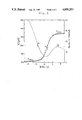
- FIG. 3 is a graph showing the capacitance vs. voltage characteristics of a structure of the present invention.
- the surface of the compound semiconductor substrate is passivated by forming a very thin layer of anionic nitride that is free of detectable amounts of cationic nitride on the surface of the compound semiconductor.
- a layer of insulating material is deposited on the anionic nitride layer.
- the interface between the insulating material and the substrate has a very low density of states so that the Fermi level may be swept through the entire band gap.
- a substrate of bulk gallium arsenide is passivated in accordance with the invention by first annealing the substrate in a temperature range of 300-500° C.
- the substrate is preferably annealed in a nitrogen or argon atmosphere.
- the gallium arsenide substrate surface prior to annealing is composed of arsenic oxide and gallium oxide. After the annealing, the surface layer becomes arsenic rich and contains gallium oxide and small amounts of arsenic oxide. The majority of the arsenic oxide will be transformed into elemental arsenic in accordance with the following formula:
- the gallium oxide formed from the above reaction combines with the gallium oxide already present on the surface to form a layer containing a large amount of gallium oxide with arsenic and small amounts of arsenic oxide.
- the resulting structure is then subjected to a wet etch in dilute HCl which strips the gallium oxide and the arsenic oxide leaving an extremely thin layer of arsenic.
- the layer of arsenic is on the order of one monolayer.
- the substrate is transferred in air which causes oxygen to be chemisorbed by the substrate. It is likely that the oxygen is chemisorbed in the arsenic layer. Although oxygen is chemisorbed, there are no arsenic or gallium oxides present on the substrate.
- the substrate is then introduced into a plasma reactor where it is subjected to a plasma cleaning in hydrogen at a temperature in the range of 150° to 300° C.
- the H 2 plasma cleaning is preferably performed at low pressure and low voltage.
- the H 2 plasma is performed in a range of 1 to 10 mTorr and at a voltage in the range of -50 to -250 volts dc.
- the H 2 plasma reduces the GaAs surface by stripping any chemisorbed oxygen from the surface.
- the H 2 plasma is an RF plasma process.
- the surface layer is free from gallium and arsenic oxides, however, the elemental arsenic is not depleted Thus, the monolayer of arsenic on the surface of the gallium arsenic substrate remains.
- the substrate is then subjected to a RF plasma cleaning in N 2 , also preferably at low pressure and low voltage.
- N 2 plasma conditions are identical to the range of conditions set forth above for the H 2 plasma.
- the surface of the substrate after the H 2 plasma containing the monolayer of elemental arsenic is highly reactive.
- the RF nitridization will passivate the GaAs surface by forming a layer of arsenic nitride. Since nitrogen has the same valence as arsenic, As-N bonds will form. Thus, the elemental arsenic is passivated which has the result of reducing the surface charge of the structure.
- the charge will be reduced from 10 13 eV/cm 2 to 10 11 eV/cm 2 .
- the AsN layer is free from any detectable amounts of gallium nitride.
- the passivated gallium arsenide substrate is provided with a surface that is suitable for deposition of an insulating material.
- the gallium arsenide surface is passivated by the AsN layer to the extent that the density of states present at the semiconductor/insulator interface is low enough to permit the Fermi level to be swept through the entire band gap.
- the structure 10 includes a gallium arsenide substrate 12 having a first major surface 14 and a second major surface 16.
- a metallic contact such as, AuGeNi, may be formed on the surface 16 during the initial annealing step.
- An insulation layer 22 is deposited onto the arsenic nitride layer 20, which in the illustrative embodiment in FIG. 1 is gallium oxide.
- a gate contact 24 is deposited onto the oxide layer 22 to complete the structure.
- the gallium oxide layer 22 is preferably deposited by electron beam evaporation in a low voltage, low pressure O 2 plasma.
- the scheme for E-beam evaporation includes a chamber 26 having a cathode 28 coupled to an RF source 30.
- a passivated gallium arsenide substrate 32 is positioned in contact with the cathode 28.
- a crucible 34 containing pure gallium 36 is placed in the chamber and an O 2 plasma is created by introducing oxygen through line 38, which causes Ga 2 O 3 to be reactively deposited onto the passivated gallium arsenide substrate.
- the substrate is passivated in situ in chamber 26 by first creating a hydrogen plasma by opening line 40 and then creating a nitrogen plasma by closing line 40 and opening line 42.
- the pressure and voltage ranges for the deposition of the oxide are preferably 1 to 10 mTorr and -50 to -250 volts dc, respectively. Temperature conditions are in the range of 24 to 260° C.
- the gallium oxide layer is uniform and transparent and can be grown to a thickness of 1000 angstroms or more. Sample oxides have been deposited at thicknesses ranging from 950 to 1100 angstroms across a 51 mm wafer. Ellipsometry analysis shows that the oxides have an index of refraction in the range between 1.50 to 1.90.
- a substrate of bulk gallium arsenide was annealed at 450° C.
- An substrate of bulk AuGeNi metallic contact was alloyed during this step on one surface of the substrate.
- an x-ray photospectroscopy analysis revealed that the surface contained substantial amounts of gallium oxide together with small amounts of arsenic oxide and elemental arsenic.
- the substrate was then dipped in a dilute HCl solution to etch the gallium and arsenic oxides from the surface. XPS tests indicated that no oxides were present with only a very thin layer of arsenic remaining. After the etch, the substrate was transferred in air which caused oxygen to be chemisorbed on the substrate.
- XPS analysis showed no arsenic or gallium oxide present.
- the substrate was then introduced into a plasma reactor where it was subjected to the plasma cleaning in hydrogen with the substrate held at a temperature of 200° C.
- the hydrogen was at a pressure of 5 mTorr and the voltage applied was -150 volts dc.
- the H 2 plasma cleaning was performed for one minute.
- XPS analysis of the substrate after the H 2 cleaning indicated no oxygen present.
- the substrate was then subjected to a plasma nitridization in N 2 with the substrate being held at a temperature of 200° C.
- the pressure was again 5 mTorr and the voltage -150 volts dc.
- the N 2 plasma cleaning was also performed for one minute.
- the XPS results showed a shoulder indicating arsenic nitride.
- a layer of Ga 2 O 3 was deposited by electron beam evaporation of pure gallium through a low voltage, low pressure O 2 plasma.
- the plasma pressure was 2 mTorr at -100 volts dc.
- the temperature was 24° C.
- Ellipsometry analysis indicated that the oxide had an index of refraction of 1.58.
- the thickness of the oxide layer was approximately 75 nanometers. Auger analysis indicated only the presence of gallium and oxygen with no arsenic.
- the gallium oxide deposition should preferably take place in situ to prevent interface contamination due to air exposure. After the deposition of the oxide, a thin AsN layer remains at the interface. A gold contact was deposited onto the gallium oxide surface to form an MOS diode and a bias voltage was applied to the structure.
- ⁇ i is found to be 8.3.
- the minimum capacitance Cmin is evaluated according to: ##EQU1## Where, ⁇ s is equal to 12.9, N d is the dopant and is equal to 2 ⁇ 10 17 cm -3 and n is the intrinsic carrier concentration and is equal to 1.79 ⁇ 10 6 cm -3 , C min is found to be 205 pF. which is very close to the capacitance measured from FIG. 3.
- devices for integrated circuits may be fabricated having a gallium oxide interlevel insulator due to its low dielectric constant.
- the gallium oxide will not etch in a F + containing plasma so that the oxide will make an excellent reactive ion etching mask.
- the present invention provides a method for passivating the surface of a compound semiconductor in which the surface is pretreated with an annealing step and a wet etch step which leaves a monolayer of arsenic on the surface.
- the substrate with the monolayer of arsenic is then subjected to an H 2 plasma cleaning and a N 2 plasma cleaning resulting in the substrate having an arsenic nitride layer that is very thin.
- a layer of insulating material such as gallium oxide is then deposited.
- the passivation results in the density of interface states being extremely low which allows the Fermi level to be swept through entire band gap.
Landscapes
- Formation Of Insulating Films (AREA)
- Cleaning Or Drying Semiconductors (AREA)
- Drying Of Semiconductors (AREA)
Priority Applications (5)
| Application Number | Priority Date | Filing Date | Title |
|---|---|---|---|
| US07/221,686 US4859253A (en) | 1988-07-20 | 1988-07-20 | Method for passivating a compound semiconductor surface and device having improved semiconductor-insulator interface |
| EP89108122A EP0351505B1 (fr) | 1988-07-20 | 1989-05-05 | Procédé pour passiver une surface de semiconducteur composé |
| DE68919561T DE68919561T2 (de) | 1988-07-20 | 1989-05-05 | Verfahren zur Oberflächenpassivierung eines zusammengesetzten Halbleiters. |
| CA000600747A CA1283490C (fr) | 1988-07-20 | 1989-05-25 | Methode de passivation de la surface d'un semiconducteur compose et dispositif a interface semiconducteur-isolant amelioree |
| JP1171776A JPH0714064B2 (ja) | 1988-07-20 | 1989-07-03 | 化合物半導体の表面をパッシベートする方法 |
Applications Claiming Priority (1)
| Application Number | Priority Date | Filing Date | Title |
|---|---|---|---|
| US07/221,686 US4859253A (en) | 1988-07-20 | 1988-07-20 | Method for passivating a compound semiconductor surface and device having improved semiconductor-insulator interface |
Publications (1)
| Publication Number | Publication Date |
|---|---|
| US4859253A true US4859253A (en) | 1989-08-22 |
Family
ID=22828894
Family Applications (1)
| Application Number | Title | Priority Date | Filing Date |
|---|---|---|---|
| US07/221,686 Expired - Lifetime US4859253A (en) | 1988-07-20 | 1988-07-20 | Method for passivating a compound semiconductor surface and device having improved semiconductor-insulator interface |
Country Status (5)
| Country | Link |
|---|---|
| US (1) | US4859253A (fr) |
| EP (1) | EP0351505B1 (fr) |
| JP (1) | JPH0714064B2 (fr) |
| CA (1) | CA1283490C (fr) |
| DE (1) | DE68919561T2 (fr) |
Cited By (27)
| Publication number | Priority date | Publication date | Assignee | Title |
|---|---|---|---|---|
| US4987095A (en) * | 1988-06-15 | 1991-01-22 | International Business Machines Corp. | Method of making unpinned oxide-compound semiconductor structures |
| US5021365A (en) * | 1986-06-16 | 1991-06-04 | International Business Machines Corporation | Compound semiconductor interface control using cationic ingredient oxide to prevent fermi level pinning |
| WO1992009108A1 (fr) * | 1990-11-16 | 1992-05-29 | United States Department Of Energy | Oxydation d'arseniure de gallium |
| US5223458A (en) * | 1990-12-18 | 1993-06-29 | Raytheon Company | Method of manufacturing a III-V semiconductor device using a self-biased substrate and a plasma containing an electronegative species |
| US5267437A (en) * | 1991-05-23 | 1993-12-07 | United Technologies Corporation | Dual mode rocket engine |
| US5438022A (en) * | 1993-12-14 | 1995-08-01 | At&T Global Information Solutions Company | Method for using low dielectric constant material in integrated circuit fabrication |
| US5464664A (en) * | 1992-06-16 | 1995-11-07 | At&T Ipm Corp. | Downstream ammonia plasma passivation of GaAs |
| US5597768A (en) * | 1996-03-21 | 1997-01-28 | Motorola, Inc. | Method of forming a Ga2 O3 dielectric layer |
| US5616947A (en) * | 1994-02-01 | 1997-04-01 | Matsushita Electric Industrial Co., Ltd. | Semiconductor device having an MIS structure |
| EP0863539A1 (fr) * | 1997-03-04 | 1998-09-09 | Motorola, Inc. | Structure d'interface isolant-semiconducteur composé et son procédé de fabrication |
| US5821171A (en) * | 1994-03-23 | 1998-10-13 | Lucent Technologies Inc. | Article comprising a gallium layer on a GaAs-based semiconductor, and method of making the article |
| US5902130A (en) * | 1997-07-17 | 1999-05-11 | Motorola, Inc. | Thermal processing of oxide-compound semiconductor structures |
| US5958519A (en) * | 1997-09-15 | 1999-09-28 | National Science Council | Method for forming oxide film on III-V substrate |
| US5962883A (en) * | 1994-03-23 | 1999-10-05 | Lucent Technologies Inc. | Article comprising an oxide layer on a GaAs-based semiconductor body |
| US6030453A (en) * | 1997-03-04 | 2000-02-29 | Motorola, Inc. | III-V epitaxial wafer production |
| US6140250A (en) * | 1996-05-27 | 2000-10-31 | Sony Corporation | Method for forming oxide film of semiconductor device, and oxide film forming apparatus capable of shortening pre-processing time for concentration measurement |
| US6445015B1 (en) | 2000-05-04 | 2002-09-03 | Osemi, Incorporated | Metal sulfide semiconductor transistor devices |
| US6451711B1 (en) * | 2000-05-04 | 2002-09-17 | Osemi, Incorporated | Epitaxial wafer apparatus |
| US6670651B1 (en) | 2000-05-04 | 2003-12-30 | Osemi, Inc. | Metal sulfide-oxide semiconductor transistor devices |
| US20040207029A1 (en) * | 2002-07-16 | 2004-10-21 | Braddock Walter David | Junction field effect metal oxide compound semiconductor integrated transistor devices |
| US20040206979A1 (en) * | 2002-06-06 | 2004-10-21 | Braddock Walter David | Metal oxide compound semiconductor integrated transistor devices |
| US6936900B1 (en) | 2000-05-04 | 2005-08-30 | Osemi, Inc. | Integrated transistor devices |
| US20070138506A1 (en) * | 2003-11-17 | 2007-06-21 | Braddock Walter D | Nitride metal oxide semiconductor integrated transistor devices |
| US20080282983A1 (en) * | 2003-12-09 | 2008-11-20 | Braddock Iv Walter David | High Temperature Vacuum Evaporation Apparatus |
| US20180108525A1 (en) * | 2016-10-14 | 2018-04-19 | Case Western Reserve University | Method for Forming a Thin Film Comprising an Ultrawide Bandgap Oxide Semiconductor |
| CN107993934A (zh) * | 2017-12-08 | 2018-05-04 | 中国科学院微电子研究所 | 增强氧化镓半导体器件欧姆接触的方法 |
| US12476156B2 (en) * | 2021-10-08 | 2025-11-18 | Denso Corporation | Semiconductor chip and method for manufacturing the same |
Families Citing this family (3)
| Publication number | Priority date | Publication date | Assignee | Title |
|---|---|---|---|---|
| RU2168237C2 (ru) * | 1999-05-11 | 2001-05-27 | Берковиц Владимир Леонидович | Способ получения нитридной пленки на поверхности полупроводниковых соединений а3в5 |
| JP4676046B2 (ja) * | 2000-05-10 | 2011-04-27 | 古河電気工業株式会社 | GaN系絶縁ゲート形電界効果トランジスタ |
| RU2370854C1 (ru) * | 2008-06-16 | 2009-10-20 | Физико-технический институт им. А.Ф. Иоффе РАН | СПОСОБ ПОЛУЧЕНИЯ НИТРИДНОЙ ПЛЕНКИ НА ПОВЕРХНОСТИ ГЕТЕРОСТРУКТУРЫ НА ОСНОВЕ GaSb |
Citations (14)
| Publication number | Priority date | Publication date | Assignee | Title |
|---|---|---|---|---|
| US3411938A (en) * | 1964-08-07 | 1968-11-19 | Sperry Rand Corp | Copper substrate cleaning and vapor coating method |
| US3849276A (en) * | 1971-03-19 | 1974-11-19 | Ibm | Process for forming reactive layers whose thickness is independent of time |
| US4058638A (en) * | 1974-12-19 | 1977-11-15 | Texas Instruments Incorporated | Method of optical thin film coating |
| US4297176A (en) * | 1979-03-09 | 1981-10-27 | National Research Development Corporation | Surface passivation of compound semiconductors |
| US4336277A (en) * | 1980-09-29 | 1982-06-22 | The Regents Of The University Of California | Transparent electrical conducting films by activated reactive evaporation |
| US4361114A (en) * | 1980-10-06 | 1982-11-30 | Optical Coating Laboratory, Inc. | Method and apparatus for forming thin film oxide layers using reactive evaporation techniques |
| US4436770A (en) * | 1978-04-01 | 1984-03-13 | Budda Hajia Handotai Kenkyu Shinkokai | Oxynitride film and its manufacturing method |
| US4514437A (en) * | 1984-05-02 | 1985-04-30 | Energy Conversion Devices, Inc. | Apparatus for plasma assisted evaporation of thin films and corresponding method of deposition |
| US4526802A (en) * | 1983-03-31 | 1985-07-02 | Clarion Co., Ltd. | Film deposition equipment |
| GB2158104A (en) * | 1984-05-04 | 1985-11-06 | Diesel Kiki Co | Method for producing a thin film |
| US4597825A (en) * | 1982-11-10 | 1986-07-01 | International Business Machines Corporation | Intermediate passivation and cleaning of compound semiconductor surfaces |
| JPS61196201A (ja) * | 1985-02-26 | 1986-08-30 | Canon Inc | 低温蒸着成膜法 |
| US4645683A (en) * | 1984-10-09 | 1987-02-24 | U.S. Philips Corporation | Method of manufacturing a semiconductor device |
| US4706377A (en) * | 1986-01-30 | 1987-11-17 | United Technologies Corporation | Passivation of gallium arsenide by nitrogen implantation |
Family Cites Families (1)
| Publication number | Priority date | Publication date | Assignee | Title |
|---|---|---|---|---|
| JPS5856425A (ja) * | 1981-09-30 | 1983-04-04 | Nippon Telegr & Teleph Corp <Ntt> | 化合物半導体結晶上の絶縁膜の形成法 |
-
1988
- 1988-07-20 US US07/221,686 patent/US4859253A/en not_active Expired - Lifetime
-
1989
- 1989-05-05 DE DE68919561T patent/DE68919561T2/de not_active Expired - Fee Related
- 1989-05-05 EP EP89108122A patent/EP0351505B1/fr not_active Expired - Lifetime
- 1989-05-25 CA CA000600747A patent/CA1283490C/fr not_active Expired - Lifetime
- 1989-07-03 JP JP1171776A patent/JPH0714064B2/ja not_active Expired - Lifetime
Patent Citations (14)
| Publication number | Priority date | Publication date | Assignee | Title |
|---|---|---|---|---|
| US3411938A (en) * | 1964-08-07 | 1968-11-19 | Sperry Rand Corp | Copper substrate cleaning and vapor coating method |
| US3849276A (en) * | 1971-03-19 | 1974-11-19 | Ibm | Process for forming reactive layers whose thickness is independent of time |
| US4058638A (en) * | 1974-12-19 | 1977-11-15 | Texas Instruments Incorporated | Method of optical thin film coating |
| US4436770A (en) * | 1978-04-01 | 1984-03-13 | Budda Hajia Handotai Kenkyu Shinkokai | Oxynitride film and its manufacturing method |
| US4297176A (en) * | 1979-03-09 | 1981-10-27 | National Research Development Corporation | Surface passivation of compound semiconductors |
| US4336277A (en) * | 1980-09-29 | 1982-06-22 | The Regents Of The University Of California | Transparent electrical conducting films by activated reactive evaporation |
| US4361114A (en) * | 1980-10-06 | 1982-11-30 | Optical Coating Laboratory, Inc. | Method and apparatus for forming thin film oxide layers using reactive evaporation techniques |
| US4597825A (en) * | 1982-11-10 | 1986-07-01 | International Business Machines Corporation | Intermediate passivation and cleaning of compound semiconductor surfaces |
| US4526802A (en) * | 1983-03-31 | 1985-07-02 | Clarion Co., Ltd. | Film deposition equipment |
| US4514437A (en) * | 1984-05-02 | 1985-04-30 | Energy Conversion Devices, Inc. | Apparatus for plasma assisted evaporation of thin films and corresponding method of deposition |
| GB2158104A (en) * | 1984-05-04 | 1985-11-06 | Diesel Kiki Co | Method for producing a thin film |
| US4645683A (en) * | 1984-10-09 | 1987-02-24 | U.S. Philips Corporation | Method of manufacturing a semiconductor device |
| JPS61196201A (ja) * | 1985-02-26 | 1986-08-30 | Canon Inc | 低温蒸着成膜法 |
| US4706377A (en) * | 1986-01-30 | 1987-11-17 | United Technologies Corporation | Passivation of gallium arsenide by nitrogen implantation |
Non-Patent Citations (24)
| Title |
|---|
| Boher et al., H 2 Plasma Induced Effects on GaAs Examined by Photoluminescence, Ellipsometry and X ray Photoemission, Proceedings of the Fourteenth International Symposium, Greece, Sep. 1987. * |
| Boher et al., H2 Plasma Induced Effects on GaAs Examined by Photoluminescence, Ellipsometry and X-ray Photoemission, Proceedings of the Fourteenth International Symposium, Greece, Sep. 1987. |
| Boher et al., Structural and Electrical Properties of Silicon Nitride Films Prepared by Multipolar Plasma enhanced Deposition, J. Appl. Phys. 63(5), Mar. 1988, pp. 1464 1472. * |
| Boher et al., Structural and Electrical Properties of Silicon Nitride Films Prepared by Multipolar Plasma-enhanced Deposition, J. Appl. Phys. 63(5), Mar. 1988, pp. 1464-1472. |
| Chang et al., Plasma Oxidation of GaAs, Applied Physics Letters, vol. 29, No. 1, Jul. 1976, pp. 56 58. * |
| Chang et al., Plasma Oxidation of GaAs, Applied Physics Letters, vol. 29, No. 1, Jul. 1976, pp. 56-58. |
| Chesler et al., dc Plasma Anodization of GaAs, Appl. Phys. Lett. 32(1) Jan. 1978, pp. 60 62. * |
| Chesler et al., dc Plasma Anodization of GaAs, Appl. Phys. Lett. 32(1) Jan. 1978, pp. 60-62. |
| Friedel et al., Photoemission Study of the Passive of GaAs in a Nitrogen Multipolar Plasma, Philosophical Magazine B, 1987, vol. 55, No. 6, pp. 711 719. * |
| Friedel et al., Photoemission Study of the Passive of GaAs in a Nitrogen Multipolar Plasma, Philosophical Magazine B, 1987, vol. 55, No. 6, pp. 711-719. |
| Friedel et al., Study of the Interaction of Plasmas with III V Semiconductor Surfaces, Application to Passivation, Surface Science 168 (1986), pp. 635 644. * |
| Friedel et al., Study of the Interaction of Plasmas with III-V Semiconductor Surfaces, Application to Passivation, Surface Science 168 (1986), pp. 635-644. |
| Friedel, P., Interactions Between Molecular Hydrogen and Molecular Nitrogen Plasmas and a Gallium Arsenide (100) Surface: Chemical and Electronic Properties, Appl. Phys. Lett., 42(6), pp. 509 511. * |
| Friedel, P., Interactions Between Molecular Hydrogen and Molecular Nitrogen Plasmas and a Gallium Arsenide (100) Surface: Chemical and Electronic Properties, Appl. Phys. Lett., 42(6), pp. 509-511. |
| Gourrier, S., Core Level Photoemission Study of the Interaction of Plasmas with Real Gallium Arsenide (100) Surfaces, Surf. Sci., 152 153(2), pp. 1147 1152. * |
| Gourrier, S., Core Level Photoemission Study of the Interaction of Plasmas with Real Gallium Arsenide (100) Surfaces, Surf. Sci., 152-153(2), pp. 1147-1152. |
| Koshiga et al., The Anodic Oxidation of GaAs in an Oxygen Plasma Generated by A D.C. Electrical Discharge, Thin Solid Films 56 (1979), pp. 39 49. * |
| Koshiga et al., The Anodic Oxidation of GaAs in an Oxygen Plasma Generated by A D.C. Electrical Discharge, Thin Solid Films 56 (1979), pp. 39-49. |
| Sugano et al., Oxidation of GaAs P Surface by Oxygen Plasma and Properties of Oxide Film., J. Electrochem. Soc.: Solid State Science and Technology, vol. 121, No. 1, Jan. 1974, pp. 113 118. * |
| Sugano et al., Oxidation of GaAs P Surface by Oxygen Plasma and Properties of Oxide Film., J. Electrochem. Soc.: Solid-State Science and Technology, vol. 121, No. 1, Jan. 1974, pp. 113-118. |
| Weinreich, Oxide Films Grown on GaAs in Oxygen Plasma, Communications, pp. 2924 2926. * |
| Weinreich, Oxide Films Grown on GaAs in Oxygen Plasma, Communications, pp. 2924-2926. |
| Yokoyama et al., Low Termperature Plasma Oxidation of GaAs, Appl. Phys. Lett. 32(1), Jan. 1978, pp. 58 60. * |
| Yokoyama et al., Low-Termperature Plasma Oxidation of GaAs, Appl. Phys. Lett. 32(1), Jan. 1978, pp. 58-60. |
Cited By (39)
| Publication number | Priority date | Publication date | Assignee | Title |
|---|---|---|---|---|
| US5021365A (en) * | 1986-06-16 | 1991-06-04 | International Business Machines Corporation | Compound semiconductor interface control using cationic ingredient oxide to prevent fermi level pinning |
| US4987095A (en) * | 1988-06-15 | 1991-01-22 | International Business Machines Corp. | Method of making unpinned oxide-compound semiconductor structures |
| WO1992009108A1 (fr) * | 1990-11-16 | 1992-05-29 | United States Department Of Energy | Oxydation d'arseniure de gallium |
| US5223458A (en) * | 1990-12-18 | 1993-06-29 | Raytheon Company | Method of manufacturing a III-V semiconductor device using a self-biased substrate and a plasma containing an electronegative species |
| US5267437A (en) * | 1991-05-23 | 1993-12-07 | United Technologies Corporation | Dual mode rocket engine |
| US5464664A (en) * | 1992-06-16 | 1995-11-07 | At&T Ipm Corp. | Downstream ammonia plasma passivation of GaAs |
| US6522006B1 (en) | 1993-12-14 | 2003-02-18 | Hyundai Electronics America Inc. | Low dielectric constant material in integrated circuit |
| US5438022A (en) * | 1993-12-14 | 1995-08-01 | At&T Global Information Solutions Company | Method for using low dielectric constant material in integrated circuit fabrication |
| US6522005B1 (en) | 1993-12-14 | 2003-02-18 | Hyundai Electronics America Inc. | Integrated circuit device comprising low dielectric constant material for reduced cross talk |
| US6448653B1 (en) | 1993-12-14 | 2002-09-10 | Hyundai Electronics America | Method for using low dielectric constant material in integrated circuit fabrication |
| US6504249B1 (en) | 1993-12-14 | 2003-01-07 | Hyundai Electronics America Inc. | Integrated circuit device with reduced cross talk |
| US6208029B1 (en) | 1993-12-14 | 2001-03-27 | Hyundai Electronics America | Integrated circuit device with reduced cross talk |
| US6504250B1 (en) | 1993-12-14 | 2003-01-07 | Hyundai Electronics America Inc. | Integrated circuit device with reduced cross talk |
| US5616947A (en) * | 1994-02-01 | 1997-04-01 | Matsushita Electric Industrial Co., Ltd. | Semiconductor device having an MIS structure |
| US5821171A (en) * | 1994-03-23 | 1998-10-13 | Lucent Technologies Inc. | Article comprising a gallium layer on a GaAs-based semiconductor, and method of making the article |
| US5962883A (en) * | 1994-03-23 | 1999-10-05 | Lucent Technologies Inc. | Article comprising an oxide layer on a GaAs-based semiconductor body |
| US5597768A (en) * | 1996-03-21 | 1997-01-28 | Motorola, Inc. | Method of forming a Ga2 O3 dielectric layer |
| US6140250A (en) * | 1996-05-27 | 2000-10-31 | Sony Corporation | Method for forming oxide film of semiconductor device, and oxide film forming apparatus capable of shortening pre-processing time for concentration measurement |
| EP0863539A1 (fr) * | 1997-03-04 | 1998-09-09 | Motorola, Inc. | Structure d'interface isolant-semiconducteur composé et son procédé de fabrication |
| US6030453A (en) * | 1997-03-04 | 2000-02-29 | Motorola, Inc. | III-V epitaxial wafer production |
| US5902130A (en) * | 1997-07-17 | 1999-05-11 | Motorola, Inc. | Thermal processing of oxide-compound semiconductor structures |
| US5958519A (en) * | 1997-09-15 | 1999-09-28 | National Science Council | Method for forming oxide film on III-V substrate |
| US20060076630A1 (en) * | 2000-05-04 | 2006-04-13 | Braddock Walter D Iv | Integrated Transistor devices |
| US7190037B2 (en) | 2000-05-04 | 2007-03-13 | Osemi, Inc. | Integrated transistor devices |
| US6670651B1 (en) | 2000-05-04 | 2003-12-30 | Osemi, Inc. | Metal sulfide-oxide semiconductor transistor devices |
| US6445015B1 (en) | 2000-05-04 | 2002-09-03 | Osemi, Incorporated | Metal sulfide semiconductor transistor devices |
| US6451711B1 (en) * | 2000-05-04 | 2002-09-17 | Osemi, Incorporated | Epitaxial wafer apparatus |
| US6936900B1 (en) | 2000-05-04 | 2005-08-30 | Osemi, Inc. | Integrated transistor devices |
| US6989556B2 (en) | 2002-06-06 | 2006-01-24 | Osemi, Inc. | Metal oxide compound semiconductor integrated transistor devices with a gate insulator structure |
| US20040206979A1 (en) * | 2002-06-06 | 2004-10-21 | Braddock Walter David | Metal oxide compound semiconductor integrated transistor devices |
| US7187045B2 (en) | 2002-07-16 | 2007-03-06 | Osemi, Inc. | Junction field effect metal oxide compound semiconductor integrated transistor devices |
| US20040207029A1 (en) * | 2002-07-16 | 2004-10-21 | Braddock Walter David | Junction field effect metal oxide compound semiconductor integrated transistor devices |
| US20070138506A1 (en) * | 2003-11-17 | 2007-06-21 | Braddock Walter D | Nitride metal oxide semiconductor integrated transistor devices |
| US20080282983A1 (en) * | 2003-12-09 | 2008-11-20 | Braddock Iv Walter David | High Temperature Vacuum Evaporation Apparatus |
| US20180108525A1 (en) * | 2016-10-14 | 2018-04-19 | Case Western Reserve University | Method for Forming a Thin Film Comprising an Ultrawide Bandgap Oxide Semiconductor |
| US10593544B2 (en) * | 2016-10-14 | 2020-03-17 | Case Westen Reverse University | Method for forming a thin film comprising an ultrawide bandgap oxide semiconductor |
| CN107993934A (zh) * | 2017-12-08 | 2018-05-04 | 中国科学院微电子研究所 | 增强氧化镓半导体器件欧姆接触的方法 |
| CN107993934B (zh) * | 2017-12-08 | 2020-09-11 | 中国科学院微电子研究所 | 增强氧化镓半导体器件欧姆接触的方法 |
| US12476156B2 (en) * | 2021-10-08 | 2025-11-18 | Denso Corporation | Semiconductor chip and method for manufacturing the same |
Also Published As
| Publication number | Publication date |
|---|---|
| CA1283490C (fr) | 1991-04-23 |
| JPH0714064B2 (ja) | 1995-02-15 |
| EP0351505A2 (fr) | 1990-01-24 |
| JPH0258332A (ja) | 1990-02-27 |
| EP0351505A3 (fr) | 1991-03-27 |
| DE68919561D1 (de) | 1995-01-12 |
| DE68919561T2 (de) | 1995-05-24 |
| EP0351505B1 (fr) | 1994-11-30 |
Similar Documents
| Publication | Publication Date | Title |
|---|---|---|
| US4859253A (en) | Method for passivating a compound semiconductor surface and device having improved semiconductor-insulator interface | |
| US6404027B1 (en) | High dielectric constant gate oxides for silicon-based devices | |
| CA2136581C (fr) | Fines pellicules d'oxyde de gallium | |
| US6136654A (en) | Method of forming thin silicon nitride or silicon oxynitride gate dielectrics | |
| EP1001468A1 (fr) | Couche d'oxyde des terres rares sur un corps semi-conducteur à base de GaAs ou GaN | |
| US6613677B1 (en) | Long range ordered semiconductor interface phase and oxides | |
| US4645683A (en) | Method of manufacturing a semiconductor device | |
| EP0863542A2 (fr) | Plaquette epitaxiée III-V | |
| US5902130A (en) | Thermal processing of oxide-compound semiconductor structures | |
| Batey et al. | Plasma-enhanced CVD of high quality insulating films | |
| US4987095A (en) | Method of making unpinned oxide-compound semiconductor structures | |
| EP0216285B1 (fr) | Procédé de traitement thermique d'un substrat semi-conducteur composite | |
| Lorenz et al. | Characterization of low temperature SiO2 and Si3N4 films deposited by plasma enhanced evaporation | |
| US5086321A (en) | Unpinned oxide-compound semiconductor structures and method of forming same | |
| US6451711B1 (en) | Epitaxial wafer apparatus | |
| Viktorovitch | Interface Properties of InP‐Dielectric Systems | |
| Hu et al. | Electron cyclotron resonance plasma process for InP passivation | |
| US5610098A (en) | N-INP Schottky diode structure and a method of making the same | |
| WO2003063227A2 (fr) | Procede de passivation de la surface d'un semi-conducteur iii-v | |
| Bhat et al. | Reactive ion beam deposition of aluminum nitride thin films | |
| Pan et al. | Properties of thin LPCVD silicon oxynitride films | |
| Besland et al. | Optimized SiO2/InP structures prepared by electron cyclotron resonance plasma | |
| US6359294B1 (en) | Insulator-compound semiconductor interface structure | |
| JP3399624B2 (ja) | 水素含有無定形炭素の製造方法 | |
| Santinelli et al. | Ion beam enhanced deposition of AINxOy alloys on InP |
Legal Events
| Date | Code | Title | Description |
|---|---|---|---|
| AS | Assignment |
Owner name: INTERNATIONAL BUSINESS MACHINES CORPORATION, ARMON Free format text: ASSIGNMENT OF ASSIGNORS INTEREST.;ASSIGNORS:BUCHANAN, DOUGLAS A.;CALLEGARI, ALESSANDRO C.;REEL/FRAME:004942/0358;SIGNING DATES FROM 19880805 TO 19880831 Owner name: INTERNATIONAL BUSINESS MACHINES CORPORATION, A COR Free format text: ASSIGNMENT OF ASSIGNORS INTEREST;ASSIGNORS:BUCHANAN, DOUGLAS A.;CALLEGARI, ALESSANDRO C.;SIGNING DATES FROM 19880805 TO 19880831;REEL/FRAME:004942/0358 |
|
| STCF | Information on status: patent grant |
Free format text: PATENTED CASE |
|
| CC | Certificate of correction | ||
| CC | Certificate of correction | ||
| FEPP | Fee payment procedure |
Free format text: PAYOR NUMBER ASSIGNED (ORIGINAL EVENT CODE: ASPN); ENTITY STATUS OF PATENT OWNER: LARGE ENTITY |
|
| FPAY | Fee payment |
Year of fee payment: 4 |
|
| FPAY | Fee payment |
Year of fee payment: 8 |
|
| FEPP | Fee payment procedure |
Free format text: PAYER NUMBER DE-ASSIGNED (ORIGINAL EVENT CODE: RMPN); ENTITY STATUS OF PATENT OWNER: LARGE ENTITY |
|
| FEPP | Fee payment procedure |
Free format text: PAYOR NUMBER ASSIGNED (ORIGINAL EVENT CODE: ASPN); ENTITY STATUS OF PATENT OWNER: LARGE ENTITY |
|
| FPAY | Fee payment |
Year of fee payment: 12 |