US4900975A - Target of image pickup tube having an amorphous semiconductor laminate - Google Patents
Target of image pickup tube having an amorphous semiconductor laminate Download PDFInfo
- Publication number
- US4900975A US4900975A US07/067,229 US6722987A US4900975A US 4900975 A US4900975 A US 4900975A US 6722987 A US6722987 A US 6722987A US 4900975 A US4900975 A US 4900975A
- Authority
- US
- United States
- Prior art keywords
- layer
- amorphous
- consisting essentially
- image pickup
- target
- Prior art date
- Legal status (The legal status is an assumption and is not a legal conclusion. Google has not performed a legal analysis and makes no representation as to the accuracy of the status listed.)
- Expired - Fee Related
Links
Images
Classifications
-
- H—ELECTRICITY
- H01—ELECTRIC ELEMENTS
- H01J—ELECTRIC DISCHARGE TUBES OR DISCHARGE LAMPS
- H01J31/00—Cathode ray tubes; Electron beam tubes
- H01J31/08—Cathode ray tubes; Electron beam tubes having a screen on or from which an image or pattern is formed, picked up, converted, or stored
- H01J31/26—Image pick-up tubes having an input of visible light and electric output
-
- H—ELECTRICITY
- H01—ELECTRIC ELEMENTS
- H01J—ELECTRIC DISCHARGE TUBES OR DISCHARGE LAMPS
- H01J29/00—Details of cathode-ray tubes or of electron-beam tubes of the types covered by group H01J31/00
- H01J29/02—Electrodes; Screens; Mounting, supporting, spacing or insulating thereof
- H01J29/10—Screens on or from which an image or pattern is formed, picked up, converted or stored
- H01J29/36—Photoelectric screens; Charge-storage screens
- H01J29/39—Charge-storage screens
- H01J29/45—Charge-storage screens exhibiting internal electric effects caused by electromagnetic radiation, e.g. photoconductive screen, photodielectric screen, photovoltaic screen
- H01J29/451—Charge-storage screens exhibiting internal electric effects caused by electromagnetic radiation, e.g. photoconductive screen, photodielectric screen, photovoltaic screen with photosensitive junctions
- H01J29/456—Charge-storage screens exhibiting internal electric effects caused by electromagnetic radiation, e.g. photoconductive screen, photodielectric screen, photovoltaic screen with photosensitive junctions exhibiting no discontinuities, e.g. consisting of uniform layers
-
- H—ELECTRICITY
- H01—ELECTRIC ELEMENTS
- H01J—ELECTRIC DISCHARGE TUBES OR DISCHARGE LAMPS
- H01J29/00—Details of cathode-ray tubes or of electron-beam tubes of the types covered by group H01J31/00
- H01J29/02—Electrodes; Screens; Mounting, supporting, spacing or insulating thereof
- H01J29/10—Screens on or from which an image or pattern is formed, picked up, converted or stored
- H01J29/36—Photoelectric screens; Charge-storage screens
- H01J29/39—Charge-storage screens
- H01J29/45—Charge-storage screens exhibiting internal electric effects caused by electromagnetic radiation, e.g. photoconductive screen, photodielectric screen, photovoltaic screen
Definitions
- This invention relates to a photoelectronic conversion element using an amorphous semiconductor material, and more particularly to a target of an image pickup tube having a photoelectronic conversion part suitable for use as an imaging device used in a television camera or the like.
- Amorphous silicon containing hydrogen (referred to hereinafter as "a-Si: H") has a high photoelectronic conversion efficiency and converts almost all of absorbed light into an electrical signal. It is an advantage of this a-Si: H that it can be doped with an impurity as in the case of crystalline semiconductors. It is another advantage of the a-Si: H that its film can be deposited at a low temperature on various substrates. Various devices making use of such advantages of the a-Si: H have been proposed hitherto.
- Japanese Patent Publication JP-B-57-046224 (1982) discloses an image pickup tube in which the a-Si: H is used to form a photoelectronic conversion film.
- the disclosed image pickup tube has various excellent features as follows: (1) the sensitivity for visible light is high; (2) the resolution is high; (3) it operates with a low lag and no sticking or no after image occurs after picking-up of still pictures for long period of time; and (4) it shows a high thermal stability.
- the above object is attained by forming a photoelectronic conversion part by laminating a layer of a-Si: H and a layer of an amorphous chalcogenide consisting essentially of selenium. In this laminate, it is essential to dispose the a-Si: H layer on the light receiving side of the photoelectronic conversion part.
- the a-Si: H has a high light absorption coefficient, and its optical bandgap can be suitably adjusted by controlling the condition of film formation and the content of hydrogen. Therefore, a thin film of a-Si: H can efficiently absorb signal light.
- an a-Si: H film having a thickness of only about 0.5 ⁇ m can sufficiently deal with signal light having wavelengths belonging to a visible wavelength range when the optical bandgap of the a-Si: H is selected to be about 1.7 eV.
- the photoelectronic conversion efficiency of the a-Si: H is high, the a-Si: H can absorb almost all of an incident optical signal and efficiently convert the optical input into photocarriers.
- amorphous selenium when compared with the a-Si: H, amorphous selenium has a higher ⁇ (mobility lifetime) product of holes, has a smaller electrical susceptibility and has a higher dark conductivity. Further, although the amorphous selenium absorbs soft X-rays and other radiant rays, it is hardly damaged by those rays, and its film can be formed by deposition at low temperatures. Therefore, a film of the amorphous selenium can be deposited on a layer of the a-Si: H without any possibility of damaging the underlying a-Si: H layer.
- a photo-electronic conversion part of multilayered structure in which its light receiving side is formed of a thin film consisting essentially of a-Si: H, and its side scanned with an electron beam to read an optical input signal is formed of a film consisting essentially of amorphous selenium, is used as a target of an image pickup tube, such a target possesses the features of both of these materials and can operate with excellent operating characteristics which have not been exhibited hitherto.
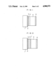
- FIG. 1 is a schematic sectional view of an embodiment of the photoelectronic conversion part of the image pickup tube according to the present invention.
- FIG. 2 is a schematic sectional view of a modification which includes an additionally provided intermediate layer.
- FIG. 3 is a schematic sectional view of the image pickup tube provided with the modification shown in FIG. 2.
- FIG. 4 is a graph showing the results of comparison of changes in the operating characteristics of a prior art image pickup tube having an a-Si: H layer only in its photoelectronic conversion part and an image pickup tube having an amorphous selenium layer combined with the a-Si: H layer in its photoelectronic conversion part according to the present invention when these tubes are continuously operated.
- FIG. 1 is a schematic sectional view of a photoelectronic conversion part of an image pickup tube embodying the present invention.
- the photoelectronic conversion part comprises a flat transparent glass substrate 1, a transparent electrode 2, a hole blocking layer 3, a photoconductive film 4 of a-Si: H, a layer 5 of an amorphous chalcogenide consisting essentially of selenium, and a layer 6 having a function of ensuring smooth landing of an electron beam.
- the transparent electrode 2 is preferably a very thin film of an oxide such as tin oxide or indium-tin oxide or a very thin light-transmitting film of an evaporated metal.
- the hole blocking layer 3 acts to block flow of holes from the transparent electrode 2 toward and into the photoconductive film 4 thereby suppressing the dark current to a low level and acts also to improve the photo-response.
- the layer 6 acts also to block injection of scanning electrons toward and into the amorphous chalcogenide layer 5 consisting essentially of amorphous selenium. Commonly, a porous layer of a material such as antimony trisulfide is used as this layer 6.
- the hole blocking layer 3 blocking flow of holes toward and into the photoconductive film 4 of a-Si: H is preferably a very thin film of a-Si: H doped with a donor impurity such as phosphorus, a material such as amorphous silicon nitride showing a high potential barrier against holes, or an electrical insulator such as silicon oxide.
- the thickness of the layer 3 is about 100 ⁇ .
- the thickness of the photoconductive layer 4 of a-Si: H is determined on the basis of the absorption factor of the a-Si:H so that light having a wavelength range corresponding to a camera used for imaging can be absorbed.
- the thickness of the layer 4 is preferably 0.1 to 1 ⁇ m, and more preferably 0.2 to 0.8 ⁇ m. When this layer 4 has an excessively large thickness, the number of photo-excited carriers trapped in the layer of a-Si: H while travelling therein increases. After the light is cut off, the trapped carriers will be liberated again, resulting in the increasing of lag.
- the thickness of the amorphous chalcogenide layer 5 is preferably about 1 to 10 ⁇ m.
- the layer 5 is advantageously as thick as possible in the above range, because the overall electrostatic capacity of the photo-electronic conversion part is correspondingly decreased. Further, the layer 5 should be at least 1 ⁇ m thick in order to sufficiently absorb soft X-rays.
- the optical signal is almost entirely absorbed in the a-Si: H layer 4 and is converted into photocarriers.
- a voltage is applied in a direction which causes flow of holes from the transparent electrode 2 toward the electron beam scanning side. Therefore, among the photocarriers produced in the a-Si: H layer 4 electrons flow toward the transparent electrode 2 through the a-Si: H layer 4 having a high ⁇ product of electron mobility, while holes flow toward the electron beam scanning side through the amorphous selenium layer 5 having a high ⁇ product of hole.
- FIG. 3 is a schematic sectional view of the image pickup tube described above.
- the reference numeral 1 designates the target substrate according to the present invention.
- the tube has an envelope 8 and an electron gun, and the reference numeral 10 indicates schematically an electron beam. The detail of the target will be described later.
- the image pickup tube Because of the unique structure of the photo-electronic conversion part of the image pickup tube described above, an incident optical signal is very efficiently converted into an electrical signal by utilization of the high photoelectronic conversion efficiency of the a-Si: layer 4. Therefore, the image pickup tube operates with a high sensitivity, and its operating characteristics are not degraded in spite of a long time of use since radiation generated in the electron gun 9 is absorbed by the amorphous selenium layer 5.
- holes generated in response to an optical input signal must be kept stored during the period of time of scanning with the electron beam.
- the charge pattern provided by the optical signal is stored though the amorphous selenium layer 5 having a high electrical resistance.
- the electrostatic capacity of the photoconductive film 4 can be made smaller than when the a-Si: H is singly used, and this is advantageous when a fast photo-response is desired.
- a photoelectronic conversion part of an image pickup tube has a multilayered structure provided by laminating a layer 5 of an amorphous chalcogenide on a photoconductive layer 4 of a-Si: H.
- a III-group element or a V-group element in an amount of about 0.5 to several-hundred ppm may be added to the photoconductive a-Si: H layer 4 thereby improving the mobility of carriers, or arsenic acting to suppress crystallization of selenium may be added in an amount of several percent by weight to the amorphous selenium layer 5.
- arsenic acting to suppress crystallization of selenium may be added in an amount of several percent by weight to the amorphous selenium layer 5.
- FIG. 2 shows the structure of the photoelectronic conversion part including the intermediate layer 7.
- the energy band structure can be changed by mixing, for example, germanium, carbon, tin or nitrogen in silicon thereby changing the composition.
- the intermediate layer 7 is formed of a material such as amorphous selenium
- addition of, for example, bismuth, cadmium, bismuth chalcogenide, cadmium chalcogenide, tellurium or tin to the amorphous selenium is effective for changing the energy band structure.
- the internal field strength in the hole layer can be changed by adding to the tetrahedral amorphous material a very small amount of a III-group or V-group element which can modify the conductivity type in the vicinity of the interface.
- the intermediate layer 7 is formed of a material such as amorphous selenium, it is effective to add an impurity which forms negative space charges, such as arsenic, germanium, antimony, indium, gallium or their chalcogenide, sulfur, chlorine, iodine, bromine, copper oxide, indium oxide, selenium oxide, vanadium pentoxide, molybdenum oxide, tungsten oxide, gallium fluoride or indium fluoride.
- an impurity which forms negative space charges such as arsenic, germanium, antimony, indium, gallium or their chalcogenide, sulfur, chlorine, iodine, bromine, copper oxide, indium oxide, selenium oxide, vanadium pentoxide, molybdenum oxide,
- FIG. 1 is a schematic sectional view of a target of an image pickup tube.
- a transparent, electrical conductive film 2 of tin oxide is deposited on a glass substrate 1 by a method well known in the art.
- This transparent conductive film 2 may be that usually deposited on a substrate of a conversion part of a convertional image pickup tube.
- a film 3 of silicon oxide about 100 ⁇ thick acting as a hole blocking layer and a photoconductive film 4 of a-Si: H containing 5 ppm of boron and about 0.1 to 1.0 ⁇ m thick are deposited in the above order on the glass substrate 1 having the tin oxide layer 2 deposited thereon in the manner described above.
- the silicon oxide film 3 may be deposited by a reactive sputtering method well known in the art, and the a-Si: H film 4 may be deposited by a well-known method of decomposing and polymerizing a gaseous material such as monosilane or disilane by means of plasma discharge. Heat or light may be used in lieu of the plasma discharge.
- a layer 5 of amorphous selenium containing 2% by weight of arsenic and about 6 ⁇ m thick is deposited on the photoconductive a-Si: H film 4 in an evaporation apparatus, and a layer 6 of antimony trisulfide about 500 ⁇ thick is deposited on the amorphous selenium layer 5 while introducing an inert gas into the evaporation apparatus.
- the photoelectronic conversion part formed in the manner described above is incorporated in a pickup-tube glass envelope having an electron gun 9 assembled therein to complete an image pickup tube.
- the image pickup tube thus completed was operated by applying a voltage of +200 volts to the transparent electrode 2 relative to the cathode of the electron gun 9.
- the sensitivity was equivalent to an image pickup tube including a photoconductive a-Si: H film about 4 ⁇ m thick in its photoelectronic conversion part, and degraded operating characteristics such as a reduction of the sensitivity and an increase in the dark current were not observed even when the image pickup tube was continuously operated for a period of time of 10,000 hours.
- This Example has also a structure as shown in FIG. 1.
- a transparent electrode 2 a hole blocking layer 3 of silicon oxide, and a photoconductive layer 4 of a-Si: H are deposited in the above order on a glass substrate 1.
- a layer 6 of porous antimony trisulfide about 600 ⁇ thick is deposited on the layer 5.
- an applied voltage of about 100 volts was sufficient for fully achieving the required sensitivity of the image pickup tube, and the image pickup tube could stably operate with operating characteristics similar to those of the Example 1.
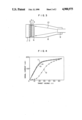
- FIG. 4 shows the relation between the target voltage and the signal current when the scanning electron beam is accelerated at a voltage as high as 800 volts.
- the curves 11 and 12 indicate the relation between the target voltage and the signal current of an prior art image pickup tube in which its target includes an a-Si: H layer only and does not include the amorphous selenium layer provided according to the present invention.
- the curve 11 represents the above relation at the beginning of the operation of the image pickup tube, while the curve 12 represents the above relation after continuous operation of the tube for 100 hours.
- the curves 13 and 14 indicate the relation between the target voltage and the signal current in the case of an image pickup tube to which the present invention is applied.
- the curve 13 represents the above relation at the beginning of the operation of the image pickup tube
- the curve 14 represents the above relation after continuous operation of the tube for 100 hours. It will be seen in FIG. 4 that the image pickup tube to which the present invention is applied can operate for a long period of time without appreciable degradation of its operating characteristics.
- This Example has a structure in which an intermediate layer is additionally provided in its photo-electric conversion part as shown in FIG. 2.
- a transparent electrode 2, a hole blocking layer 3, and a photoconductive a-Si: H layer 4 are deposited in the above order on a glass substrate 1.
- a film of a-Si: H containing 5 ppm of boron as its additive and about 200 ⁇ thick, and a film of a-Si: H containing 100 ppm of phosphorus as its additive and about 50 ⁇ thick are laminated in the above order on the layer 4.
- a layer 5 of amorphous selenium containing 2% by weight of arsenic and about 6 ⁇ m thick is deposited on the intermediate layer 7, and finally a beam landing layer 6 of antimony trisulfide is deposited on the layer 5.
- a transparent electrode 2, a hole blocking layer 3, and a photoconductive a-Si: H layer 4 are deposited in the above order on a glass substrate 1.
- a film of amorphous selenium containing 30% by weight of tellurium and about 200 ⁇ thick, and a film of amorphous selenium containing arsenic and about 500 ⁇ thick are laminated in the above order on the layer 4.
- its composition distribution is such that the concentration of arsenic decreases gradually from 20% to 2% in the direction of deposition of the film.
- a layer 5 of amorphous selenium containing 2% by weight of arsenic and about 6 ⁇ m thick is deposited on the intermediate layer 7, and finally beam landing layer 6 of antimony trisulfide is formed on the layer 6.
Landscapes
- Physics & Mathematics (AREA)
- Electromagnetism (AREA)
- Image-Pickup Tubes, Image-Amplification Tubes, And Storage Tubes (AREA)
- Light Receiving Elements (AREA)
Applications Claiming Priority (2)
| Application Number | Priority Date | Filing Date | Title |
|---|---|---|---|
| JP61-149553 | 1986-06-27 | ||
| JP61149553A JPH07101598B2 (ja) | 1986-06-27 | 1986-06-27 | 撮像管 |
Publications (1)
| Publication Number | Publication Date |
|---|---|
| US4900975A true US4900975A (en) | 1990-02-13 |
Family
ID=15477677
Family Applications (1)
| Application Number | Title | Priority Date | Filing Date |
|---|---|---|---|
| US07/067,229 Expired - Fee Related US4900975A (en) | 1986-06-27 | 1987-06-29 | Target of image pickup tube having an amorphous semiconductor laminate |
Country Status (5)
| Country | Link |
|---|---|
| US (1) | US4900975A (ja) |
| EP (1) | EP0251647B1 (ja) |
| JP (1) | JPH07101598B2 (ja) |
| KR (1) | KR910000904B1 (ja) |
| DE (1) | DE3784790T2 (ja) |
Cited By (11)
| Publication number | Priority date | Publication date | Assignee | Title |
|---|---|---|---|---|
| US5466613A (en) * | 1992-06-19 | 1995-11-14 | Nippon Hoso Kyokai | Method of manufacturing a camera device |
| US5892222A (en) * | 1996-04-18 | 1999-04-06 | Loral Fairchild Corporation | Broadband multicolor photon counter for low light detection and imaging |
| US20030230337A1 (en) * | 2002-03-29 | 2003-12-18 | Gaudiana Russell A. | Photovoltaic cells utilizing mesh electrodes |
| US20050067007A1 (en) * | 2001-11-08 | 2005-03-31 | Nils Toft | Photovoltaic element and production methods |
| US20060090791A1 (en) * | 2003-03-24 | 2006-05-04 | Russell Gaudiana | Photovoltaic cell with mesh electrode |
| US20070108398A1 (en) * | 2005-11-01 | 2007-05-17 | Fujifilm Corporation | Radiation image detector |
| US20070193621A1 (en) * | 2005-12-21 | 2007-08-23 | Konarka Technologies, Inc. | Photovoltaic cells |
| US20070224464A1 (en) * | 2005-03-21 | 2007-09-27 | Srini Balasubramanian | Dye-sensitized photovoltaic cells |
| US20070251570A1 (en) * | 2002-03-29 | 2007-11-01 | Konarka Technologies, Inc. | Photovoltaic cells utilizing mesh electrodes |
| US20080236657A1 (en) * | 2007-04-02 | 2008-10-02 | Christoph Brabec | Novel Electrode |
| US20090188547A1 (en) * | 2008-01-30 | 2009-07-30 | Fujifilm Corporation | Photoelectric conversion element and solid-state imaging device |
Citations (2)
| Publication number | Priority date | Publication date | Assignee | Title |
|---|---|---|---|---|
| US3984722A (en) * | 1973-05-21 | 1976-10-05 | Hitachi, Ltd. | Photoconductive target of an image pickup tube and method for manufacturing the same |
| US4419604A (en) * | 1980-04-25 | 1983-12-06 | Hitachi, Ltd. | Light sensitive screen |
Family Cites Families (5)
| Publication number | Priority date | Publication date | Assignee | Title |
|---|---|---|---|---|
| JPS56103477A (en) * | 1980-01-21 | 1981-08-18 | Hitachi Ltd | Photoelectric conversion element |
| JPS56132750A (en) * | 1980-03-24 | 1981-10-17 | Hitachi Ltd | Photoelectric converter and manufacture |
| DE3280112D1 (de) * | 1981-07-17 | 1990-03-15 | Kanegafuchi Chemical Ind | Amorpher halbleiter und photovoltaische einrichtung aus amorphem silizium. |
| JPS58194231A (ja) * | 1982-05-10 | 1983-11-12 | Hitachi Ltd | 撮像管 |
| JPS62262348A (ja) * | 1986-05-09 | 1987-11-14 | Hitachi Ltd | 撮像管タ−ゲツト |
-
1986
- 1986-06-27 JP JP61149553A patent/JPH07101598B2/ja not_active Expired - Lifetime
-
1987
- 1987-06-23 DE DE8787305562T patent/DE3784790T2/de not_active Expired - Fee Related
- 1987-06-23 EP EP87305562A patent/EP0251647B1/en not_active Expired - Lifetime
- 1987-06-27 KR KR1019870006578A patent/KR910000904B1/ko not_active Expired
- 1987-06-29 US US07/067,229 patent/US4900975A/en not_active Expired - Fee Related
Patent Citations (2)
| Publication number | Priority date | Publication date | Assignee | Title |
|---|---|---|---|---|
| US3984722A (en) * | 1973-05-21 | 1976-10-05 | Hitachi, Ltd. | Photoconductive target of an image pickup tube and method for manufacturing the same |
| US4419604A (en) * | 1980-04-25 | 1983-12-06 | Hitachi, Ltd. | Light sensitive screen |
Cited By (16)
| Publication number | Priority date | Publication date | Assignee | Title |
|---|---|---|---|---|
| US5466613A (en) * | 1992-06-19 | 1995-11-14 | Nippon Hoso Kyokai | Method of manufacturing a camera device |
| US5892222A (en) * | 1996-04-18 | 1999-04-06 | Loral Fairchild Corporation | Broadband multicolor photon counter for low light detection and imaging |
| US20050067007A1 (en) * | 2001-11-08 | 2005-03-31 | Nils Toft | Photovoltaic element and production methods |
| US20030230337A1 (en) * | 2002-03-29 | 2003-12-18 | Gaudiana Russell A. | Photovoltaic cells utilizing mesh electrodes |
| US7022910B2 (en) | 2002-03-29 | 2006-04-04 | Konarka Technologies, Inc. | Photovoltaic cells utilizing mesh electrodes |
| US20070251570A1 (en) * | 2002-03-29 | 2007-11-01 | Konarka Technologies, Inc. | Photovoltaic cells utilizing mesh electrodes |
| US20060090791A1 (en) * | 2003-03-24 | 2006-05-04 | Russell Gaudiana | Photovoltaic cell with mesh electrode |
| US20070131277A1 (en) * | 2003-03-24 | 2007-06-14 | Konarka Technologies, Inc. | Photovoltaic cell with mesh electrode |
| US20070224464A1 (en) * | 2005-03-21 | 2007-09-27 | Srini Balasubramanian | Dye-sensitized photovoltaic cells |
| US7649177B2 (en) * | 2005-11-01 | 2010-01-19 | Fujifilm Corporation | Radiation image detector |
| US20070108398A1 (en) * | 2005-11-01 | 2007-05-17 | Fujifilm Corporation | Radiation image detector |
| US20070193621A1 (en) * | 2005-12-21 | 2007-08-23 | Konarka Technologies, Inc. | Photovoltaic cells |
| US20080236657A1 (en) * | 2007-04-02 | 2008-10-02 | Christoph Brabec | Novel Electrode |
| US9184317B2 (en) | 2007-04-02 | 2015-11-10 | Merck Patent Gmbh | Electrode containing a polymer and an additive |
| US20090188547A1 (en) * | 2008-01-30 | 2009-07-30 | Fujifilm Corporation | Photoelectric conversion element and solid-state imaging device |
| US8592931B2 (en) * | 2008-01-30 | 2013-11-26 | Fujifilm Corporation | Photoelectric conversion element and solid-state imaging device |
Also Published As
| Publication number | Publication date |
|---|---|
| JPS636729A (ja) | 1988-01-12 |
| KR910000904B1 (ko) | 1991-02-12 |
| EP0251647B1 (en) | 1993-03-17 |
| EP0251647A3 (en) | 1989-10-18 |
| DE3784790T2 (de) | 1993-06-24 |
| DE3784790D1 (de) | 1993-04-22 |
| JPH07101598B2 (ja) | 1995-11-01 |
| KR880001026A (ko) | 1988-03-31 |
| EP0251647A2 (en) | 1988-01-07 |
Similar Documents
| Publication | Publication Date | Title |
|---|---|---|
| US4433202A (en) | Thin film solar cell | |
| US5720827A (en) | Design for the fabrication of high efficiency solar cells | |
| US4289822A (en) | Light-sensitive film | |
| US4255686A (en) | Storage type photosensor containing silicon and hydrogen | |
| US4900975A (en) | Target of image pickup tube having an amorphous semiconductor laminate | |
| EP0039219B1 (en) | Light sensitive screen and devices including the same | |
| US5233265A (en) | Photoconductive imaging apparatus | |
| US4888521A (en) | Photoconductive device and method of operating the same | |
| US3743899A (en) | Radiation-sensitive semiconductor target for a camera tube | |
| EP0283699B1 (en) | Photoelectric conversion device | |
| US4330733A (en) | Photoconductive target | |
| JPH0687404B2 (ja) | 撮像管及びその動作方法 | |
| US3922579A (en) | Photoconductive target | |
| CA1060568A (en) | Photoelectric device | |
| US4405879A (en) | Photoelectric conversion device and method of producing the same | |
| US4626885A (en) | Photosensor having impurity concentration gradient | |
| JPH08204165A (ja) | 積層型固体撮像装置 | |
| JP5481688B2 (ja) | 撮像デバイス | |
| US4791040A (en) | Multilayered electrophotographic photosensitive member | |
| KR20240143701A (ko) | 이미지 센서 | |
| JPS63236247A (ja) | 光電変換装置 | |
| KR850000084B1 (ko) | 광전변환장치 | |
| JPH0810582B2 (ja) | 受光素子 | |
| PART | CENTRAL RESEARCH LABORATORY HITACHI, LTD. TOKYO, JAPAN INTRODUCTION I. II. a-Si: H IMAGE PICKUP TUBE | |
| Ishioka | Image Pickup Tubes |
Legal Events
| Date | Code | Title | Description |
|---|---|---|---|
| AS | Assignment |
Owner name: HITACHI, LTD., 6, KANDA SURUGADAI 4-CHOME, CHIYODA Free format text: ASSIGNMENT OF ASSIGNORS INTEREST.;ASSIGNORS:SHIMOMOTO, YASUHARU;ISHIOKA, SACHIO;TAKASAKI, YUKIO;AND OTHERS;REEL/FRAME:004755/0793;SIGNING DATES FROM 19870601 TO 19870609 Owner name: NIPPON HOSO KYOKAI, 2-1, 2-CHOME, JINNAN, SHIBUYA- Free format text: ASSIGNMENT OF ASSIGNORS INTEREST.;ASSIGNORS:SHIMOMOTO, YASUHARU;ISHIOKA, SACHIO;TAKASAKI, YUKIO;AND OTHERS;REEL/FRAME:004755/0793;SIGNING DATES FROM 19870601 TO 19870609 |
|
| FPAY | Fee payment |
Year of fee payment: 4 |
|
| CC | Certificate of correction | ||
| REMI | Maintenance fee reminder mailed | ||
| LAPS | Lapse for failure to pay maintenance fees | ||
| FP | Lapsed due to failure to pay maintenance fee |
Effective date: 19980218 |
|
| STCH | Information on status: patent discontinuation |
Free format text: PATENT EXPIRED DUE TO NONPAYMENT OF MAINTENANCE FEES UNDER 37 CFR 1.362 |