US4930005A - Circuit for removing crosstalk components in a carrier chrominance signal - Google Patents
Circuit for removing crosstalk components in a carrier chrominance signal Download PDFInfo
- Publication number
- US4930005A US4930005A US07/285,263 US28526388A US4930005A US 4930005 A US4930005 A US 4930005A US 28526388 A US28526388 A US 28526388A US 4930005 A US4930005 A US 4930005A
- Authority
- US
- United States
- Prior art keywords
- signal
- circuit
- chrominance signal
- carrier chrominance
- delay circuit
- Prior art date
- Legal status (The legal status is an assumption and is not a legal conclusion. Google has not performed a legal analysis and makes no representation as to the accuracy of the status listed.)
- Expired - Lifetime
Links
- 238000012545 processing Methods 0.000 description 18
- 238000010586 diagram Methods 0.000 description 9
- 230000003111 delayed effect Effects 0.000 description 6
- 239000013078 crystal Substances 0.000 description 5
- 230000000694 effects Effects 0.000 description 1
- 238000012986 modification Methods 0.000 description 1
- 230000004048 modification Effects 0.000 description 1
- 230000010363 phase shift Effects 0.000 description 1
- 238000003672 processing method Methods 0.000 description 1
Images


Classifications
-
- H—ELECTRICITY
- H04—ELECTRIC COMMUNICATION TECHNIQUE
- H04N—PICTORIAL COMMUNICATION, e.g. TELEVISION
- H04N9/00—Details of colour television systems
- H04N9/79—Processing of colour television signals in connection with recording
- H04N9/7908—Suppression of interfering signals at the reproducing side, e.g. noise
- H04N9/7917—Suppression of interfering signals at the reproducing side, e.g. noise the interfering signals being cross-talk signals
-
- H—ELECTRICITY
- H04—ELECTRIC COMMUNICATION TECHNIQUE
- H04N—PICTORIAL COMMUNICATION, e.g. TELEVISION
- H04N9/00—Details of colour television systems
- H04N9/64—Circuits for processing colour signals
- H04N9/646—Circuits for processing colour signals for image enhancement, e.g. vertical detail restoration, cross-colour elimination, contour correction, chrominance trapping filters
-
- H—ELECTRICITY
- H04—ELECTRIC COMMUNICATION TECHNIQUE
- H04N—PICTORIAL COMMUNICATION, e.g. TELEVISION
- H04N9/00—Details of colour television systems
- H04N9/79—Processing of colour television signals in connection with recording
- H04N9/80—Transformation of the television signal for recording, e.g. modulation, frequency changing; Inverse transformation for playback
- H04N9/82—Transformation of the television signal for recording, e.g. modulation, frequency changing; Inverse transformation for playback the individual colour picture signal components being recorded simultaneously only
- H04N9/83—Transformation of the television signal for recording, e.g. modulation, frequency changing; Inverse transformation for playback the individual colour picture signal components being recorded simultaneously only the recorded chrominance signal occupying a frequency band under the frequency band of the recorded brightness signal
-
- H—ELECTRICITY
- H04—ELECTRIC COMMUNICATION TECHNIQUE
- H04N—PICTORIAL COMMUNICATION, e.g. TELEVISION
- H04N9/00—Details of colour television systems
- H04N9/79—Processing of colour television signals in connection with recording
- H04N9/80—Transformation of the television signal for recording, e.g. modulation, frequency changing; Inverse transformation for playback
- H04N9/82—Transformation of the television signal for recording, e.g. modulation, frequency changing; Inverse transformation for playback the individual colour picture signal components being recorded simultaneously only
- H04N9/83—Transformation of the television signal for recording, e.g. modulation, frequency changing; Inverse transformation for playback the individual colour picture signal components being recorded simultaneously only the recorded chrominance signal occupying a frequency band under the frequency band of the recorded brightness signal
- H04N9/84—Transformation of the television signal for recording, e.g. modulation, frequency changing; Inverse transformation for playback the individual colour picture signal components being recorded simultaneously only the recorded chrominance signal occupying a frequency band under the frequency band of the recorded brightness signal the recorded signal showing a feature, which is different in adjacent track parts, e.g. different phase or frequency
Definitions
- This invention relates generally to a chrominance signal processing circuit for a color video signal reproducing apparatus such as a VTR, and particularly to a circuit for removing crosstalk components in a carrier chrominance signal.
- a luminance signal and a chrominance signal are separated from a color video signal thereof, and the frequency of the chrominance signal is down-converted to obtain a frequency down-converted chrominance signal when the color video signal is recorded on a tape.
- the opposite signal-processings are performed to obtain a reproducing color video signal.
- a phase-shift processing method which is disclosed in Japanese Patent Publication No. 56-9073 is used, for example.
- Japanese Patent Publication No. 56-9073 is used, for example.
- the present invention has been developed in order to remove the above-described drawbacks inherent to the conventional chrominance signal processing circuit.
- an object of the present invention to provide a new and useful chrominance signal processing circuit in which color-blurring on a display can be removed.
- a circuit for removing crosstalk components in a carrier chrominance signal comprising: first delay circuit means responsive to the carrier chrominance signal; inverter means responsive to an output signal from the first delay circuit means; first higher-voltage detecting circuit means responsive to the carrier chrominance signal and an output signal from the inverter means for outputting a first higher-voltage signal therebetween; second delay circuit means responsive to the output signal from the first delay circuit means; second higher-voltage detecting circuit means responsive to the output signal from the inverter means and an output signal from the second delay circuit means for outputting a second higher-voltage signal therebetween; third higher-voltage detecting circuit means responsive to the first and second higher-voltage signals for outputting a third higher-voltage signal; first lower-voltage detecting circuit means responsive to the carrier chrominance signal and the output signal from the inverter means for outputting a first lower-voltage signal therebetween; second lower-voltage detecting circuit means responsive to the output signal from the
- a circuit for removing crosstalk components in a carrier chrominance signal comprising: first delay circuit means responsive to the carrier chrominance signal; first 1/4 attenuation circuit means responsive to the carrier chrominance signal; inverter means responsive to an output signal from the first delay circuit means; second delay circuit means responsive to the output signal from the first delay circuit means; second 1/4 attenuation circuit means responsive to an output signal from the second delay circuit means; 1/2 attenuation circuit means responsive to an output signal from the inverter means; adder means responsive to output signals from the first and second 1/4 attenuation circuit means and an output signal from the 1/2 attenuation circuit means thereby producing a crosstalk-removed carrier chrominance signal.
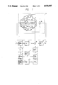
- FIG. 1 is a block diagram of a chrominance signal processing circuit having a circuit for removing crosstalk components in a carrier chrominance signal according to a first embodiment of the present invention
- FIG. 2 is a block diagram of a chrominance signal processing circuit having a circuit for removing crosstalk components in a carrier chrominance signal according to a second embodiment of the invention
- FIG. 3A is a higher-voltage detecting circuit used in the circuit for removing crosstalk components in a carrier chrominance signal
- FIG. 3B is a lower-voltage detecting circuit used in the circuit for removing crosstalk components in a carrier chrominance signal
- FIG. 4 is one example of source images which are to be inputted into the chrominance signal processing circuit of FIG. 1;
- FIGS. 5A, 5B, and 5C are image patterns for describing the operation of the circuit for removing crosstalk components in a carrier chrominance signal
- FIGS. 6A, 6B, 6C, 6D, and 6E are waveforms for describing the operation of the circuit for removing crosstalk components in a carrier chrominance signal
- FIG. 7 is a block diagram of a conventional chrominance signal processing circuit
- FIG. 8A is one example of source images
- FIG. 8B is a reproduced image obtained by supplying the source image of FIG. 8A to the conventional chrominance signal processing circuit.
- the conventional chrominance signal processing circuit generally comprises a main converter 2, a first band-pass filter (BPF) 3, a two-line type chrominance signal comb filter 16, a killer circuit 4, a burst gate 6, a phase comparing circuit 7, a crystal oscillator 8, a loop filter 9, a 160fH voltage
- the two-line type chrominance signal comb filter 16 includes a 1-H delay circuit 14 and a subtractor 15.
- a reproduced frequency down-converted chrominance signal (a) is fed, via an input terminal 1, to the main converter 2.
- the chrominance signal (a) is converted to a carrier chrominance signal (b) having a frequency of 3.58MHz, and then, the carrier chrominance signal (b) is sent to the first BPF 3.
- the first BPF 3 undesired band-width components are removed from the carrier chrominance signal (b).
- An outputted carrier chrominance signal (c) from the first BPF 3 is inputted into the chrominance signal comb filter 16 so as to remove crosstalk components therefrom.
- Such a crosstalk-removed signal (d) is outputted, via the killer circuit 4, from the output terminal 5 as a reproduced chrominance signal (e).
- the crosstalk-removed signal (d) is also fed to the burst gate 6 for producing a burst signal (f).
- the burst signal (f) outputted from the burst gate 6 is inputted into the phase comparing circuit 7.
- a reference signal (g) having a frequency of 3.58MHz is produced by the crystal oscillator 8, and is sent to the phase comparing circuit 7.
- a phase difference signal (h) is produced with the burst signal (f) being compared with the reference signal (g).
- the phase difference signal (h) is inputted into the loop filter 9 to cut undesired, frequency components.
- An outputted signal (i) from the loop filter 9 is sent to the 160fH VCO 10 to be operated as a control voltage thereof, and the 160fH VCO 10 outputs a 160fH signal (j).
- the 160fH signal (j) is frequency-divided and phase-shifted by the 1/4 frequency-dividing and phase-shifting circuit 11 to obtain a signal (k) of frequency 40fH.
- This signal (k) and the reference signal (g) outputted from the crystal oscillator 8 are applied to the sub-converter 12 to produce a signal (l) having a frequency of 4.21MHz.
- This signal (l) of 4.21MHz is sent, via the second BPF 13, to the main converter 2 as a signal (m).
- the 160fH VCO 10 is changed into a 321fH VCO, and the 1/4 frequency-dividing circuit 11 is changed into a 1/8 frequency-dividing circuit.
- the 1-H delay circuit 14 is changed into a 2-H delay circuit.
- the chrominance signal is converted into a signal having a frequency of 4.43MHz, and the crystal oscillator produces a signal having a frequency of 4.43MHz thereby obtaining a 5.06MHz signal from the second BPF.
- a reproduced image has a color-blurring portion (iii) in one line just below the upper red portion (i) as shown in FIG. 8B because there is no vertical-correlation between the upper red portion (i) and the lower colorless portion (ii).
- FIG. 1 shows a block diagram of a chrominance signal processing circuit having a circuit for removing crosstalk components in the NTSC system according to a first embodiment of the present invention.
- the chrominance signal processing circuit of FIG. 1 is substantially the same as that of FIG. 7 except for a chrominance signal comb filter 27, and an adder 28.
- those parts which are the same as those of FIG. 7 are designated by the same numerals and description thereof is omitted.
- the three-line type comb filter 27 includes first and second 1-H delay circuits 20 and 22, an inverter 21, first, second, and third higher-voltage detecting circuits (MAX circuits) 18, 19, and 25, first, second, and third lower-voltage detecting circuits (MIN circuits) 23, 24, and 17, and an adder 26.
- MAX circuits first, second, and third higher-voltage detecting circuits
- MIN circuits first, second, and third lower-voltage detecting circuits
- adder 26 the structure of these MAX circuits 18, 19, and 25 includes transistors Ql and Q2 and a resistor Rl as shown in FIG. 3A
- each of the MIN circuits includes transistors Q3 and Q4 and a resistor R2 as shown in FIG. 3B.
- Carrier chrominance signal (c) from first BPF 3 is fed to the first 1-H delay circuit 20, the first MAX circuit 18, and the first MIN circuit 23 in the three-line type comb filter 27.
- a delayed signal (n) outputted from the first 1-H delay circuit 20 is fed to the inverter 21 and the second 1-H delay circuit 22.
- An inverted signal (p) from the inverter 21 is sent to the first MAX circuit 18, the first MIN circuit 23, the second MAX circuit 19, and the second MIN circuit 24.
- a first higher voltage signal (s) between the carrier chrominance signal (c) and the inverted signal (p) is produced, and then the first higher voltage signal (s) is sent to the third MIN circuit 17.
- a first lower voltage signal (v) between the carrier chrominance signal (c) and the inverted signal (p) is produced, and then the first lower voltage signal (v) is sent to the third MAX circuit 25.
- a delayed signal (o) outputted from the second 1-H delay circuit 22 is also inputted into the second MAX circuit 19 and the second MIN circuit 24.
- the second MAX circuit 19 a second higher voltage signal (t) between the inverted signal (p) and the delayed signal (o) is produced, and then the second higher voltage signal (t) is fed to the third MIN circuit 17.
- the second MIN circuit 24 a second lower voltage signal (w) between the inverted signal (p) and the delayed signal (o) is produced, and then the second lower voltage signal (w) is fed to the third MAX circuit 25.
- a third lower voltage signal (u) between the first higher voltage signal (s) and the second higher voltage signal (t) is produced, and then the third lower voltage signal (u) is supplied to the adder 26.
- a third higher voltage signal (x) between the first lower voltage signal (v) and the second lower voltage signal (w) is produced and then the third higher voltage signal (x) is supplied to the adder 26.
- An added signal (r) from the adder 26 is fed to killer circuit 4.
- the three-line comb filter 27 as a circuit for removing color-blurring and crosstalk component in a carrier chrominance signal will be described hereinbelow. It is assumed that a source image shown in FIG. 4 is applied in the three-line type comb filter 27. This image is formed of an upper colorless portion (A), a middle colored portion (C), and a lower colorless portion (E). A numeral (B) denotes the first line of the middle colored portion (C) and a numeral (D) shows the first line of the lower colorless portion (E).
- signals (c'), (p'), and (o'), which are sequential on a display as horizontal lines, are displayed as shown in FIG. 5A.
- each waveform of the signals (c), (p), (o), (s), (t), (u), (v), (w), (x), and (r) without crosstalk are shown in FIG. 6A.
- the signals (c'), (p'), and (o') are displayed as shown in FIG. 5B.
- each waveform of the signals (c), (p), (o), (s), (t), (u), (v), (w), (x), and (r) are shown in FIG. 6B.
- the signal (r) it can be understood that any chrominance signal is not outputted.
- magenta and green when a hue is reversed between magenta and green as shown in FIG. 5C, i.e. when the signal (o') is magenta and both the signals (p') and (c') are green, each waveform of the signals (c), (p), (o), (s), (t), (u), (v), (w), (x), and (r) is shown in FIG. 6D. It is to be noted that magenta and green can be completely distinguished.
- each waveform of the signals (c), (p), (o), (s), (t), (u), (v), (w), (x), and (r) are shown in FIG. 6E.
- the signal (r) it can be understood that such crosstalk components are substantially removed.
- the signal (r) is outputted therefrom as an average signal between the signal (p) and one closer signal to the signal (p) in the signals (c) and (o), whereby the signal (p) is the main signal therebetween.
- the signal (p) shows a 1-H delayed signal.
- the adder 28 is required for removing the 1-H time duration as one part of a two-line type comb filter.
- the adder 28, the inverter 21, and the 1-H delay circuit 20 form the two-line type comb filter for correcting such a time delay due to the three-line type comb filter 27.
- the signal (c) is added to the signal (p) to produce a signal (q), and the signal (q) is sent to the burst gate 6.
- FIG. 2 shows a block diagram of a chrominance signal processing circuit having a circuit for removing crosstalk components in the NTSC system according to a second embodiment of the present invention.
- the chrominance signal processing circuit of FIG. 2 is substantially the same as that of FIG. 1 except for a chrominance signal comb filter 29.
- those parts which are the same as those of FIG. 7 are designated at the same numerals and description thereof is omitted.
- the three-line type comb filter 29 includes first and second 1-H delay circuits 20 and 22, an inverter 21, first and second 1/4 attenuation circuits 30 and 32, a 1/2 attenuation circuit 31, and an adder 33.
- Carrier chrominance signal (c) from first BPF 3 is fed to the first 1-H delay circuit 20 and the first 1/4 attenuation circuit 30.
- An output signal (n) from the first 1-H delay circuit 20 is sent to the second 1-H delay circuit 22 and the inverter 21.
- an output signal (o) from the second 1-H delay circuit 22 is supplied to the second 1/4 attenuation circuit 32, and an output signal (p) from the inverter 21 is inputted into the 1/2 attenuation circuit 31.
- output signals from the first and second 1/4 attenuation circuits 30 and 32 and the 1/2 attenuation circuit 31 are combined in the adder 33, and then the added signal (r') is sent to the killer circuit 4.
- the signal (p') is produced as a colored signal in which 1/4 of the colored signal is subtracted.
- the signal (o') is produced as a colored signal in which 1/4 of the colored signal is subtracted, and a color component is added to the colorless signal (p') by 1/4. Also in the crosstalk removing circuit of the second embodiment, thus, there is such a great color-blurring removing effect.
- FIGS. 1 and 2 are of the NTSC system, when the above-mentioned present embodiments are applied to that of the PAL system, the following changes are required.
- the 160fH VCO 10 is changed into a 321fH VCO, and the 1/4 frequency-dividing and phase-shifting circuit 11 is changed into a 1/8 frequency-dividing and phase-shifting circuit.
- the first and second 1-H delay, circuits 20 and 22 are respectively changed into 2-H delay circuits.
- the chrominance signal is converted into a signal having a frequency of 4.43MHz, and the crystal oscillator produces a signal having a frequency of 4.43MHz thereby obtaining a 5.06MHz signal from the second BPF 13.
Landscapes
- Engineering & Computer Science (AREA)
- Multimedia (AREA)
- Signal Processing (AREA)
- Processing Of Color Television Signals (AREA)
Applications Claiming Priority (4)
| Application Number | Priority Date | Filing Date | Title |
|---|---|---|---|
| JP62-320872 | 1987-12-18 | ||
| JP32087287A JPH01162090A (ja) | 1987-12-18 | 1987-12-18 | 色信号のクロストーク除去回路 |
| JP63-120576 | 1988-05-19 | ||
| JP12057688A JPH0657069B2 (ja) | 1988-05-19 | 1988-05-19 | カラー映像信号再生装置 |
Related Child Applications (1)
| Application Number | Title | Priority Date | Filing Date |
|---|---|---|---|
| US07/505,182 Division US4969033A (en) | 1987-12-18 | 1990-04-05 | Circuit for removing crosstalk components in a carrier chrominance signal |
Publications (1)
| Publication Number | Publication Date |
|---|---|
| US4930005A true US4930005A (en) | 1990-05-29 |
Family
ID=26458128
Family Applications (2)
| Application Number | Title | Priority Date | Filing Date |
|---|---|---|---|
| US07/285,263 Expired - Lifetime US4930005A (en) | 1987-12-18 | 1988-12-16 | Circuit for removing crosstalk components in a carrier chrominance signal |
| US07/505,182 Expired - Lifetime US4969033A (en) | 1987-12-18 | 1990-04-05 | Circuit for removing crosstalk components in a carrier chrominance signal |
Family Applications After (1)
| Application Number | Title | Priority Date | Filing Date |
|---|---|---|---|
| US07/505,182 Expired - Lifetime US4969033A (en) | 1987-12-18 | 1990-04-05 | Circuit for removing crosstalk components in a carrier chrominance signal |
Country Status (3)
| Country | Link |
|---|---|
| US (2) | US4930005A (de) |
| EP (2) | EP0321312B1 (de) |
| DE (2) | DE3889342T2 (de) |
Cited By (5)
| Publication number | Priority date | Publication date | Assignee | Title |
|---|---|---|---|---|
| US5032902A (en) * | 1988-07-22 | 1991-07-16 | Mitsubishi Denki Kabushiki Kaisha | Playback color processing circuit |
| US5113258A (en) * | 1989-04-10 | 1992-05-12 | Gretag Aktiengesellschaft | Compensation circuit for the correction of image defects of a television image |
| US5153741A (en) * | 1988-08-05 | 1992-10-06 | Victor Company Of Japan, Ltd. | Crosstalk cancelling circuit for playback chrominance signal of VTR |
| US5870153A (en) * | 1997-05-30 | 1999-02-09 | Analog Devices, Inc. | Adaptive comb filter that cancels hugand cross-luminance errors |
| US6023303A (en) * | 1996-02-01 | 2000-02-08 | Sony Corporation | Video signal processing apparatus and method for preventing a signal dropout |
Families Citing this family (11)
| Publication number | Priority date | Publication date | Assignee | Title |
|---|---|---|---|---|
| JPH0251489U (de) * | 1988-10-06 | 1990-04-11 | ||
| DE3939520A1 (de) * | 1989-11-30 | 1991-06-06 | Nokia Unterhaltungselektronik | Schaltung zum rueckgewinnen des chroma-signales |
| JP2840783B2 (ja) * | 1990-03-08 | 1998-12-24 | ソニー株式会社 | ロジカルコムフィルタ |
| US5097347A (en) * | 1990-11-01 | 1992-03-17 | Samsung Electronics Co., Ltd. | Method and apparatus for generating a playback clock from a 2.5 MHz chroma PLL |
| US5267027A (en) * | 1991-04-30 | 1993-11-30 | Sanyo Electric Co., Ltd. | Comb filter-type Y/C separator circuit |
| JP2859526B2 (ja) * | 1992-10-30 | 1999-02-17 | 三星電子株式会社 | 映像信号のノイズ除去回路 |
| JP3290225B2 (ja) * | 1993-01-13 | 2002-06-10 | トウシバビデオプロダクツ プライベート リミテッド | 自動利得調整回路 |
| KR940020852A (ko) * | 1993-02-01 | 1994-09-16 | 이헌조 | 영상신호 처리기기의 휘도 및 칼라 분리장치 |
| JP3323611B2 (ja) * | 1993-06-25 | 2002-09-09 | 株式会社日立製作所 | Vtr用周波数変換装置 |
| US5786871A (en) * | 1996-04-01 | 1998-07-28 | Tektronix, Inc. | Constant luminance corrector |
| FR2748179A1 (fr) * | 1996-04-24 | 1997-10-31 | Thomson Multimedia Sa | Decodeur numerique de signal composite de television couleur, en particulier decodeur numerique multistandard |
Citations (3)
| Publication number | Priority date | Publication date | Assignee | Title |
|---|---|---|---|---|
| EP0218241A2 (de) * | 1985-10-07 | 1987-04-15 | Faroudja Laboratories, Inc. | Zweidimensionaler Kammfilter |
| US4706113A (en) * | 1985-02-18 | 1987-11-10 | Mitsubishi Denki Kabushiki Kaisha | Contour detecting filter device using PAL samples of composite video signals without separation of luminance signals therefrom |
| US4825289A (en) * | 1986-11-11 | 1989-04-25 | Matsushita Electric Industrial Co., Ltd. | Noise reduction apparatus for video signal |
Family Cites Families (3)
| Publication number | Priority date | Publication date | Assignee | Title |
|---|---|---|---|---|
| GB1431378A (en) * | 1972-04-19 | 1976-04-07 | Rca Corp | Colour information translating systems |
| JPH0832067B2 (ja) * | 1984-11-19 | 1996-03-27 | ソニー株式会社 | カラー映像信号の再生装置 |
| JPH07123307B2 (ja) * | 1986-05-20 | 1995-12-25 | ソニー株式会社 | Y/c分離回路 |
-
1988
- 1988-12-16 US US07/285,263 patent/US4930005A/en not_active Expired - Lifetime
- 1988-12-19 EP EP88312021A patent/EP0321312B1/de not_active Expired
- 1988-12-19 DE DE3889342T patent/DE3889342T2/de not_active Expired - Lifetime
- 1988-12-19 DE DE8888312021T patent/DE3863634D1/de not_active Expired - Lifetime
- 1988-12-19 EP EP90202673A patent/EP0411725B1/de not_active Expired - Lifetime
-
1990
- 1990-04-05 US US07/505,182 patent/US4969033A/en not_active Expired - Lifetime
Patent Citations (3)
| Publication number | Priority date | Publication date | Assignee | Title |
|---|---|---|---|---|
| US4706113A (en) * | 1985-02-18 | 1987-11-10 | Mitsubishi Denki Kabushiki Kaisha | Contour detecting filter device using PAL samples of composite video signals without separation of luminance signals therefrom |
| EP0218241A2 (de) * | 1985-10-07 | 1987-04-15 | Faroudja Laboratories, Inc. | Zweidimensionaler Kammfilter |
| US4825289A (en) * | 1986-11-11 | 1989-04-25 | Matsushita Electric Industrial Co., Ltd. | Noise reduction apparatus for video signal |
Non-Patent Citations (4)
| Title |
|---|
| IEEE Transactions on Consumer Electronics, vol. CE 31, No. 3, Aug. 1985, pp. 240 253, IEEE, New York, U.S.; T. Okada et al.: Flicker Free Non Interlaced Receiving System for Standard Color TV Signals . * |
| IEEE Transactions on Consumer Electronics, vol. CE-31, No. 3, Aug. 1985, pp. 240-253, IEEE, New York, U.S.; T. Okada et al.: "Flicker-Free Non Interlaced Receiving System for Standard Color TV Signals". |
| Wireless World, vol. 89, Dec. 1975, pp. 74 79, Olchester, GB; D. Read: Improving Color Television Decoding . * |
| Wireless World, vol. 89, Dec. 1975, pp. 74-79, Olchester, GB; D. Read: "Improving Color Television Decoding". |
Cited By (5)
| Publication number | Priority date | Publication date | Assignee | Title |
|---|---|---|---|---|
| US5032902A (en) * | 1988-07-22 | 1991-07-16 | Mitsubishi Denki Kabushiki Kaisha | Playback color processing circuit |
| US5153741A (en) * | 1988-08-05 | 1992-10-06 | Victor Company Of Japan, Ltd. | Crosstalk cancelling circuit for playback chrominance signal of VTR |
| US5113258A (en) * | 1989-04-10 | 1992-05-12 | Gretag Aktiengesellschaft | Compensation circuit for the correction of image defects of a television image |
| US6023303A (en) * | 1996-02-01 | 2000-02-08 | Sony Corporation | Video signal processing apparatus and method for preventing a signal dropout |
| US5870153A (en) * | 1997-05-30 | 1999-02-09 | Analog Devices, Inc. | Adaptive comb filter that cancels hugand cross-luminance errors |
Also Published As
| Publication number | Publication date |
|---|---|
| EP0411725A2 (de) | 1991-02-06 |
| EP0321312B1 (de) | 1991-07-10 |
| US4969033A (en) | 1990-11-06 |
| DE3863634D1 (de) | 1991-08-14 |
| DE3889342T2 (de) | 1994-09-01 |
| DE3889342D1 (de) | 1994-06-01 |
| EP0321312A1 (de) | 1989-06-21 |
| EP0411725B1 (de) | 1994-04-27 |
| EP0411725A3 (en) | 1991-05-02 |
Similar Documents
| Publication | Publication Date | Title |
|---|---|---|
| US4930005A (en) | Circuit for removing crosstalk components in a carrier chrominance signal | |
| JPS62242485A (ja) | 映像信号記録または再生システム | |
| JP2655672B2 (ja) | ビデオレコーダー用の篩形フィルタ | |
| JPS6231293A (ja) | 映像信号記録再生装置 | |
| US5802238A (en) | Circuit arrangement for processing a color signal at a carrier frequency higher than a carrier frequency at which the color signal had been recorded | |
| JP2524521B2 (ja) | 磁気記録再生装置 | |
| JP4050381B2 (ja) | 色信号処理用回路装置 | |
| US5500740A (en) | Video signal processing with common delay line for luminance interpolation and color conversion | |
| JP2936723B2 (ja) | 色信号再生装置 | |
| JP3110196B2 (ja) | クシ型フィルタ自動調整回路 | |
| JPS62135095A (ja) | 映像信号記録再生装置の輝度信号処理装置 | |
| JPH0657069B2 (ja) | カラー映像信号再生装置 | |
| JPS63292794A (ja) | ディジタルy/c分離装置 | |
| KR960008678Y1 (ko) | 브이씨알(vcr)의 휘도 칼라 분리장치 | |
| JP3123063B2 (ja) | 記録・再生装置 | |
| JPH0326088A (ja) | 磁気記録再生装置 | |
| JPH067684B2 (ja) | 映像信号処理装置 | |
| JPH04101585A (ja) | 記録装置 | |
| JPH02257788A (ja) | 磁気記録再生装置 | |
| JPS62235894A (ja) | Vtrのカラ−信号処理回路 | |
| JPS62296693A (ja) | 映像信号処理装置 | |
| JPH01165292A (ja) | 色信号処理装置 | |
| JPS586437B2 (ja) | キロクサイセイホウシキ | |
| JPS60132493A (ja) | 搬送色信号の処理装置 | |
| JPH06105334A (ja) | フィールド変換装置 |
Legal Events
| Date | Code | Title | Description |
|---|---|---|---|
| AS | Assignment |
Owner name: VICTOR COMPANY OF JAPAN, LTD., JAPAN Free format text: ASSIGNMENT OF ASSIGNORS INTEREST.;ASSIGNORS:YAMADA, HIROSHI;NAKANO, RYO;MATSUO, YASUTOSHI;AND OTHERS;REEL/FRAME:005009/0307 Effective date: 19881214 |
|
| STCF | Information on status: patent grant |
Free format text: PATENTED CASE |
|
| FEPP | Fee payment procedure |
Free format text: PAYOR NUMBER ASSIGNED (ORIGINAL EVENT CODE: ASPN); ENTITY STATUS OF PATENT OWNER: LARGE ENTITY |
|
| FPAY | Fee payment |
Year of fee payment: 4 |
|
| FPAY | Fee payment |
Year of fee payment: 8 |
|
| FPAY | Fee payment |
Year of fee payment: 12 |