US4996448A - Low power peak detector/buffer with fast charge-up time - Google Patents
Low power peak detector/buffer with fast charge-up time Download PDFInfo
- Publication number
- US4996448A US4996448A US07/442,272 US44227289A US4996448A US 4996448 A US4996448 A US 4996448A US 44227289 A US44227289 A US 44227289A US 4996448 A US4996448 A US 4996448A
- Authority
- US
- United States
- Prior art keywords
- coupled
- transistor
- output
- emitter
- collector
- Prior art date
- Legal status (The legal status is an assumption and is not a legal conclusion. Google has not performed a legal analysis and makes no representation as to the accuracy of the status listed.)
- Expired - Lifetime
Links
Images
Classifications
-
- G—PHYSICS
- G01—MEASURING; TESTING
- G01R—MEASURING ELECTRIC VARIABLES; MEASURING MAGNETIC VARIABLES
- G01R19/00—Arrangements for measuring currents or voltages or for indicating presence or sign thereof
- G01R19/04—Measuring peak values or amplitude or envelope of AC or of pulses
-
- H—ELECTRICITY
- H03—ELECTRONIC CIRCUITRY
- H03K—PULSE TECHNIQUE
- H03K5/00—Manipulating of pulses not covered by one of the other main groups of this subclass
- H03K5/153—Arrangements in which a pulse is delivered at the instant when a predetermined characteristic of an input signal is present or at a fixed time interval after this instant
- H03K5/1532—Peak detectors
Definitions
- the present invention relates to peak detectors and, more particularly, to a circuit and method for detecting the most positive peak level of a signal.
- Peak detectors are usually used to track the most positive peak voltage level of a signal.
- the desired output of a peak detector typically represents the most positive peak voltage level of its input signal.
- prior art peak detectors are designed to detect the most negative peak voltage level of an input signal thereby constituting a need for inverters to implement a peak detector that detects positive peak voltage levels whereby the use of inverters creates additional offset errors.
- the basic theory of a peak detector is to compare the input voltage level to the output voltage level to determine if the input signal has reached a new peak voltage level. If indeed the input signal has reached a new peak, the peak detector will respond in a manner to increase the voltage level of the output signal until it has attained the same voltage of the peak input signal.
- a common technique use by most peak detectors is a charge up a capacitor wherein the voltage across the capacitor represents the peak voltage level of the input signal so that when the input voltage falls below the output voltage, the capacitor maintains the peak input voltage level at the output of the peak detector.
- Peak detectors can be evaluated with respect to attack time and power dissipation.
- Attack time is defined as the finite time required by a peak detector to adjust its output voltage level in accordance to a new peak voltage level occurring in the input signal. Attack time is dependent upon two main factors: the ability to prevent the switching transistors from entering saturation wherein the switching transistors compare the input voltage level to the output voltage level, and the speed at which the capacitor in the peak detector is charged up. Most, if not all, peak detectors have been unable to prevent the switching transistors from entering the saturation region thereby increasing the time required for the peak detector to respond to a new peak voltage level since a finite time is required to allow a saturated transistor to become active.
- the speed at which the capacitor in the peak detector can be charged up is particularly important for rapidly changing input signals.
- a capacitor must charge up to the full peak voltage of the input signal level by the time the peak input level disappears or the true peak level will not have been recognized.
- the charge up time of a capacitor is related to the current through the capacitor by the following equation:
- t cu is the charge up time of the capacitor C
- V p is the peak voltage that we wish to obtain at the output
- I is the current through the capacitor C.
- a quick charge up time (t cu ) requires a large current (I) thereby increasing the power dissipation of the peak detector.
- I current
- peak detectors have satiated their required charge up time by simply increasing the power dissipation; however, if power dissipation is critical, compensation must result in an increased attack time.
- a peak detector that detects the positive peak voltage level of an input signal and having a quick attack time while minimizing power dissipation.
- Another object of the present invention is to decrease the attack time of the peak detector circuit while minimizing power dissipation.
- Yet another object of the present invention is to minimize the inaccuracies and offsets of positive peak voltage level detectors by abating the need for inverters.
- a circuit having an output signal at an output which represents the most positive peak voltage level of an input signal applied at an input, comprising comparator circuit for comparing the voltage level of the input signal to the voltage level of the output signal for providing an output current at an output whenever the voltage level of the input signal exceeds that of the output signal; an amplification circuit responsive to the output current of the comparator circuit for amplifying the output current to charge a capacitive circuit to a voltage that is substantially equal to the most positive peak voltage level of the input signal; a buffer circuit to transform the voltage across the capacitor circuit to the output which further includes a clamping circuit for clamping the output of the comparator circuit to substantially the value of the output signal whenever the applied input signal is less than the output signal.
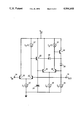
- FIGURE is a schematic diagram illustrating the preferred embodiment of the present invention.
- comparator circuit which includes a pair of differentially connected transistors 10 and 12 having their emitters returned to ground reference by an independent current source 13, and their bases coupled to input terminal 14 and output terminal 16, respectively.
- the collector of transistor 10 is coupled to operating potential V CC while the collector of transistor 12 is coupled to operating potential V CC by independent current source 17 which is selected to supply precisely one half the current of independent current source 13 thereby minimizing any offset error.
- transistor 22 having a collector coupled to operating potential V CC a base coupled to the collector of transistor 12 of the comparator circuit, and an emitter coupled to ground reference by capacitive means comprising capacitor 24.
- the present invention further comprises buffer circuit comprising a pair of differentially connected transistors 26 and 28 having their emitters coupled to ground reference by independent current source 30, and their bases coupled to the emitter of transistor 22 of the amplification circuit and to output terminal 16, respectively.
- the collector of transistor 26 is coupled to operating potential V CC while the collector of transistor 28 is coupled to operating potential V CC by independent current source 32, and to the base of transistor 34 which has a collector coupled to operating potential V CC .
- independent current source 32 is selected to supply precisely one half the current of independent current source 30 thereby minimizing any offset error.
- the emitter of transistor 34 is coupled to output terminal 16 by diode 20 and to the collector of transistor 12 of the comparator circuit by diode 18. It is understood that diodes 18 and 20 may be similarly formed by transistors having their bases and collectors shorted together.
- output terminal 16 is coupled to ground reference by independent current source 36 for biasing transistor 34 and diode 20.
- the present invention functions to produce an output signal that represents the positive peak voltage level of its input.
- all the current of independent current source 13 of value I T flows through transistor 10, while transistor 12 is off. Since transistor 12 is off, all the current of independent current source 17 of value I T /2 flows into the base of transistor 22 thereby charging up capacitor 24 with an amplified current of I T /2 multiplied by the beta or transistor 22.
- This allows both current sources, 17 and 13, to be very small and still supply significant current to charge up capacitor 24. Therefore, when comparing the charge time of the present invention to other peak detectors the present invention requires much less power to achieve the same charge up time thereby conserving an appreciable amount of power consumption.
- the present invention requires no inverters since it is designed to directly detect the most positive voltage level of the input signal thereby eliminating any offset errors due to the inverters.
- the differential amplifier pair comprised of transistors 26 and 28 function as a buffer circuit to transform the voltage across capacitor 24 to output terminal 16 wherein the voltage across capacitor 24 denotes the positive peak voltage level at input terminal 14.
- the present invention functions to preserve the voltage across capacitor 24 at output terminal 16 via the buffer circuit which maintains the voltage at the base of transistor 26 equal to the voltage at the base of transistor 28, and to prevent transistor 12 from saturating.
- all the current of independent current source 13 of value I T flow through transistor 12 while transistor 10 is off.
- One half of the required I T current is obtained from independent current source 17, but if the other hal of I T is not provided from another source, transistor 12 will saturate.
- clamping means comprising diodes 18 and 209 provide a method to source the additional current of I T /2 and prevent transistor 12 from ever saturating.
- the needed current of value I T /2 is provided from the emitter of transistor 34, passed through diode 18 and injected at the collector of transistor 12. Furthermore, transistor 12 will never enter saturation since diodes 18 and 20 form a clamp to prevent the voltage at the collector of transistor 12 from falling below the voltage at the base of transistor 12. It is important to realize that the collector of transistor 12 is clamped to voltage V OUT while the base of transistor 26 is also maintained at V OUT by capacitor 24 which means that the base and emitter of transistor 22 is maintained at a voltage substantially equal to V OUT and, thus, transistor 22 is OFF.
Landscapes
- Physics & Mathematics (AREA)
- Nonlinear Science (AREA)
- Engineering & Computer Science (AREA)
- Power Engineering (AREA)
- General Physics & Mathematics (AREA)
- Measurement Of Current Or Voltage (AREA)
Priority Applications (2)
| Application Number | Priority Date | Filing Date | Title |
|---|---|---|---|
| US07/442,272 US4996448A (en) | 1989-11-27 | 1989-11-27 | Low power peak detector/buffer with fast charge-up time |
| JP31820090A JP3203363B2 (ja) | 1989-11-27 | 1990-11-26 | ピーク検出器 |
Applications Claiming Priority (1)
| Application Number | Priority Date | Filing Date | Title |
|---|---|---|---|
| US07/442,272 US4996448A (en) | 1989-11-27 | 1989-11-27 | Low power peak detector/buffer with fast charge-up time |
Publications (1)
| Publication Number | Publication Date |
|---|---|
| US4996448A true US4996448A (en) | 1991-02-26 |
Family
ID=23756187
Family Applications (1)
| Application Number | Title | Priority Date | Filing Date |
|---|---|---|---|
| US07/442,272 Expired - Lifetime US4996448A (en) | 1989-11-27 | 1989-11-27 | Low power peak detector/buffer with fast charge-up time |
Country Status (2)
| Country | Link |
|---|---|
| US (1) | US4996448A (ja) |
| JP (1) | JP3203363B2 (ja) |
Cited By (9)
| Publication number | Priority date | Publication date | Assignee | Title |
|---|---|---|---|---|
| US5068552A (en) * | 1990-09-10 | 1991-11-26 | Kabushiki Kaisha Toshiba | Voltage follower circuit having improved dynamic range |
| US5120995A (en) * | 1991-05-29 | 1992-06-09 | Motorola, Inc. | Switched peak detector |
| US5345337A (en) * | 1993-01-28 | 1994-09-06 | Lockheed Missiles & Space Company, Inc. | Viscous supercooled liquid lens elements having abnormal dispersion |
| USRE34771E (en) * | 1989-09-11 | 1994-11-01 | Kabushiki Kaisha Toshiba | Voltage follower circuit having improved dynamic range |
| US5362992A (en) * | 1992-06-01 | 1994-11-08 | National Semiconductor Corporation | Electronic control of peak detector response time |
| US6051998A (en) * | 1998-04-22 | 2000-04-18 | Mitsubishi Semiconductor America, Inc. | Offset-compensated peak detector with output buffering |
| US6054874A (en) * | 1997-07-02 | 2000-04-25 | Cypress Semiconductor Corp. | Output driver circuit with switched current source |
| US6084439A (en) * | 1997-07-02 | 2000-07-04 | Cypress Semiconductor Corp. | Peak detector circuit with extended input voltage range |
| US6535027B1 (en) * | 2000-05-05 | 2003-03-18 | Westell, Inc. | Low power peak detector |
Families Citing this family (3)
| Publication number | Priority date | Publication date | Assignee | Title |
|---|---|---|---|---|
| JP2638297B2 (ja) * | 1989-12-25 | 1997-08-06 | 日本電気株式会社 | ピークレベル検出回路 |
| DE69227743T2 (de) | 1991-09-18 | 1999-04-22 | Fujitsu Ltd., Kawasaki, Kanagawa | Integrierte Halbleiterschaltung mit Abtastpfad |
| JP2002368591A (ja) * | 2001-06-12 | 2002-12-20 | Sony Corp | ピークホールド回路 |
Citations (5)
| Publication number | Priority date | Publication date | Assignee | Title |
|---|---|---|---|---|
| US3643110A (en) * | 1970-11-30 | 1972-02-15 | Motorola Inc | Sample and hold circuit |
| US4533844A (en) * | 1982-02-26 | 1985-08-06 | Motorola, Inc. | Peak storage amplifier |
| US4603299A (en) * | 1982-07-26 | 1986-07-29 | Memory Technology, Inc. | Constant duty cycle peak detector |
| US4720643A (en) * | 1981-10-13 | 1988-01-19 | American Telephone And Telegraph Company, At&T Bell Laboratories | Peak catcher circuit |
| JPS63131072A (ja) * | 1986-11-20 | 1988-06-03 | Mitsubishi Electric Corp | ピ−ク検出回路 |
-
1989
- 1989-11-27 US US07/442,272 patent/US4996448A/en not_active Expired - Lifetime
-
1990
- 1990-11-26 JP JP31820090A patent/JP3203363B2/ja not_active Expired - Lifetime
Patent Citations (5)
| Publication number | Priority date | Publication date | Assignee | Title |
|---|---|---|---|---|
| US3643110A (en) * | 1970-11-30 | 1972-02-15 | Motorola Inc | Sample and hold circuit |
| US4720643A (en) * | 1981-10-13 | 1988-01-19 | American Telephone And Telegraph Company, At&T Bell Laboratories | Peak catcher circuit |
| US4533844A (en) * | 1982-02-26 | 1985-08-06 | Motorola, Inc. | Peak storage amplifier |
| US4603299A (en) * | 1982-07-26 | 1986-07-29 | Memory Technology, Inc. | Constant duty cycle peak detector |
| JPS63131072A (ja) * | 1986-11-20 | 1988-06-03 | Mitsubishi Electric Corp | ピ−ク検出回路 |
Non-Patent Citations (2)
| Title |
|---|
| N. D. Nguyen, "Simple Peak Detector", IBM Technical Disclosure Bulletin, vol. 27, No. 2, Jul. 1984, pp. 1368-1369. |
| N. D. Nguyen, Simple Peak Detector , IBM Technical Disclosure Bulletin, vol. 27, No. 2, Jul. 1984, pp. 1368 1369. * |
Cited By (9)
| Publication number | Priority date | Publication date | Assignee | Title |
|---|---|---|---|---|
| USRE34771E (en) * | 1989-09-11 | 1994-11-01 | Kabushiki Kaisha Toshiba | Voltage follower circuit having improved dynamic range |
| US5068552A (en) * | 1990-09-10 | 1991-11-26 | Kabushiki Kaisha Toshiba | Voltage follower circuit having improved dynamic range |
| US5120995A (en) * | 1991-05-29 | 1992-06-09 | Motorola, Inc. | Switched peak detector |
| US5362992A (en) * | 1992-06-01 | 1994-11-08 | National Semiconductor Corporation | Electronic control of peak detector response time |
| US5345337A (en) * | 1993-01-28 | 1994-09-06 | Lockheed Missiles & Space Company, Inc. | Viscous supercooled liquid lens elements having abnormal dispersion |
| US6054874A (en) * | 1997-07-02 | 2000-04-25 | Cypress Semiconductor Corp. | Output driver circuit with switched current source |
| US6084439A (en) * | 1997-07-02 | 2000-07-04 | Cypress Semiconductor Corp. | Peak detector circuit with extended input voltage range |
| US6051998A (en) * | 1998-04-22 | 2000-04-18 | Mitsubishi Semiconductor America, Inc. | Offset-compensated peak detector with output buffering |
| US6535027B1 (en) * | 2000-05-05 | 2003-03-18 | Westell, Inc. | Low power peak detector |
Also Published As
| Publication number | Publication date |
|---|---|
| JP3203363B2 (ja) | 2001-08-27 |
| JPH03181868A (ja) | 1991-08-07 |
Similar Documents
| Publication | Publication Date | Title |
|---|---|---|
| GB2259782A (en) | Detecting RF signals | |
| US5132609A (en) | Circuit for measuring the level of an electrical signal and including offset correction means, and application thereof to amplifiers having automatic gain control | |
| JP3337079B2 (ja) | 電源回路 | |
| US3959733A (en) | Differential amplifier | |
| GB1367660A (en) | Circuit for generating a difference current value between a pair of current mode input signals | |
| JP3203363B2 (ja) | ピーク検出器 | |
| US4247949A (en) | Signal strength detecting circuit | |
| US3968453A (en) | Gain control circuit | |
| US4368395A (en) | Differential linear to digital translator | |
| US4460876A (en) | Low consumption, wide-band linear amplifier operating in sliding class A | |
| FI79436C (fi) | Bildvisningsanordning. | |
| US4405902A (en) | Push-pull output stage | |
| CA1301862C (en) | Logarithmic amplification circuit for obtaining output voltage corresponding to difference between logarithmically amplified values of two input currents | |
| JPH09120317A (ja) | 高精度定電流源回路 | |
| US4554468A (en) | Latching comparator with hysteresis | |
| US2926308A (en) | Transistor biasing circuit | |
| JP2680753B2 (ja) | バッファアンプ | |
| US4990863A (en) | Amplifier output stage | |
| RU2007846C1 (ru) | Усилитель напряжения с компенсацией напряжения смещения | |
| SU764099A1 (ru) | Дифференциальный усилитель | |
| KR100271590B1 (ko) | 차동 증폭 장치 | |
| JPH0348683B2 (ja) | ||
| JPH10503347A (ja) | 動作速度及び精度を改善した帰還増幅器 | |
| GB2178259A (en) | Amplifier with controllable amplification | |
| JPS6246326Y2 (ja) |
Legal Events
| Date | Code | Title | Description |
|---|---|---|---|
| AS | Assignment |
Owner name: MOTOROLA, INC., SCHAUMBURG, ILLINOIS, A CORP. OF D Free format text: ASSIGNMENT OF ASSIGNORS INTEREST.;ASSIGNOR:ABDI, BEHROOZ L.;REEL/FRAME:005188/0954 Effective date: 19891121 |
|
| STCF | Information on status: patent grant |
Free format text: PATENTED CASE |
|
| FPAY | Fee payment |
Year of fee payment: 4 |
|
| FPAY | Fee payment |
Year of fee payment: 8 |
|
| FPAY | Fee payment |
Year of fee payment: 12 |
|
| AS | Assignment |
Owner name: FREESCALE SEMICONDUCTOR, INC., TEXAS Free format text: ASSIGNMENT OF ASSIGNORS INTEREST;ASSIGNOR:MOTOROLA, INC.;REEL/FRAME:015698/0657 Effective date: 20040404 Owner name: FREESCALE SEMICONDUCTOR, INC.,TEXAS Free format text: ASSIGNMENT OF ASSIGNORS INTEREST;ASSIGNOR:MOTOROLA, INC.;REEL/FRAME:015698/0657 Effective date: 20040404 |
|
| AS | Assignment |
Owner name: CITIBANK, N.A. AS COLLATERAL AGENT, NEW YORK Free format text: SECURITY AGREEMENT;ASSIGNORS:FREESCALE SEMICONDUCTOR, INC.;FREESCALE ACQUISITION CORPORATION;FREESCALE ACQUISITION HOLDINGS CORP.;AND OTHERS;REEL/FRAME:018855/0129 Effective date: 20061201 Owner name: CITIBANK, N.A. AS COLLATERAL AGENT,NEW YORK Free format text: SECURITY AGREEMENT;ASSIGNORS:FREESCALE SEMICONDUCTOR, INC.;FREESCALE ACQUISITION CORPORATION;FREESCALE ACQUISITION HOLDINGS CORP.;AND OTHERS;REEL/FRAME:018855/0129 Effective date: 20061201 |
|
| AS | Assignment |
Owner name: FREESCALE SEMICONDUCTOR, INC., TEXAS Free format text: PATENT RELEASE;ASSIGNOR:CITIBANK, N.A., AS COLLATERAL AGENT;REEL/FRAME:037354/0225 Effective date: 20151207 |