US5066945A - Driving apparatus for an electrode matrix suitable for a liquid crystal panel - Google Patents
Driving apparatus for an electrode matrix suitable for a liquid crystal panel Download PDFInfo
- Publication number
- US5066945A US5066945A US07/262,576 US26257688A US5066945A US 5066945 A US5066945 A US 5066945A US 26257688 A US26257688 A US 26257688A US 5066945 A US5066945 A US 5066945A
- Authority
- US
- United States
- Prior art keywords
- voltage
- voltages
- generating
- liquid crystal
- fixed
- Prior art date
- Legal status (The legal status is an assumption and is not a legal conclusion. Google has not performed a legal analysis and makes no representation as to the accuracy of the status listed.)
- Expired - Lifetime
Links
- 239000011159 matrix material Substances 0.000 title claims abstract description 15
- 239000004973 liquid crystal related substance Substances 0.000 title claims description 27
- 238000007792 addition Methods 0.000 claims 6
- 239000000758 substrate Substances 0.000 claims 6
- 239000004990 Smectic liquid crystal Substances 0.000 claims 4
- 239000005262 ferroelectric liquid crystals (FLCs) Substances 0.000 description 14
- 238000010586 diagram Methods 0.000 description 12
- 238000000034 method Methods 0.000 description 6
- 238000005070 sampling Methods 0.000 description 4
- 230000007423 decrease Effects 0.000 description 2
- 230000033228 biological regulation Effects 0.000 description 1
- 239000003990 capacitor Substances 0.000 description 1
- 230000000717 retained effect Effects 0.000 description 1
Images


Classifications
-
- G—PHYSICS
- G09—EDUCATION; CRYPTOGRAPHY; DISPLAY; ADVERTISING; SEALS
- G09G—ARRANGEMENTS OR CIRCUITS FOR CONTROL OF INDICATING DEVICES USING STATIC MEANS TO PRESENT VARIABLE INFORMATION
- G09G3/00—Control arrangements or circuits, of interest only in connection with visual indicators other than cathode-ray tubes
- G09G3/20—Control arrangements or circuits, of interest only in connection with visual indicators other than cathode-ray tubes for presentation of an assembly of a number of characters, e.g. a page, by composing the assembly by combination of individual elements arranged in a matrix no fixed position being assigned to or needed to be assigned to the individual characters or partial characters
- G09G3/34—Control arrangements or circuits, of interest only in connection with visual indicators other than cathode-ray tubes for presentation of an assembly of a number of characters, e.g. a page, by composing the assembly by combination of individual elements arranged in a matrix no fixed position being assigned to or needed to be assigned to the individual characters or partial characters by control of light from an independent source
- G09G3/36—Control arrangements or circuits, of interest only in connection with visual indicators other than cathode-ray tubes for presentation of an assembly of a number of characters, e.g. a page, by composing the assembly by combination of individual elements arranged in a matrix no fixed position being assigned to or needed to be assigned to the individual characters or partial characters by control of light from an independent source using liquid crystals
- G09G3/3611—Control of matrices with row and column drivers
- G09G3/3622—Control of matrices with row and column drivers using a passive matrix
- G09G3/3629—Control of matrices with row and column drivers using a passive matrix using liquid crystals having memory effects, e.g. ferroelectric liquid crystals
-
- G—PHYSICS
- G09—EDUCATION; CRYPTOGRAPHY; DISPLAY; ADVERTISING; SEALS
- G09G—ARRANGEMENTS OR CIRCUITS FOR CONTROL OF INDICATING DEVICES USING STATIC MEANS TO PRESENT VARIABLE INFORMATION
- G09G3/00—Control arrangements or circuits, of interest only in connection with visual indicators other than cathode-ray tubes
- G09G3/20—Control arrangements or circuits, of interest only in connection with visual indicators other than cathode-ray tubes for presentation of an assembly of a number of characters, e.g. a page, by composing the assembly by combination of individual elements arranged in a matrix no fixed position being assigned to or needed to be assigned to the individual characters or partial characters
- G09G3/34—Control arrangements or circuits, of interest only in connection with visual indicators other than cathode-ray tubes for presentation of an assembly of a number of characters, e.g. a page, by composing the assembly by combination of individual elements arranged in a matrix no fixed position being assigned to or needed to be assigned to the individual characters or partial characters by control of light from an independent source
- G09G3/36—Control arrangements or circuits, of interest only in connection with visual indicators other than cathode-ray tubes for presentation of an assembly of a number of characters, e.g. a page, by composing the assembly by combination of individual elements arranged in a matrix no fixed position being assigned to or needed to be assigned to the individual characters or partial characters by control of light from an independent source using liquid crystals
-
- G—PHYSICS
- G09—EDUCATION; CRYPTOGRAPHY; DISPLAY; ADVERTISING; SEALS
- G09G—ARRANGEMENTS OR CIRCUITS FOR CONTROL OF INDICATING DEVICES USING STATIC MEANS TO PRESENT VARIABLE INFORMATION
- G09G3/00—Control arrangements or circuits, of interest only in connection with visual indicators other than cathode-ray tubes
- G09G3/20—Control arrangements or circuits, of interest only in connection with visual indicators other than cathode-ray tubes for presentation of an assembly of a number of characters, e.g. a page, by composing the assembly by combination of individual elements arranged in a matrix no fixed position being assigned to or needed to be assigned to the individual characters or partial characters
- G09G3/34—Control arrangements or circuits, of interest only in connection with visual indicators other than cathode-ray tubes for presentation of an assembly of a number of characters, e.g. a page, by composing the assembly by combination of individual elements arranged in a matrix no fixed position being assigned to or needed to be assigned to the individual characters or partial characters by control of light from an independent source
- G09G3/36—Control arrangements or circuits, of interest only in connection with visual indicators other than cathode-ray tubes for presentation of an assembly of a number of characters, e.g. a page, by composing the assembly by combination of individual elements arranged in a matrix no fixed position being assigned to or needed to be assigned to the individual characters or partial characters by control of light from an independent source using liquid crystals
- G09G3/3611—Control of matrices with row and column drivers
- G09G3/3696—Generation of voltages supplied to electrode drivers
-
- G—PHYSICS
- G09—EDUCATION; CRYPTOGRAPHY; DISPLAY; ADVERTISING; SEALS
- G09G—ARRANGEMENTS OR CIRCUITS FOR CONTROL OF INDICATING DEVICES USING STATIC MEANS TO PRESENT VARIABLE INFORMATION
- G09G2320/00—Control of display operating conditions
- G09G2320/04—Maintaining the quality of display appearance
- G09G2320/041—Temperature compensation
Definitions
- the present invention relates to a driving apparatus, particularly a drive voltage generating apparatus for a ferroelectric liquid crystal panel.
- a scanning electrode driver is supplied with the voltages V 11 , V 12 , V 15 and V 16
- a data electrode driver is supplied with the voltages V 11 , V 12 , V 13 and V 14 .
- the scanning electrode driver supplies a scanning selection pulse with a voltage V 11 and a scanning non-selection pulse with a voltage V 15 to scanning electrodes in an odd-numbered frame operation, and a scanning selection pulse with a voltage V.sub. 12 of an opposite polarity to the voltages V 11 and V 15 , with respect to the voltage level V SS as the standard, and a scanning non-selection pulse with a voltage V 16 to the scanning electrodes in even-numbered frame operations.
- the data electrode driver supplies a data selection pulse voltage V 12 and a data non-selection pulse voltage V 13 to the data electrodes in synchronism with the scanning selection pulse V 11 in the odd frame, and a data selection pulse voltage V 11 of an opposite polarity to the voltages V 12 and V 13 , with respect to the voltage level V SS , and a data non-selection pulse voltage V 14 to the data electrodes in synchronism with the scanning selection pulse voltage V 12 in the even frame.
- the system shown in FIG. 9 further includes a trimmer Rv for changing the application voltage which may be used for adjusting a contrast of the display panel. More specifically, by adjusting the application voltage trimmer Rv, the voltage levels V 12 -V 16 can be varied with the voltage level V 11 at the maximum so that the voltages applied to the liquid crystal panel can be varied.
- the scanning electrode driver and data electrode driver are supplied with supply voltages (V DD -V SS ), and the voltage applied to a liquid crystal pixel at the time of selection becomes V 11 -V 12 , so that the maximum voltage applied to a liquid crystal pixel depends on the withstand voltage of the drive unit.
- the amplitude of the scanning selection signal voltage is (V 11 -V 12 ), and the amplitude of the data selection or non-selection signal voltage is (V 13 -V 14 ), that is (V 11 -V 12 )/2.
- V 11 is fixed as the highest voltage and division voltages V 13 , Vc, V 14 and V 12 are generated as in the above-mentioned drive of a TN-type liquid crystal panel, and the division voltages are used for driving a ferroelectric liquid crystal panel, the maximum voltage applicable to a pixel is (V 11 -V 14 ).
- V 11 22 volts
- V 13 16.5 volts
- Vc 11 volts
- V 14 5.5 volts
- V 12 0 volt
- a driving unit of the same withstand voltage provides a smaller maximum voltage applicable to a pixel for a ferroelectric liquid crystal panel because of the difference between the driving methods.
- FIG. 11 illustrates a relationship between the drive voltage and the application time
- FIG. 12 illustrates a relationship between the temperature and the drive voltage. More specifically, in FIG. 11, the abscissa represents the voltage V (voltage applied to a pixel shown in FIG. 10), the ordinate represents the pulse duration ⁇ T (pulse duration shown in FIG. 10 required for inverting the orientation at a pixel), and the dependence of the pulse duration ⁇ T on the charge in drive voltage V is illustrated. As shown in the figure, the pulse duration can be shortened as the drive voltage becomes higher.
- the abscissa represents the temperature (Temp.)
- the ordinate represents the drive voltage (log V) in a logarithmic scale
- the dependence of the threshold voltage Vth on the temperature change is shown at a fixed pulse duration ⁇ T.
- a lower temperature requires a higher driving voltage. It is understood from FIGS. 11 and 12 that an increased voltage applicable to a pixel allows for a higher switching speed and a wider dynamic or operable temperature range.
- designing of a drive unit (IC) having an increased withstand voltage for providing a required drive voltage results in a slow operation speed of a logic circuit in the data electrode driver.
- Such a slow operation speed results in a decrease in the amount of image data transferable in a fixed period (horizontal scanning period), so that it becomes difficult to realize a large size and highly fine liquid crystal display with a large number of pixels.
- Another object of the present invention is to provide a driving apparatus suitable for realization of an appropriate temperature compensation.
- a driving apparatus comprising:
- a driving unit including a scanning electrode driver and a data electrode driver for driving an electrode matrix formed of scanning electrodes and data electrodes, and
- a drive voltage generating unit including a first means for generating a fixed voltage, a second means for generating a source voltage for providing drive voltages for driving the electrode matrix, and a third means for generating a first voltage equal to a subtraction of the fixed voltage from the source voltage and a second voltage equal to a subtraction of the source voltage from the fixed voltage.
- the driving apparatus further provided with an appropriate temperature compensation means.
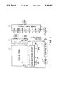
- FIG. 1 is a block diagram of a display apparatus using a driving apparatus according to the present invention
- FIG. 2 is a graph showing a relationship of operation voltages and drive potentials in the present invention
- FIG. 3 is a diagram showing a relationship among temperature, drive voltage and frequency
- FIGS. 4A and 4B are circuit diagrams showing alternative embodiments of a driving apparatus of the present invention.
- FIG. 4C is an equivalent circuit of different applifiers in FIG. 4A;
- FIG. 4D is a circuit diagram showing another embodiment of the driving apparatus of the present invention.
- FIG. 5 is a block diagram of a display apparatus using another driving apparatus according to the present invention.
- FIG. 6 is a circuit diagram of another power supply circuit used in the present invention.
- FIG. 7 is a flow chart of operation sequence for setting voltages used in the present invention.
- FIG. 8 is a circuit diagram of another power supply circuit used in the present invention.
- FIG. 9 is a block diagram of a display apparatus using a conventional driving apparatus.
- FIG. 10 is a waveform diagram showing driving waveforms for a ferroelectric liquid crystal panel as used in the present invention.
- FIG. 11 is a characteristic chart showing a relationship between the drive voltage and application time for a ferroelectric liquid crystal panel.
- FIG. 12 is a characteristic chart showing a relationship between the temperature and drive voltage for a ferroelectric liquid crystal panel.
- FIG. 1 is a block diagram showing a driving apparatus of the present invention.
- a display panel 11 includes a matrix electrode structure comprising scanning electrodes and data electrodes intersecting each other. Each intersection of the scanning electrodes and data electrodes constitutes together with a ferroelectric liquid crystal disposed between the scanning electrodes a pixel and data electrodes. The orientation of the ferroelectric liquid crystal at each pixel is modulated or controlled by the polarity, of the drive voltage applied to the pixel.
- the scanning electrodes in the display panel 11 are connected to a scanning electrode driver 12, and the data electrodes are connected to a data electrode driver 13.
- Voltages (or potentials) V DD1 , V SS1 , V DD2 , GND, V SS2 and V SS3 required for operation of the scanning electrode driver 12 and the data electrode driver 13, and the voltages (or potentials) V 1 , V 3 , Vc, V 4 and V 2 required for operation of the display panel 11 are supplied from a power supply circuit 14 to a driving unit including the scanning electrode driver 12 and the data electrode driver 13. Further, the power supply circuit 14 is supplied with two external supply voltages +V and -V.
- the logic circuit is operated by a voltage of (V DD1 -V SS1 ), and the output stage circuit is driven by a voltage of (V DD1 -V SS3 ).
- the logic circuit is operated by a voltage of (V DD2 -GND) and the output stage circuit is operated by a voltage of (V DD2 -V SS2 ).
- the scanning electrode driver 12 comprises a high-voltage process IC having a maximum rated voltage of 36 volts and including a logic circuit showing an operation frequency on the order of 30 kHz.
- the data electrode driver 13 comprises a high-voltage process IC having a maximum rated voltage of 18 volts and including a logic circuit showing an operation frequency on the order of 5 MHz.
- the operational potential ranges and drive voltage ranges are set as shown in FIG. 2.
- Vc -4 V
- V 3 -4 V to +5 V
- V 4 -4 V to -13 V
- V 2 -4 V to -22 V.
- a temperature sensor 15 comprising a temperature-sensitive resistive element is disposed on the display panel 11, and the measured data therefrom are taken in a control circuit 17 through an A/D (analog/digital) converter 16.
- the measured temperature data are compared with a data table prepared in advance, and a pulse duration ⁇ T providing an optimum drive condition based on the comparison data is outputted as a control signal while a data providing a drive voltage V 0 is supplied to a D/A converter 19.
- the data table has been prepared in consideration of the characteristics shown in FIGS. 11 and 12.
- An example of such a data table reformulated in the form of a chart is shown in FIG. 3, wherein the abscissa represents the temperature Temp.
- FIG. 4A shows an equivalent circuit of differential amplifiers contained in FIG. 4A.
- a digital drive voltage V 0 data from the control circuit 17 is supplied to the D/A converter 19 where it is converted into an analog data, which is then outputted as a voltage Vv onto a drive voltage control line v in a drive voltage generating circuit 40 in the power supply circuit 14 via a buffer amplifier 41.
- the output voltage V 1 from the differential amplifier D 1 and the output voltage V 2 from the differential amplifier D 2 are set to have a positive polarity and a negative polarity with respect to a standard voltage level set between the maximum value and minimum value of the supply voltage for driving the scanning electrode driver 12 and the data electrode driver 13.
- the voltage Vv on the drive voltage control line v is set to satisfy a relationship of -4 V (Vc) ⁇ Vv ⁇ +14 V (V DD1 ). In this embodiment, the voltage Vv is varied in the range of -4 V to +14 V depending on temperature data. Further, between the differential amplifiers' output V 1 and V 2 , four voltage division resistors R 1 , R 2 , R 3 and R 4 are connected in series, and division voltages each for 1 resistor are outputted as output voltages V 3 , Vc and V 4 in the order of higher to lower voltages. Then, these voltages are led to buffer operational amplifiers B 3 , Bc and B 4 . In this embodiment, in order to output drive voltages as shown in FIG.
- the voltages generated by the differential amplifiers D 1 , D 2 and buffer operational amplifiers B 3 , Bc and B 4 are supplied to current amplifiers I 1 , I 2 , I 3 , Ic and I 4 , among the outputs from which V 1 , Vc and V 2 are supplied to the scanning electrode driver, and V 3 , Vc and V 4 are supplied to the data electrode driver.
- a fixed voltage Vc provides a reference voltage for a voltage Vv which corresponds to an input voltage to the drive voltage generating circuit 40
- an offset voltage V offset provides a reference voltage for a voltage Eo which corresponds to an output voltage of the drive voltage generating circuit 40.
- the offset voltage can be set to an arbitrary value, preferably in a range between the maximum output voltage and the minimum output voltage of the circuit 40, particularly the mid voltage in the range.
- the current amplifiers I 1 , I 3 , Ic, I 4 and I 2 are provided so as to stably supply prescribed powers.
- a capacitor is simply disposed in parallel with each voltage division resistor as the capacitive load is small.
- a voltage drop accompanying the load switching is not negligible.
- the current amplifiers are disposed to provide larger power supplying capacities, thus providing a good regulation performance.
- circuit structure including feedback lines for connecting the outputs of the current amplifiers I 1 -I 4 and Ic to the feed lines of the differential amplifiers D 1 , D 2 , buffer operational amplifiers B 3 , B 4 and Bc, respectively, while not shown in FIG. 4, so as to remove a voltage drift of output voltages V 1 -V 4 and Vc.
- FIG. 4B shows another embodiment of the present invention wherein the output voltage V 3 is obtained by means of a voltage division resistor R 1 and the output voltage V 4 is obtained by means of a voltage division resistor R 2 .
- FIG. 4D shows another embodiment of the present invention, wherein two source voltages Vv1 and Vv2 are used in combination with differential amplifiers D 1 -D 5 and current amplifiers I 1 -I 5 .
- FIG. 5 shows another embodiment of the present invention, wherein a drive voltage generating circuit different from the one used in the power supply circuit 14 shown in FIG. 1 is used.
- a power supply circuit or unit 14 is provided with a voltage hold circuit 51, an operational amplifier 52 and a current amplifier 53.
- the voltage hold circuit 51 comprises mutually independent four circuits for the voltages V 1 , V 2 , V 3 and V 4 , respectively. According to the circuit 51, prescribed voltages V 1 , V 2 , V 3 and V 4 serially outputted from a D/A converter 19 are sampled and held by the respective circuits to set four voltages.
- FIG. 6 is a circuit diagram showing an example of the power supply circuit 14 according to this embodiment. More specifically, the power supply circuit 14 shown in FIG. 6 is one provided with a means for changing a set value of drive voltage in accordance with a temperature change, and comprises four stages including amplifiers 50a-50b, voltage hold circuits 51a-51d, operational amplifiers 52a-52d, and current amplifiers 53a-53d. As already described, set voltage data Di in the form of digital signals are sent from the above-mentioned control circuit 17 to a D/A converter 19, where the digital data are converted into analog data, which are then supplied to the voltage hold circuits 51a-51d via the amplifier 50a for V 1 /V 2 and the amplifier 50b for V 3 /V 4 .
- FIG. 7 is a flow chart showing an example sequence of control operation for sampling and holding set voltages in the voltage hold circuit 51a-51d.
- a set voltage for V 1 is set in the D/A converter 19, and a sampling signal SH 1 for V 1 is supplied to the voltage hold circuit 51a for V 1 , where a set voltage v 1 for V 1 supplied through the amplifier 50a is sampled and held.
- a similar operation is repeated by using sampling signals SH 2 , SH 3 and SH 4 to hold set voltages v 2 , v 3 and v 4 in the voltage hold circuits 51b, 51c and 51d, respectively.
- the voltages v 1 , v 2 , v 3 and v 4 set in the voltage hold circuits 51a, 51b, 51c and 51d are respectively supplied to the operational amplifiers 52a, 52b, 52c and 52d, respectively.
- the respective set values are set to satisfy the ranges of -4 V ⁇ v 1 , v 2 ⁇ 14 V, and -4 V ⁇ v 3 , v 4 ⁇ 5 V. Accordingly, as a result of differential operation by means of the operational amplifiers 52a-52d, voltages V 1 -V 4 are generated so as to satisfy the following conditions:
- the voltages generated in the operational amplifiers 52a-52d and a voltage follower operation amplifier 52e for Vc are respectively supplied to the current amplifiers 53a-53e, from which the outputs V 1 , Vc and V 2 are supplied to the scanning electrode driver 12 and the outputs V 3 , Vc and V 4 are supplied to the data electrode driver 13.
- the current amplifiers 53a-53e are provided so as to stably supply required powers.
- FIG. 8 is a circuit diagram of a voltage hold circuit for such an embodiment.
- the voltage hold circuit comprises 4 sets of a data register and a D/A converter.
- sampling signals SH 1 -SH 4 are supplied from the control circuit 17
- set voltage data Di are stored in data registers 61a-61d for voltages V 1 -V 4 .
- the data in the data registers 61a-61d are supplied to the D/A converters 62a-62d respectively connected thereto and then outputted as the above-mentioned hold voltages v 1 -v 4 in analog form.
- differentials between hold voltages v 1 -v 4 generated from set voltage data for providing voltages V 1 -V 4 and a fixed voltage Vc are respectively taken to provide positive voltages V 1 , V 3 and negative voltages V 4 , V 2 with respect to the fixed voltage Vc as the reference.
- V 1 , V 3 and negative voltages V 4 , V 2 are respectively taken to provide positive voltages V 1 , V 3 and negative voltages V 4 , V 2 with respect to the fixed voltage Vc as the reference.
- a ferroelectric liquid crystal panel may be used as the display panel 11.
- driving waveforms disclosed in, e.g., U.S. Pat. Nos. 4,655,561 and 4,709,995 in addition to those shown in FIG. 10.
Landscapes
- Engineering & Computer Science (AREA)
- Crystallography & Structural Chemistry (AREA)
- Physics & Mathematics (AREA)
- Computer Hardware Design (AREA)
- General Physics & Mathematics (AREA)
- Theoretical Computer Science (AREA)
- Chemical & Material Sciences (AREA)
- Liquid Crystal Display Device Control (AREA)
- Liquid Crystal (AREA)
- Valve Device For Special Equipments (AREA)
- Confectionery (AREA)
- Vehicle Body Suspensions (AREA)
- Electronic Switches (AREA)
- Fittings On The Vehicle Exterior For Carrying Loads, And Devices For Holding Or Mounting Articles (AREA)
- Control Of El Displays (AREA)
- Control Of Indicators Other Than Cathode Ray Tubes (AREA)
- Vending Machines For Individual Products (AREA)
- Lubrication Of Internal Combustion Engines (AREA)
Priority Applications (1)
| Application Number | Priority Date | Filing Date | Title |
|---|---|---|---|
| US07/757,009 US5317332A (en) | 1987-10-26 | 1991-09-09 | Driving apparatus for an electrode matrix suitable for a liquid crystal panel |
Applications Claiming Priority (4)
| Application Number | Priority Date | Filing Date | Title |
|---|---|---|---|
| JP62271120A JP2728876B2 (ja) | 1987-10-26 | 1987-10-26 | 表示装置 |
| JP62-271120 | 1987-10-26 | ||
| JP28415887A JP2630961B2 (ja) | 1987-11-12 | 1987-11-12 | 表示装置 |
| JP62-284158 | 1987-11-12 |
Related Child Applications (1)
| Application Number | Title | Priority Date | Filing Date |
|---|---|---|---|
| US07/757,009 Continuation US5317332A (en) | 1987-10-26 | 1991-09-09 | Driving apparatus for an electrode matrix suitable for a liquid crystal panel |
Publications (1)
| Publication Number | Publication Date |
|---|---|
| US5066945A true US5066945A (en) | 1991-11-19 |
Family
ID=26549544
Family Applications (2)
| Application Number | Title | Priority Date | Filing Date |
|---|---|---|---|
| US07/262,576 Expired - Lifetime US5066945A (en) | 1987-10-26 | 1988-10-25 | Driving apparatus for an electrode matrix suitable for a liquid crystal panel |
| US07/757,009 Expired - Lifetime US5317332A (en) | 1987-10-26 | 1991-09-09 | Driving apparatus for an electrode matrix suitable for a liquid crystal panel |
Family Applications After (1)
| Application Number | Title | Priority Date | Filing Date |
|---|---|---|---|
| US07/757,009 Expired - Lifetime US5317332A (en) | 1987-10-26 | 1991-09-09 | Driving apparatus for an electrode matrix suitable for a liquid crystal panel |
Country Status (8)
| Country | Link |
|---|---|
| US (2) | US5066945A (de) |
| EP (1) | EP0314084B1 (de) |
| AT (1) | ATE116466T1 (de) |
| AU (1) | AU605931B2 (de) |
| CA (1) | CA1331813C (de) |
| DE (1) | DE3852610T2 (de) |
| ES (1) | ES2065327T3 (de) |
| GR (1) | GR3015613T3 (de) |
Cited By (28)
| Publication number | Priority date | Publication date | Assignee | Title |
|---|---|---|---|---|
| US5243333A (en) * | 1991-07-29 | 1993-09-07 | Nec Corporation | Driver for active matrix type liquid crystal display device |
| US5250937A (en) * | 1990-03-08 | 1993-10-05 | Hitachi, Ltd. | Half tone liquid crystal display circuit with an A.C. voltage divider for drivers |
| US5276542A (en) * | 1991-04-15 | 1994-01-04 | Canon Kabushiki Kaisha | Ferroelectric liquid crystal apparatus having temperature compensation control circuit |
| US5576737A (en) * | 1993-12-22 | 1996-11-19 | Seiko Epson Corporation | Liquid crystal drive device, liquid crystal display device, and liquid crystal drive method |
| US5583531A (en) * | 1991-05-21 | 1996-12-10 | Sharp Kabushiki Kaisha | Method of driving a display apparatus |
| US5594463A (en) * | 1993-07-19 | 1997-01-14 | Pioneer Electronic Corporation | Driving circuit for display apparatus, and method of driving display apparatus |
| US5606343A (en) * | 1991-07-24 | 1997-02-25 | Canon Kabushiki Kaisha | Display device |
| US5621426A (en) * | 1993-03-24 | 1997-04-15 | Sharp Kabushiki Kaisha | Display apparatus and driving circuit for driving the same |
| US5726722A (en) * | 1993-01-19 | 1998-03-10 | Canon Kabushiki Kaisha | Light source for display device |
| US5739808A (en) * | 1994-10-28 | 1998-04-14 | Canon Kabushiki Kaisha | Display control method and apparatus |
| US5745092A (en) * | 1993-12-22 | 1998-04-28 | Seiko Epson Corporation | Liquid-Crystal display system and power supply method that supply different logic source voltages to signal and scan drivers |
| US5748170A (en) * | 1992-02-03 | 1998-05-05 | Nikon Corporation | Display driving apparatus with automatic drive voltage optimization |
| US5751278A (en) * | 1990-08-10 | 1998-05-12 | Sharp Kabushiki Kaisha | Clocking method and apparatus for display device with calculation operation |
| US5798741A (en) * | 1994-12-28 | 1998-08-25 | Sharp Kabushiki Kaisha | Power source for driving liquid crystal |
| US5856815A (en) * | 1991-10-07 | 1999-01-05 | Fujitsu Limited | Method of driving surface-stabilized ferroelectric liquid crystal display element for increasing the number of gray scales |
| US5923312A (en) * | 1994-10-14 | 1999-07-13 | Sharp Kabushiki Kaisha | Driving circuit used in display apparatus and liquid crystal display apparatus using such driving circuit |
| US5936604A (en) * | 1994-04-21 | 1999-08-10 | Casio Computer Co., Ltd. | Color liquid crystal display apparatus and method for driving the same |
| US5999156A (en) * | 1995-06-15 | 1999-12-07 | Sharp Kabushiki Kaisha | Matrix electrode structural display element driving unit |
| US6037921A (en) * | 1992-05-19 | 2000-03-14 | Canon Kabushiki Kaisha | Display control apparatus with independent information receivers |
| US6037920A (en) * | 1997-03-13 | 2000-03-14 | Canon Kabushiki Kaisha | Liquid crystal apparatus and driving method therefor |
| US6054971A (en) * | 1991-02-20 | 2000-04-25 | Canon Kabushiki Kaisha | Display apparatus |
| US6151005A (en) * | 1992-10-07 | 2000-11-21 | Hitachi, Ltd. | Liquid-crystal display system having a driver circuit capable of multi-color display |
| US6151006A (en) * | 1994-07-27 | 2000-11-21 | Sharp Kabushiki Kaisha | Active matrix type display device and a method for driving the same |
| US6433769B1 (en) | 2000-01-04 | 2002-08-13 | International Business Machines Corporation | Compensation circuit for display contrast voltage control |
| US20080036441A1 (en) * | 2006-08-11 | 2008-02-14 | Innocom Technology (Shenzhen) Co., Ltd. Innolux Display Corp. | Voltage regulating circuit having voltage stabilizing circuits |
| US20090278780A1 (en) * | 2008-05-08 | 2009-11-12 | Chunghwa Picture Tubes, Ltd. | Liquid crystal display and switching voltage controlling circuit thereof |
| US20130162618A1 (en) * | 2009-11-23 | 2013-06-27 | Silicon Works Co., Ltd | Output voltage stabilization circuit of display device driving circuit |
| US12147109B2 (en) | 2021-06-17 | 2024-11-19 | Stanley Electric Co., Ltd. | Apparatus for controlling temperature of heater, method for controlling temperature of heater, liquid crystal apparatus |
Families Citing this family (23)
| Publication number | Priority date | Publication date | Assignee | Title |
|---|---|---|---|---|
| CA1319767C (en) * | 1987-11-26 | 1993-06-29 | Canon Kabushiki Kaisha | Display apparatus |
| DE69022891T2 (de) * | 1989-06-15 | 1996-05-15 | Matsushita Electric Ind Co Ltd | Gerät zur Kompensierung von Videosignalen. |
| DE4009404A1 (de) * | 1990-03-23 | 1991-09-26 | Telefonbau & Normalzeit Gmbh | Schaltungsanordnung zur spannungsversorgung der zeilen- und spaltentreiber einer fluessigkristallanzeigevorrichtung |
| JP2695981B2 (ja) * | 1990-10-05 | 1998-01-14 | 株式会社東芝 | 液晶表示器駆動電源回路 |
| IT221756Z2 (it) * | 1991-03-22 | 1994-10-20 | Gallone Cesare | Dispositivo a display luminosi per apparecchiature elettriche |
| EP0537428B1 (de) * | 1991-08-02 | 1998-09-30 | Canon Kabushiki Kaisha | Anzeigesteuergerät |
| DE69319943T2 (de) * | 1992-02-28 | 1999-02-11 | Canon K.K., Tokio/Tokyo | Flüssigkristallanzeigegerät |
| JPH08106272A (ja) * | 1994-10-03 | 1996-04-23 | Semiconductor Energy Lab Co Ltd | 表示装置駆動回路 |
| JP3568644B2 (ja) * | 1995-09-01 | 2004-09-22 | シャープ株式会社 | 液晶表示装置およびその駆動方法 |
| US5999157A (en) * | 1995-12-27 | 1999-12-07 | Canon Kabushiki Kaisha | Suppressing liquid crystal movement based on the relationship between a display pattern and a driving waveform |
| US5956010A (en) * | 1996-05-31 | 1999-09-21 | Canon Kabushiki Kaisha | Liquid crystal apparatus and driving method |
| JPH1039772A (ja) * | 1996-07-29 | 1998-02-13 | Mitsubishi Electric Corp | 投写型液晶表示装置 |
| JP3317871B2 (ja) * | 1997-03-27 | 2002-08-26 | シャープ株式会社 | 表示装置 |
| JP3693464B2 (ja) * | 1997-05-22 | 2005-09-07 | ローム株式会社 | 表示パネルの駆動装置 |
| JPH11184444A (ja) * | 1997-12-24 | 1999-07-09 | Oki Micro Design Miyazaki Co Ltd | 液晶表示装置駆動用集積回路 |
| US6268839B1 (en) * | 1998-05-12 | 2001-07-31 | Kent State University | Drive schemes for gray scale bistable cholesteric reflective displays |
| JP3016143B2 (ja) * | 1998-07-27 | 2000-03-06 | セイコーインスツルメンツ株式会社 | 液晶用電源回路 |
| JP2000221468A (ja) | 1999-01-29 | 2000-08-11 | Citizen Watch Co Ltd | 液晶駆動装置 |
| US7023409B2 (en) | 2001-02-09 | 2006-04-04 | Kent Displays, Incorporated | Drive schemes for gray scale bistable cholesteric reflective displays utilizing variable frequency pulses |
| US6809978B2 (en) | 2002-05-13 | 2004-10-26 | Infineon Technologies Ag | Implementation of a temperature sensor to control internal chip voltages |
| TWI340945B (en) * | 2006-12-01 | 2011-04-21 | Chimei Innolux Corp | Liquid crystal display |
| KR20170015752A (ko) * | 2015-07-31 | 2017-02-09 | 삼성디스플레이 주식회사 | 감마기준전압 생성부 및 이를 포함하는 표시장치 |
| DE102021130619B4 (de) | 2021-11-23 | 2025-09-11 | UNO MINDA Europe GmbH | Vorrichtung und Baugruppe zum Erzeugen von Bildern auf einer Projektionsfläche |
Citations (10)
| Publication number | Priority date | Publication date | Assignee | Title |
|---|---|---|---|---|
| US4186436A (en) * | 1977-01-27 | 1980-01-29 | Canon Kabushiki Kaisha | Booster circuit |
| US4532504A (en) * | 1982-09-09 | 1985-07-30 | Sperry Corporation | Slew length timer |
| US4548476A (en) * | 1983-01-14 | 1985-10-22 | Canon Kabushiki Kaisha | Time-sharing driving method for ferroelectric liquid crystal display |
| US4622590A (en) * | 1983-02-28 | 1986-11-11 | Seigo Togashi | Method of driving a display device |
| US4622635A (en) * | 1984-02-13 | 1986-11-11 | Automated Controls Inc. | Portable display and control terminal for wells |
| US4655561A (en) * | 1983-04-19 | 1987-04-07 | Canon Kabushiki Kaisha | Method of driving optical modulation device using ferroelectric liquid crystal |
| GB2188471A (en) * | 1986-03-19 | 1987-09-30 | Sharp Kk | L C D devices |
| US4709995A (en) * | 1984-08-18 | 1987-12-01 | Canon Kabushiki Kaisha | Ferroelectric display panel and driving method therefor to achieve gray scale |
| US4714921A (en) * | 1985-02-06 | 1987-12-22 | Canon Kabushiki Kaisha | Display panel and method of driving the same |
| US4769639A (en) * | 1985-09-25 | 1988-09-06 | Casio Computer Co., Ltd. | Liquid crystal drive circuit for driving a liquid crystal display element having scanning and signal electrodes arranged in matrix form |
-
1988
- 1988-10-25 EP EP88117786A patent/EP0314084B1/de not_active Expired - Lifetime
- 1988-10-25 ES ES88117786T patent/ES2065327T3/es not_active Expired - Lifetime
- 1988-10-25 DE DE3852610T patent/DE3852610T2/de not_active Expired - Fee Related
- 1988-10-25 AT AT88117786T patent/ATE116466T1/de not_active IP Right Cessation
- 1988-10-25 US US07/262,576 patent/US5066945A/en not_active Expired - Lifetime
- 1988-10-26 CA CA000581314A patent/CA1331813C/en not_active Expired - Fee Related
- 1988-10-26 AU AU24414/88A patent/AU605931B2/en not_active Ceased
-
1991
- 1991-09-09 US US07/757,009 patent/US5317332A/en not_active Expired - Lifetime
-
1995
- 1995-03-23 GR GR950400689T patent/GR3015613T3/el unknown
Patent Citations (10)
| Publication number | Priority date | Publication date | Assignee | Title |
|---|---|---|---|---|
| US4186436A (en) * | 1977-01-27 | 1980-01-29 | Canon Kabushiki Kaisha | Booster circuit |
| US4532504A (en) * | 1982-09-09 | 1985-07-30 | Sperry Corporation | Slew length timer |
| US4548476A (en) * | 1983-01-14 | 1985-10-22 | Canon Kabushiki Kaisha | Time-sharing driving method for ferroelectric liquid crystal display |
| US4622590A (en) * | 1983-02-28 | 1986-11-11 | Seigo Togashi | Method of driving a display device |
| US4655561A (en) * | 1983-04-19 | 1987-04-07 | Canon Kabushiki Kaisha | Method of driving optical modulation device using ferroelectric liquid crystal |
| US4622635A (en) * | 1984-02-13 | 1986-11-11 | Automated Controls Inc. | Portable display and control terminal for wells |
| US4709995A (en) * | 1984-08-18 | 1987-12-01 | Canon Kabushiki Kaisha | Ferroelectric display panel and driving method therefor to achieve gray scale |
| US4714921A (en) * | 1985-02-06 | 1987-12-22 | Canon Kabushiki Kaisha | Display panel and method of driving the same |
| US4769639A (en) * | 1985-09-25 | 1988-09-06 | Casio Computer Co., Ltd. | Liquid crystal drive circuit for driving a liquid crystal display element having scanning and signal electrodes arranged in matrix form |
| GB2188471A (en) * | 1986-03-19 | 1987-09-30 | Sharp Kk | L C D devices |
Non-Patent Citations (2)
| Title |
|---|
| I.E.E.E. Transactions on consumer Electronics, vol. CE 28, No. 3, Aug. 1982, pp. 196 200, Fujii, T., et al. Dot Matrix LCD Module For Graphic Display . * |
| I.E.E.E. Transactions on consumer Electronics, vol. CE-28, No. 3, Aug. 1982, pp. 196-200, Fujii, T., et al. "Dot Matrix LCD Module For Graphic Display". |
Cited By (31)
| Publication number | Priority date | Publication date | Assignee | Title |
|---|---|---|---|---|
| US5250937A (en) * | 1990-03-08 | 1993-10-05 | Hitachi, Ltd. | Half tone liquid crystal display circuit with an A.C. voltage divider for drivers |
| US5751278A (en) * | 1990-08-10 | 1998-05-12 | Sharp Kabushiki Kaisha | Clocking method and apparatus for display device with calculation operation |
| US6054971A (en) * | 1991-02-20 | 2000-04-25 | Canon Kabushiki Kaisha | Display apparatus |
| US5276542A (en) * | 1991-04-15 | 1994-01-04 | Canon Kabushiki Kaisha | Ferroelectric liquid crystal apparatus having temperature compensation control circuit |
| US5583531A (en) * | 1991-05-21 | 1996-12-10 | Sharp Kabushiki Kaisha | Method of driving a display apparatus |
| US5606343A (en) * | 1991-07-24 | 1997-02-25 | Canon Kabushiki Kaisha | Display device |
| US5243333A (en) * | 1991-07-29 | 1993-09-07 | Nec Corporation | Driver for active matrix type liquid crystal display device |
| US5856815A (en) * | 1991-10-07 | 1999-01-05 | Fujitsu Limited | Method of driving surface-stabilized ferroelectric liquid crystal display element for increasing the number of gray scales |
| US5748170A (en) * | 1992-02-03 | 1998-05-05 | Nikon Corporation | Display driving apparatus with automatic drive voltage optimization |
| US6037921A (en) * | 1992-05-19 | 2000-03-14 | Canon Kabushiki Kaisha | Display control apparatus with independent information receivers |
| US6151005A (en) * | 1992-10-07 | 2000-11-21 | Hitachi, Ltd. | Liquid-crystal display system having a driver circuit capable of multi-color display |
| US5726722A (en) * | 1993-01-19 | 1998-03-10 | Canon Kabushiki Kaisha | Light source for display device |
| US5621426A (en) * | 1993-03-24 | 1997-04-15 | Sharp Kabushiki Kaisha | Display apparatus and driving circuit for driving the same |
| US5594463A (en) * | 1993-07-19 | 1997-01-14 | Pioneer Electronic Corporation | Driving circuit for display apparatus, and method of driving display apparatus |
| US5745092A (en) * | 1993-12-22 | 1998-04-28 | Seiko Epson Corporation | Liquid-Crystal display system and power supply method that supply different logic source voltages to signal and scan drivers |
| US5576737A (en) * | 1993-12-22 | 1996-11-19 | Seiko Epson Corporation | Liquid crystal drive device, liquid crystal display device, and liquid crystal drive method |
| US5936604A (en) * | 1994-04-21 | 1999-08-10 | Casio Computer Co., Ltd. | Color liquid crystal display apparatus and method for driving the same |
| US6151006A (en) * | 1994-07-27 | 2000-11-21 | Sharp Kabushiki Kaisha | Active matrix type display device and a method for driving the same |
| CN1097812C (zh) * | 1994-10-14 | 2003-01-01 | 夏普公司 | 显示装置中用的驱动电路及用该驱动电路的液晶显示装置 |
| US5923312A (en) * | 1994-10-14 | 1999-07-13 | Sharp Kabushiki Kaisha | Driving circuit used in display apparatus and liquid crystal display apparatus using such driving circuit |
| US5739808A (en) * | 1994-10-28 | 1998-04-14 | Canon Kabushiki Kaisha | Display control method and apparatus |
| US5798741A (en) * | 1994-12-28 | 1998-08-25 | Sharp Kabushiki Kaisha | Power source for driving liquid crystal |
| US5999156A (en) * | 1995-06-15 | 1999-12-07 | Sharp Kabushiki Kaisha | Matrix electrode structural display element driving unit |
| US6037920A (en) * | 1997-03-13 | 2000-03-14 | Canon Kabushiki Kaisha | Liquid crystal apparatus and driving method therefor |
| US6433769B1 (en) | 2000-01-04 | 2002-08-13 | International Business Machines Corporation | Compensation circuit for display contrast voltage control |
| US20080036441A1 (en) * | 2006-08-11 | 2008-02-14 | Innocom Technology (Shenzhen) Co., Ltd. Innolux Display Corp. | Voltage regulating circuit having voltage stabilizing circuits |
| US20090278780A1 (en) * | 2008-05-08 | 2009-11-12 | Chunghwa Picture Tubes, Ltd. | Liquid crystal display and switching voltage controlling circuit thereof |
| US8125478B2 (en) * | 2008-05-08 | 2012-02-28 | Chunghwa Picture Tubes, Ltd. | Liquid crystal display and switching voltage controlling circuit thereof for reducing occurrence of color errors |
| US20130162618A1 (en) * | 2009-11-23 | 2013-06-27 | Silicon Works Co., Ltd | Output voltage stabilization circuit of display device driving circuit |
| US9143090B2 (en) * | 2009-11-23 | 2015-09-22 | Silicon Works Co., Ltd. | Output voltage stabilization circuit of display device driving circuit |
| US12147109B2 (en) | 2021-06-17 | 2024-11-19 | Stanley Electric Co., Ltd. | Apparatus for controlling temperature of heater, method for controlling temperature of heater, liquid crystal apparatus |
Also Published As
| Publication number | Publication date |
|---|---|
| ATE116466T1 (de) | 1995-01-15 |
| EP0314084A3 (en) | 1990-05-09 |
| EP0314084B1 (de) | 1994-12-28 |
| DE3852610T2 (de) | 1995-05-18 |
| ES2065327T3 (es) | 1995-02-16 |
| CA1331813C (en) | 1994-08-30 |
| AU605931B2 (en) | 1991-01-24 |
| EP0314084A2 (de) | 1989-05-03 |
| GR3015613T3 (en) | 1995-06-30 |
| US5317332A (en) | 1994-05-31 |
| DE3852610D1 (de) | 1995-02-09 |
| AU2441488A (en) | 1989-04-27 |
Similar Documents
| Publication | Publication Date | Title |
|---|---|---|
| US5066945A (en) | Driving apparatus for an electrode matrix suitable for a liquid crystal panel | |
| KR960009443B1 (ko) | 표시장치용 구동회로 | |
| US5033822A (en) | Liquid crystal apparatus with temperature compensation control circuit | |
| US5010326A (en) | Circuit for driving a liquid crystal display device | |
| KR100348644B1 (ko) | 중간 탭을 구비하는 전압 증배기 | |
| US5625387A (en) | Gray voltage generator for liquid crystal display capable of controlling a viewing angle | |
| US5442370A (en) | System for driving a liquid crystal display device | |
| KR960008104B1 (ko) | 표시장치의 구동방법과 표시장치의 구동회로 및 이를 이용한 표시장치 | |
| US7078864B2 (en) | Display apparatus and power supply device for displaying | |
| US20020195955A1 (en) | Display apparatus and power supply device for displaying | |
| EP0678846B1 (de) | Verbesserung zur Energiesparung in einer Anzeigevorrichtung mit aktiver Matrix mit Grauwerten | |
| US5343217A (en) | Method for driving a ferroelectric liquid crystal displays and bias voltage circuit therefor | |
| EP0229716B1 (de) | Schaltung zum Abgleichen von Kristalländerungen für Flüssigkristallanzeigegerät | |
| KR100864491B1 (ko) | 액정 표시 장치의 구동 장치 | |
| US6084580A (en) | Voltage generating circuit and liquid crystal display device incorporating the voltage generating circuit | |
| US6731265B1 (en) | Display apparatus and method for driving the same | |
| US6124839A (en) | Liquid crystal display driving circuit and liquid crystal display having parallel resonant circuit for reduced power consumption | |
| EP0544427B1 (de) | Steuerschaltung für eine Anzeigeeinheit mit digitaler Sourcesteuerung zur Erzeugung von Mehrfachpegelsteuerspannungen aus einer einzelnen externen Energiequelle | |
| JP2630961B2 (ja) | 表示装置 | |
| EP0477014A2 (de) | Anzeigegerät mit Helligkeitsteuerung | |
| EP0447919B1 (de) | Steuereinrichtung für eine Bildpunktmatrixanzeige | |
| JP3520870B2 (ja) | 液晶表示装置及びその電源回路 | |
| JP2725003B2 (ja) | 液晶表示装置の駆動方法 | |
| JP2728876B2 (ja) | 表示装置 | |
| JP2708946B2 (ja) | 表示電源回路 |
Legal Events
| Date | Code | Title | Description |
|---|---|---|---|
| AS | Assignment |
Owner name: CANON KABUSHIKI KAISHA, 3-30-2 SHIMOMARUKO, OHTA-K Free format text: ASSIGNMENT OF ASSIGNORS INTEREST.;ASSIGNORS:KANNO, HIDEO;INOUE, HIROSHI;MIZUTOME, ATSUSHI;REEL/FRAME:004991/0136 Effective date: 19881019 |
|
| STCF | Information on status: patent grant |
Free format text: PATENTED CASE |
|
| CC | Certificate of correction | ||
| FPAY | Fee payment |
Year of fee payment: 4 |
|
| FEPP | Fee payment procedure |
Free format text: PAYER NUMBER DE-ASSIGNED (ORIGINAL EVENT CODE: RMPN); ENTITY STATUS OF PATENT OWNER: LARGE ENTITY Free format text: PAYOR NUMBER ASSIGNED (ORIGINAL EVENT CODE: ASPN); ENTITY STATUS OF PATENT OWNER: LARGE ENTITY |
|
| FPAY | Fee payment |
Year of fee payment: 8 |
|
| FPAY | Fee payment |
Year of fee payment: 12 |
|
| REMI | Maintenance fee reminder mailed |