US5124582A - Bi-cmos circuit with high-speed active pull-down output currents - Google Patents
Bi-cmos circuit with high-speed active pull-down output currents Download PDFInfo
- Publication number
- US5124582A US5124582A US07/605,325 US60532590A US5124582A US 5124582 A US5124582 A US 5124582A US 60532590 A US60532590 A US 60532590A US 5124582 A US5124582 A US 5124582A
- Authority
- US
- United States
- Prior art keywords
- transistor
- base
- current
- gate electrode
- channel mos
- Prior art date
- Legal status (The legal status is an assumption and is not a legal conclusion. Google has not performed a legal analysis and makes no representation as to the accuracy of the status listed.)
- Expired - Lifetime
Links
Images


Classifications
-
- H—ELECTRICITY
- H03—ELECTRONIC CIRCUITRY
- H03K—PULSE TECHNIQUE
- H03K19/00—Logic circuits, i.e. having at least two inputs acting on one output; Inverting circuits
- H03K19/02—Logic circuits, i.e. having at least two inputs acting on one output; Inverting circuits using specified components
- H03K19/08—Logic circuits, i.e. having at least two inputs acting on one output; Inverting circuits using specified components using semiconductor devices
- H03K19/094—Logic circuits, i.e. having at least two inputs acting on one output; Inverting circuits using specified components using semiconductor devices using field-effect transistors
-
- H—ELECTRICITY
- H03—ELECTRONIC CIRCUITRY
- H03K—PULSE TECHNIQUE
- H03K19/00—Logic circuits, i.e. having at least two inputs acting on one output; Inverting circuits
- H03K19/01—Modifications for accelerating switching
- H03K19/013—Modifications for accelerating switching in bipolar transistor circuits
- H03K19/0136—Modifications for accelerating switching in bipolar transistor circuits by means of a pull-up or down element
-
- H—ELECTRICITY
- H03—ELECTRONIC CIRCUITRY
- H03K—PULSE TECHNIQUE
- H03K19/00—Logic circuits, i.e. having at least two inputs acting on one output; Inverting circuits
- H03K19/02—Logic circuits, i.e. having at least two inputs acting on one output; Inverting circuits using specified components
- H03K19/08—Logic circuits, i.e. having at least two inputs acting on one output; Inverting circuits using specified components using semiconductor devices
- H03K19/094—Logic circuits, i.e. having at least two inputs acting on one output; Inverting circuits using specified components using semiconductor devices using field-effect transistors
- H03K19/0944—Logic circuits, i.e. having at least two inputs acting on one output; Inverting circuits using specified components using semiconductor devices using field-effect transistors using MOSFET or insulated gate field-effect transistors, i.e. IGFET
- H03K19/09448—Logic circuits, i.e. having at least two inputs acting on one output; Inverting circuits using specified components using semiconductor devices using field-effect transistors using MOSFET or insulated gate field-effect transistors, i.e. IGFET in combination with bipolar transistors [BIMOS]
Definitions
- the present invention relates to a logic circuit, and more particularly to a logic circuit of Bi-CMOS construction used for driving capacitive load.
- a logic circuit of high performance can be made by building a bipolar circuit having advantages of high accuracy analog processing and large power drive and a CMOS circuit having advantages of high integration and low power consumption, together on the same IC chip.
- FIG. 7 schematically shows a conventional logic circuit which forms an inverter with the Bi-CMOS process.
- M n1 is an input transistor made from an N-channel MOS transistor
- Q 1 and Q 2 are off-buffer transistors made from bipolar transistors
- Q 3 is an output transistor made from a bipolar transistor.
- R 1 through R 4 are resistors
- C is capacitive load, V IN an input signal, and V OUT an output signal.
- Q 1 and Q 3 normally comprise transistors with schottky barriers, and alternatively, the areas of Q 2 and Q 3 are increased.
- a Bi-CMOS circuit comprising a first transistor made from an N-channel MOS transistor that is turned on and off in response to the logic state of an input signal and that supplies a first current to the base of an output transistor when the first transistor is turned on, and an active pull-down current supplying means connected to the gate electrode of the first transistor and for supplying a second current, which is active pull-down current, to the base of the output transistor so that the first and second currents can be supplied to the base of the output transistor.
- the active pull-down current supplying means may comprise a second transistor made from a P-channel MOS transistor and having its gate electrode connected to the gate electrode of the first transistor, a third transistor made from an N-channel MOS transistor and having its gate electrode connected to the gate electrode of the second transistor, the third transistor being connected in series with the second transistor, and a fourth transistor made from a bipolar transistor and having its base connected to the third transistor and its emitter connected to the base of the output transistor.
- the second transistor may be substantially identical in area with the third transistor.
- the second transistor may also be greater in area than the third transistor.
- the active pull-down current supplying means may also be comprise a second transistor made from a P-channel MOS transistor and having its gate electrode connected to the gate electrode of the first transistor, a third transistor made from an N-channel MOS transistor and having its gate electrode connected to the gate electrode of the second transistor, the third transistor being connected in series with the second transistor, a fourth transistor made from a P-channel MOS transistor, a fifth transistor made from an N-channel MOS transistor and having its gate electrode connected to the gate electrode of the fourth transistor, the fifth transistor being connected in series with the fourth transistor, a line between the second and third transistors being connected to a line between the fourth and fifth transistors, and a sixth transistor made from a bipolar transistor and having its base connected to the fifth transistor and its emitter connected to the base of the output transistor.
- the second and third transistors are turned on, and the fourth transistor made from a bipolar transistor is turned on by the current that flows through the second and third transistors. Consequently, the current that flows through both first transistor and the fourth transistor is supplied to the base of the output transistor (corresponding to the transistor Q 3 ), and the turn-on speed of the output transistor is thus made faster.
- a Bi-CMOS circuit comprising first and second transistors respectively made from a P-channel MOS transistor and an N-channel MOS transistor that are turned on and off in response to the logic state of an input signal and that supplies a first current to the base of an output transistor when the first and second transistors are turned on, and an active pull-down current supplying means connected to the gate electrodes of the first and second transistors and for supplying a second current, which is active pull-down current, to the base of the output transistor so that the first and second currents can be supplied to the base of the output transistor.
- a Bi-CMOS circuit comprising a first transistor made from an N-channel MOS transistor that is turned on and off in response to the logic state of an input signal and that supplies a first current to the base of a first output transistor when the first transistor is turned on, second and third transistors respectively made from a P-channel MOS transistor and an N-channel MOS transistor that are turned on and off in response to the logic state of the input signal and that supplies a second current to the base of a second output transistor when the second and third transistors are turned on, a first active pull-down current supplying means connected to the gate electrode of the first transistor and for supplying a third current, which is an active pull-down current, to the base of the first output transistor so that the first and third currents can be supplied to the base of the first output transistor, and a second active pull-down current supplying means connected to the gate electrodes of the second and third transistors and for supplying a fourth current, which is an active pull-down current, to
- the third current supplied through the first active pull-down current supplying means is an supplied to the base of the first output transistor when the input signal makes a transition from a low to a high, while the fourth current supplied through the second active pull-down current supplying means is supplied to the base of the second output transistor when the input signal makes a transition from a high to a low.
- FIG. 1 is a schematic view illustrating an embodiment of a Bi-CMOS circuit in accordance with the present invention
- FIG. 2 is a timing diagram of the FIG. 1 embodiment
- FIG. 3 is a schematic view illustrating another embodiment of the Bi-CMOS circuit in accordance with the present invention.
- FIG. 4 is a waveform diagram of the output signals from the FIG. 1 embodiment
- FIG. 5 is a schematic view illustrating a third embodiment of the Bi-CMOS circuit in accordance with the present invention.
- FIG. 6 is a schematic view illustrating a fourth embodiment of the Bi-CMOS circuit in accordance with the present invention.
- FIG. 7 is a schematic diagram of a conventional logic circuit.
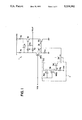
- Reference numeral 1 denotes a gate part that functions as an inverter.
- the gate part 1 comprises off-buffer transistors Q 1 and Q 2 each made from a bipolar transistor, an output transistor Q 3 made from a bipolar transistor, and an input transistor (first transistor M n1 made from an N-channel MOS transistor.
- the logic state of an output signal V OUT of the inverter is determined by turning on either the off-buffer transistors Q 1 and Q 2 of high level side or the output transistor Q 3 of low level side with an ON/OFF operation of the input transistor M n1 .
- the input signal V IN is in a logic low state
- the input transistor M n1 is turned off and the off-buffer transistors Q 1 and Q 2 are turned on. Consequently, the output signal V OUT goes to a logic high state.
- the input signal V IN is in a logic high state
- the input transistor M n1 is turned on, a base current I B is supplied to the output transistor Q 3 , and therefore the output transistor Q 3 is turned on. Consequently, the output signal V OUT goes to a logic low state.
- Reference numeral 2 is an auxiliary drive circuit which is the gist of the present invention.
- the auxiliary drive circuit 2 comprises a P-channel MOS transistor (second transistor) M p1 , an N-channel MOS transistor (third transistor) M n2 , and a resistor R 5 which are connected in series.
- the auxiliary drive circuit 2 further comprises a bipolar transistor Q 4 (fourth transistor) having its base connected to the line between M n2 and R 5 and its emitter connected to the base of the output transistor Q 3 .
- the area of M p1 is substantially the same as that of M n2 .
- the current I B 40 functions as active pull-down current, makes the turn-on of Q 3 deep, and can rapidly pull out a wiring load capacity connected to V OUT . As a result, high-speed operation can be performed.
- the base current of the output transistor Q 3 is increased by supplying the current from Q 4 of the auxiliary drive circuit 2. Consequently, the turn-on speed of Q 3 can be made faster and therefore t PHL can be shortened.
- the above described embodiment is applied to an inverter, it is noted that it may also be applied to a logic circuit in which input and output signals V IN and V OUT change in the same logic state.
- the area of M n2 is made smaller than that of M p1 so that the turn-on speed of M n2 can be made slower when V IN makes a transition from a high to a low. Consequently, the base current of Q 3 can be increased in the same way.
- FIG. 3 schematically shows another embodiment of the auxiliary drive circuit 2 of FIG. 1.
- an auxiliary drive circuit 2' is provided at its input side with an inverter stage 3 comprising a P-channel MOS transistor M p2 and an N-channel MOS transistor M n3 .
- the input signal V IN makes a transition from a high to a low
- the turn-on speed of M n2 can be made slower.
- the base current of Q 3 can be increased.
- FIG. 4 illustrates the waveform of the output signal V OUT .
- V cc was set to 5.5 V, 5.0 V and 4.5 V, and each t PHL according to the present invention was compared with that of the conventional logic circuit. It will be understood from FIG. 4 that, with the rapid turn-on speed of Q 3 , the high-to-low transition according to the present invention is faster than that of the conventional logic circuit.
- FIG. 5 schematically illustrates a Bi-CMOS circuit to which the present invention is applied to improve t PLH .
- the same reference characters will be applied to the same parts as FIG. 1 and therefore a detailed description will not be given.
- the base current I B' of Q 4 is added to the base current I B" of Q 1 , so that the turn-on speed of Q 2 is made faster and the propagation delay time t PLH of the output signal V OUT is shortened.
- the present invention is applicable to improve both t PHL and t PLH .
- FIG. 6 schematically illustrates a Bi-CMOS circuit in which both t PHL and t PLH are shortened in accordance with the present invention.
- the base currents of Q 2 and Q 3 are increased in the same manner as those of the embodiments of FIGS. 1 and 5, so both t PHL and t PLH can be shortened.
Landscapes
- Engineering & Computer Science (AREA)
- Physics & Mathematics (AREA)
- Computer Hardware Design (AREA)
- Computing Systems (AREA)
- General Engineering & Computer Science (AREA)
- Mathematical Physics (AREA)
- Power Engineering (AREA)
- Logic Circuits (AREA)
Applications Claiming Priority (2)
| Application Number | Priority Date | Filing Date | Title |
|---|---|---|---|
| JP1286119A JP2820980B2 (ja) | 1989-11-02 | 1989-11-02 | 論理回路 |
| JP1-286119 | 1989-11-02 |
Publications (1)
| Publication Number | Publication Date |
|---|---|
| US5124582A true US5124582A (en) | 1992-06-23 |
Family
ID=17700179
Family Applications (1)
| Application Number | Title | Priority Date | Filing Date |
|---|---|---|---|
| US07/605,325 Expired - Lifetime US5124582A (en) | 1989-11-02 | 1990-10-30 | Bi-cmos circuit with high-speed active pull-down output currents |
Country Status (5)
| Country | Link |
|---|---|
| US (1) | US5124582A (de) |
| EP (1) | EP0426547B1 (de) |
| JP (1) | JP2820980B2 (de) |
| KR (1) | KR930007566B1 (de) |
| DE (1) | DE69029922T2 (de) |
Cited By (6)
| Publication number | Priority date | Publication date | Assignee | Title |
|---|---|---|---|---|
| US5218243A (en) * | 1991-11-20 | 1993-06-08 | National Semiconductor Corporation | Bicmos ttl output buffer circuit with reduced power dissipation |
| US5489861A (en) * | 1993-12-20 | 1996-02-06 | National Semiconductor Corporation | High power, edge controlled output buffer |
| US5659261A (en) * | 1991-10-30 | 1997-08-19 | Harris Corporation | Analog-to-digital converter and output driver |
| US5691544A (en) * | 1992-06-24 | 1997-11-25 | Robotic Vision Systems, Inc. | Apparatus for obtaining three-dimensional data from multiple parts or devices in a multi-pocketed tray |
| US5793051A (en) * | 1995-06-07 | 1998-08-11 | Robotic Vision Systems, Inc. | Method for obtaining three-dimensional data from semiconductor devices in a row/column array and control of manufacturing of same with data to eliminate manufacturing errors |
| US5994755A (en) * | 1991-10-30 | 1999-11-30 | Intersil Corporation | Analog-to-digital converter and method of fabrication |
Families Citing this family (1)
| Publication number | Priority date | Publication date | Assignee | Title |
|---|---|---|---|---|
| EP0629047A3 (de) * | 1993-06-02 | 1995-03-29 | Philips Electronics Nv | BICMOS Ausgangstreiber für hohe Ausgangsströme und geringe Ausgangsspannungen. |
Citations (12)
| Publication number | Priority date | Publication date | Assignee | Title |
|---|---|---|---|---|
| EP0072694A2 (de) * | 1981-08-17 | 1983-02-23 | Fujitsu Limited | Transistorschaltung |
| US4645952A (en) * | 1985-11-14 | 1987-02-24 | Thomson Components-Mostek Corporation | High speed NOR gate |
| EP0212004A2 (de) * | 1985-07-01 | 1987-03-04 | Kabushiki Kaisha Toshiba | Halbleiter-Inverterschaltung mit Bipolartransistor zur schnellen Verarbeitung von Ein-/Ausgangssignalen |
| US4697103A (en) * | 1986-03-10 | 1987-09-29 | Quadic Systems, Inc. | Low power high current sinking TTL circuit |
| US4704548A (en) * | 1985-01-31 | 1987-11-03 | Texas Instruments Incorporated | High to low transition speed up circuit for TTL-type gates |
| US4739198A (en) * | 1985-03-11 | 1988-04-19 | Nec Corporation | Signal output circuit of a push-pull type |
| US4829201A (en) * | 1982-07-12 | 1989-05-09 | Hitachi, Ltd. | Gate circuit of combined field-effect and bipolar transistors |
| US4845386A (en) * | 1987-02-06 | 1989-07-04 | Kabushiki Kaisha Toshiba | Bi-MOS logic circuit having a totem pole type output buffer section |
| US4902914A (en) * | 1987-02-17 | 1990-02-20 | Kabushiki Kaisha Toshiba | Logic circuit used in standard IC or CMOS logic level |
| US4970414A (en) * | 1989-07-07 | 1990-11-13 | Silicon Connections Corporation | TTL-level-output interface circuit |
| US4975600A (en) * | 1988-05-25 | 1990-12-04 | Texas Instruments Incorporated | Bicmos TTL output driver circuit |
| US4999523A (en) * | 1989-12-05 | 1991-03-12 | Hewlett-Packard Company | BICMOS logic gate with higher pull-up voltage |
Family Cites Families (1)
| Publication number | Priority date | Publication date | Assignee | Title |
|---|---|---|---|---|
| EP0433271A3 (en) * | 1985-07-22 | 1991-11-06 | Hitachi, Ltd. | Semiconductor device |
-
1989
- 1989-11-02 JP JP1286119A patent/JP2820980B2/ja not_active Expired - Fee Related
-
1990
- 1990-10-26 EP EP90403041A patent/EP0426547B1/de not_active Expired - Lifetime
- 1990-10-26 DE DE69029922T patent/DE69029922T2/de not_active Expired - Fee Related
- 1990-10-30 US US07/605,325 patent/US5124582A/en not_active Expired - Lifetime
- 1990-10-31 KR KR1019900017503A patent/KR930007566B1/ko not_active Expired - Fee Related
Patent Citations (12)
| Publication number | Priority date | Publication date | Assignee | Title |
|---|---|---|---|---|
| EP0072694A2 (de) * | 1981-08-17 | 1983-02-23 | Fujitsu Limited | Transistorschaltung |
| US4829201A (en) * | 1982-07-12 | 1989-05-09 | Hitachi, Ltd. | Gate circuit of combined field-effect and bipolar transistors |
| US4704548A (en) * | 1985-01-31 | 1987-11-03 | Texas Instruments Incorporated | High to low transition speed up circuit for TTL-type gates |
| US4739198A (en) * | 1985-03-11 | 1988-04-19 | Nec Corporation | Signal output circuit of a push-pull type |
| EP0212004A2 (de) * | 1985-07-01 | 1987-03-04 | Kabushiki Kaisha Toshiba | Halbleiter-Inverterschaltung mit Bipolartransistor zur schnellen Verarbeitung von Ein-/Ausgangssignalen |
| US4645952A (en) * | 1985-11-14 | 1987-02-24 | Thomson Components-Mostek Corporation | High speed NOR gate |
| US4697103A (en) * | 1986-03-10 | 1987-09-29 | Quadic Systems, Inc. | Low power high current sinking TTL circuit |
| US4845386A (en) * | 1987-02-06 | 1989-07-04 | Kabushiki Kaisha Toshiba | Bi-MOS logic circuit having a totem pole type output buffer section |
| US4902914A (en) * | 1987-02-17 | 1990-02-20 | Kabushiki Kaisha Toshiba | Logic circuit used in standard IC or CMOS logic level |
| US4975600A (en) * | 1988-05-25 | 1990-12-04 | Texas Instruments Incorporated | Bicmos TTL output driver circuit |
| US4970414A (en) * | 1989-07-07 | 1990-11-13 | Silicon Connections Corporation | TTL-level-output interface circuit |
| US4999523A (en) * | 1989-12-05 | 1991-03-12 | Hewlett-Packard Company | BICMOS logic gate with higher pull-up voltage |
Non-Patent Citations (2)
| Title |
|---|
| Patent Abstracts of Japan, vol. 7, No. 218 (E 200) 1363 , Sep. 28, 1983, and JP A 58 111 525. * |
| Patent Abstracts of Japan, vol. 7, No. 218 (E-200) [1363], Sep. 28, 1983, and JP-A-58 111 525. |
Cited By (7)
| Publication number | Priority date | Publication date | Assignee | Title |
|---|---|---|---|---|
| US5659261A (en) * | 1991-10-30 | 1997-08-19 | Harris Corporation | Analog-to-digital converter and output driver |
| US5994755A (en) * | 1991-10-30 | 1999-11-30 | Intersil Corporation | Analog-to-digital converter and method of fabrication |
| US6329260B1 (en) | 1991-10-30 | 2001-12-11 | Intersil Americas Inc. | Analog-to-digital converter and method of fabrication |
| US5218243A (en) * | 1991-11-20 | 1993-06-08 | National Semiconductor Corporation | Bicmos ttl output buffer circuit with reduced power dissipation |
| US5691544A (en) * | 1992-06-24 | 1997-11-25 | Robotic Vision Systems, Inc. | Apparatus for obtaining three-dimensional data from multiple parts or devices in a multi-pocketed tray |
| US5489861A (en) * | 1993-12-20 | 1996-02-06 | National Semiconductor Corporation | High power, edge controlled output buffer |
| US5793051A (en) * | 1995-06-07 | 1998-08-11 | Robotic Vision Systems, Inc. | Method for obtaining three-dimensional data from semiconductor devices in a row/column array and control of manufacturing of same with data to eliminate manufacturing errors |
Also Published As
| Publication number | Publication date |
|---|---|
| EP0426547A3 (en) | 1991-12-18 |
| DE69029922T2 (de) | 1997-05-28 |
| DE69029922D1 (de) | 1997-03-27 |
| EP0426547A2 (de) | 1991-05-08 |
| JPH03147417A (ja) | 1991-06-24 |
| JP2820980B2 (ja) | 1998-11-05 |
| EP0426547B1 (de) | 1997-02-12 |
| KR910010866A (ko) | 1991-06-29 |
| KR930007566B1 (ko) | 1993-08-12 |
Similar Documents
| Publication | Publication Date | Title |
|---|---|---|
| US4616146A (en) | BI-CMOS driver circuit | |
| US4678943A (en) | Inverting logic buffer BICMOS switching circuit using an enabling switch for three-state operation with reduced dissipation | |
| EP0145004B1 (de) | Kombinierte Bipolartransistor-Feldeffekttransistor-Schaltung | |
| EP0099100A1 (de) | Gateschaltung mit Feldeffekt- und Bipolartransistoren | |
| US4638186A (en) | BIMOS logic gate | |
| US4682054A (en) | BICMOS driver with output voltage swing enhancement | |
| US4678940A (en) | TTL compatible merged bipolar/CMOS output buffer circuits | |
| US4649295A (en) | BIMOS logic gate | |
| US4725982A (en) | Tri-state buffer circuit | |
| US5546021A (en) | 3-state bicmos output buffer having power down capability | |
| US5124582A (en) | Bi-cmos circuit with high-speed active pull-down output currents | |
| EP0768762A1 (de) | Ausgangsschaltung | |
| US20010040469A1 (en) | Logic circuit with single charge pulling out transistor and semiconductor integrated circuit using the same | |
| US5631580A (en) | BICMOS ECL-CMOS level converter | |
| US5057714A (en) | BiCMOS integrated circuit device utilizing Schottky diodes | |
| EP0470500B1 (de) | Rauscharme Bi-CMOS Ausgangspufferschaltung | |
| EP0424589A1 (de) | Selbstreferenzierte Stromschaltungslogik mit Push-Pull-Ausgangspuffer | |
| US5103119A (en) | Ttl-level bicmos driver | |
| EP0735686A1 (de) | CMOS Ausgangspuffer mit drei Zuständen | |
| US5519339A (en) | Complementary signal BiCMOS line driver with low skew | |
| JP2682786B2 (ja) | BiCMOS回路 | |
| US5311082A (en) | CMOS to ECL level translator | |
| KR890016769A (ko) | 바이폴라트랜지스터와 mosfet의 복합으로 형성된 논리회로 | |
| KR950000352B1 (ko) | 반도체 논리회로 | |
| JPH03227118A (ja) | 半導体論理回路 |
Legal Events
| Date | Code | Title | Description |
|---|---|---|---|
| AS | Assignment |
Owner name: FUJITSU LIMITED, 1015, KAMIKODANAKA, NAKAHARA-KU, Free format text: ASSIGNMENT OF ASSIGNORS INTEREST.;ASSIGNORS:NAKAMURA, TORU;KOREEDA, TOSHIYUKI;REEL/FRAME:005497/0902 Effective date: 19901017 Owner name: KYUSHU FUJITSU ELECTRONICS LIMITED, 5950, SOEDA, I Free format text: ASSIGNMENT OF ASSIGNORS INTEREST.;ASSIGNORS:NAKAMURA, TORU;KOREEDA, TOSHIYUKI;REEL/FRAME:005497/0902 Effective date: 19901017 Owner name: FUJITSU LIMITED,JAPAN Free format text: ASSIGNMENT OF ASSIGNORS INTEREST;ASSIGNORS:NAKAMURA, TORU;KOREEDA, TOSHIYUKI;REEL/FRAME:005497/0902 Effective date: 19901017 Owner name: KYUSHU FUJITSU ELECTRONICS LIMITED,JAPAN Free format text: ASSIGNMENT OF ASSIGNORS INTEREST;ASSIGNORS:NAKAMURA, TORU;KOREEDA, TOSHIYUKI;REEL/FRAME:005497/0902 Effective date: 19901017 |
|
| STCF | Information on status: patent grant |
Free format text: PATENTED CASE |
|
| FEPP | Fee payment procedure |
Free format text: PAYOR NUMBER ASSIGNED (ORIGINAL EVENT CODE: ASPN); ENTITY STATUS OF PATENT OWNER: LARGE ENTITY |
|
| FEPP | Fee payment procedure |
Free format text: PAYER NUMBER DE-ASSIGNED (ORIGINAL EVENT CODE: RMPN); ENTITY STATUS OF PATENT OWNER: LARGE ENTITY Free format text: PAYOR NUMBER ASSIGNED (ORIGINAL EVENT CODE: ASPN); ENTITY STATUS OF PATENT OWNER: LARGE ENTITY |
|
| FPAY | Fee payment |
Year of fee payment: 4 |
|
| FPAY | Fee payment |
Year of fee payment: 8 |
|
| FPAY | Fee payment |
Year of fee payment: 12 |
|
| AS | Assignment |
Owner name: FUJITSU MICROELECTRONICS LIMITED, JAPAN Free format text: ASSIGNMENT OF ASSIGNORS INTEREST;ASSIGNOR:FUJITSU LIMITED;REEL/FRAME:022309/0544 Effective date: 20090123 Owner name: FUJITSU MICROELECTRONICS LIMITED,JAPAN Free format text: ASSIGNMENT OF ASSIGNORS INTEREST;ASSIGNOR:FUJITSU LIMITED;REEL/FRAME:022309/0544 Effective date: 20090123 |
|
| AS | Assignment |
Owner name: FUJITSU SEMICONDUCTOR LIMITED, JAPAN Free format text: CHANGE OF NAME;ASSIGNOR:FUJITSU MICROELECTRONICS LIMITED;REEL/FRAME:024982/0245 Effective date: 20100401 |