US5140176A - Sequential logic circuit device - Google Patents
Sequential logic circuit device Download PDFInfo
- Publication number
- US5140176A US5140176A US07/666,001 US66600191A US5140176A US 5140176 A US5140176 A US 5140176A US 66600191 A US66600191 A US 66600191A US 5140176 A US5140176 A US 5140176A
- Authority
- US
- United States
- Prior art keywords
- flip
- flop
- circuit
- scan
- signal
- Prior art date
- Legal status (The legal status is an assumption and is not a legal conclusion. Google has not performed a legal analysis and makes no representation as to the accuracy of the status listed.)
- Expired - Fee Related
Links
Images


Classifications
-
- H—ELECTRICITY
- H03—ELECTRONIC CIRCUITRY
- H03K—PULSE TECHNIQUE
- H03K19/00—Logic circuits, i.e. having at least two inputs acting on one output; Inverting circuits
-
- G—PHYSICS
- G05—CONTROLLING; REGULATING
- G05B—CONTROL OR REGULATING SYSTEMS IN GENERAL; FUNCTIONAL ELEMENTS OF SUCH SYSTEMS; MONITORING OR TESTING ARRANGEMENTS FOR SUCH SYSTEMS OR ELEMENTS
- G05B19/00—Program-control systems
- G05B19/02—Program-control systems electric
- G05B19/04—Program control other than numerical control, i.e. in sequence controllers or logic controllers
- G05B19/042—Program control other than numerical control, i.e. in sequence controllers or logic controllers using digital processors
- G05B19/0423—Input/output
-
- G—PHYSICS
- G01—MEASURING; TESTING
- G01R—MEASURING ELECTRIC VARIABLES; MEASURING MAGNETIC VARIABLES
- G01R31/00—Arrangements for testing electric properties; Arrangements for locating electric faults; Arrangements for electrical testing characterised by what is being tested not provided for elsewhere
- G01R31/28—Testing of electronic circuits, e.g. by signal tracer
- G01R31/317—Testing of digital circuits
- G01R31/3181—Functional testing
- G01R31/3185—Reconfiguring for testing, e.g. LSSD, partitioning
- G01R31/318533—Reconfiguring for testing, e.g. LSSD, partitioning using scanning techniques, e.g. LSSD, Boundary Scan, JTAG
- G01R31/318541—Scan latches or cell details
-
- H—ELECTRICITY
- H03—ELECTRONIC CIRCUITRY
- H03K—PULSE TECHNIQUE
- H03K3/00—Circuits for generating electric pulses; Monostable, bistable or multistable circuits
- H03K3/02—Generators characterised by the type of circuit or by the means used for producing pulses
- H03K3/26—Generators characterised by the type of circuit or by the means used for producing pulses by the use, as active elements, of bipolar transistors with internal or external positive feedback
- H03K3/28—Generators characterised by the type of circuit or by the means used for producing pulses by the use, as active elements, of bipolar transistors with internal or external positive feedback using means other than a transformer for feedback
- H03K3/281—Generators characterised by the type of circuit or by the means used for producing pulses by the use, as active elements, of bipolar transistors with internal or external positive feedback using means other than a transformer for feedback using at least two transistors so coupled that the input of one is derived from the output of another, e.g. multivibrator
- H03K3/284—Generators characterised by the type of circuit or by the means used for producing pulses by the use, as active elements, of bipolar transistors with internal or external positive feedback using means other than a transformer for feedback using at least two transistors so coupled that the input of one is derived from the output of another, e.g. multivibrator monostable
Definitions
- the present invention relates to a sequential logic circuit device which is used in, for example, a computer BIOS controller.
- Logic circuits can be classified into a sequential logic circuit which includes flip-flops or similar storage circuits, and a combinational circuit of logic elements (such as an AND, an OR and an INV) which does not include the above-mentioned storage circuits.
- the sequential logic circuit is composed of pluralities of flip-flops and logic elements intermingled and interconnected as desired but it can be regarded as being made up of a flip-flop group and a logic element combinational circuit connected thereto.
- the internal storage state of the sequential logic circuit (such as a shift register) usually varies with each operation clock, even if input data remains intact.
- the number of internal storage states increases with enlargement of the circuit scale.
- the generation of a test pattern of a high fault detection ratio for circuit testing use is far more difficult than in the case of testing combinational circuits.
- a scan design system has been proposed as a solution to this problem (Ando, H., "Testing VLSI with Random Access Scan,” Compcon, Spring 80, Digest of Papers, pp. 50-52, Feb. 1980, for example).
- a problem for testing the sequential operation type logic circuit can be solved as a problem for testing the combinational circuit by additionally providing a scan circuit for setting and observing directly from the outside the internal state of the flip-flop group capable of storing a number of logical operation states.
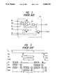
- FIG. 1 shows an example of the sequential logic circuit in which a logic circuit part 10 having an intended function is added with a scan circuit 20 for testing use, based on the conventional scan design system.
- the logic circuit part 10 is shown to be divided into a combinational circuit 12 and a flip-flop group 11 composed of a plurality of flip-flops FC for the sake of convenience.
- the scan circuit 20 is made up of a write circuit 21 and a specify circuit 22. Based on decoded addresses X and Y obtained by decoding a scan address (AxAy) with an X decoder 21x and a Y decoder 21y, the specify circuit 22 selectively specifies one of flip-flop circuits FC in the flip-flop group 11.
- each flip-flop circuit FC has such a construction as shown in FIG. 2, for example.
- a system clock Csy and a clear signal CL can be provided in common to all of the flip-flop circuits FC.
- input data di from the combinational circuit 12 is loaded by the system clock Csy into a flip-flop FF via a gate G2 and its output data do is applied to the combinational circuit 12.
- This construction is to implement the intended function of the logic circuit part 10.
- each flip-flop circuit FC includes gates G1 and G3, which are enabled by the decoded addresses X and Y which are provided from the specify circuit 22 for selecting the flip-flop circuit FC.
- a scan set signal Ss from the write circuit 21 is provided via the gate G1 of the selected flip-flop circuit FC to the flip-flop FF to set it.
- the output logic state of the flip-flop FF of the selected flip-flop circuit FC can be directly taken out of the logic circuit part 10, as a scan out signal Sout, via the gate G3.
- the output logic state of this flip-flop FF will also be referred to as the output logic state of the flip-flop circuit FC.
- the scan circuit 20 In the normal operation of the logic circuit part 10 as an ordinary logic circuit the scan circuit 20 is inoperative and the logic circuit part 10 performs the intended logical operation based on a system input data Din and the system clock Csy and provides system output data Dout.
- the testing of the logic circuit part 10 starts with initializing the flip-flop FF of every flip-flop circuit FC in the flip-flop group 11 to a "0" by the clear signal CL as shown in FIG. 3.
- a series of scan addresses (AxAy) for specifying flip-flops FF to be set to a "1" in the period T 1 are sequentially applied to the specify circuit 22 and, at the same time, a scan-in signal Sin and a scan clock Csc are applied to the write circuit 21, by which scan set signals Ss are sequentially provided to the flip-flop circuits FC specified by the scan addresses AxAy.
- predetermined system input data Din is applied to the logic circuit part 10 and, at the same time, one system clock Csy is provided, by which a transition is made in the internal state of the logic circuit part 10.
- a series of scan addresses (AxAy) for specifying the flip-flops FF are sequentially applied to the specify circuit 22 in period T 2 and output logic states of the specified flip-flops FF are sequentially read out as scan-out signals Sout.
- the system output data Dout after the state transition is also obtained.
- the clear signal CL is applied again to all the flip-flop circuits FC to initialize them and then the application of the scan set signal Ss to the flip-flop circuits FC, the transition of the internal state of the logic circuit part 10 by the system clock Csy and the readout of the scan-out signal Sout are repeated in the same manner as described above.
- the conventional circuit arrangement calls for inputting the clear signal CL prior to the setting by the scan circuit 20, and consequently, those of the flip-flops FF which have already been set and need not be reset will also be reset by the clear signal CL.
- the states of all the flip-flops FF in the flip-flop group 11 must be set again --this inevitably increases the time T 1 for setting the flip-flops FF.
- the sequential logic circuit device includes: a combinational circuit; a logic circuit part provided with a flip-flop group; a specify circuit for specifying each flip-flop in the flip-flop group directly from an external terminal; write means for arbitrarily writing a "0" or "1" into each flip-flop of the flip-flop group; and readout means for outputting the state of each flip-flop of the flip-flop group to an external terminal.
- FIG. 1 is a block diagram for explaining a conventional sequential logic circuit device
- FIG. 2 is a connection diagram for explaining the concrete structure of a flip-flop circuit for use in the device depicted in FIG. 1;
- FIG. 3 is timing chart for explaining the operation of the device shown in FIG. 1;
- FIG. 4 is a block diagram illustrating an embodiment of the sequential logic circuit device of the present invention.
- FIG. 5 is a connection diagram showing an example of the concrete structure of the flip-flop circuit for use in the embodiment of FIG. 4;
- FIG. 6 is a timing chart for explaining the operation of the device illustrated in FIG. 4.
- FIG. 4 illustrates the construction of the sequential logic circuit device according to the present invention.
- This embodiment is identical with the prior art example of FIG. 1 in the provision of the combinational circuit 12 and the flip-flop group 11 in the logic circuit part 10 and the scan circuit 20 but differs from the prior art in the constructions of each flip-flop circuit FC forming the flip-flop group 11 and the write circuit 21 forming the scan circuit 20 as described below.
- the write circuit 21 which forms the scan circuit 20 is constructed so that it can freely set a "0" or "1" in a desired one or ones of the flip-flops in the flip-flop group 11.
- the write circuit 21 is made up of two AND gates 21A and 21B and an inverter 21C and the scan-in signal Sin is applied to the one input terminal of the gate 21B and via the inverter 21C to the one input terminal of the gate 21A.
- the scan clock Csc is provided to the other input terminals of the gates 21A and 21B.
- the scan clock Csc is provided, as the scan set signal Ss, via the gate 21B to all of the flip-flop circuits FC in the flip-flop group 11, and a "1" is written into that one of the flip-flop circuits FC which is being specified by the specify circuit 22 at this time.
- the gate 21B When the scan-in signal Sin is switched to a "0", the gate 21B is disabled but instead the gate 21A is enabled. Consequently, in this instance the scan clock Csc is provided, as a scan reset signal Rs, via the gate 21A to all the flip-flop circuits FC in the flip-flop group 11, and a "0" is written into that one of the flip-flop circuits FC which is being specified by the specify circuit 22 at this time.
- FIG. 5 illustrates the construction of each flip-flop circuit FC which is provided in the flip-flop group 11.
- the flip-flop circuit FC is shown to be composed of a D type flip-flop DFF provided with a set input terminal S and a reset input terminal R, three AND gates G1, G2 and G3 which are enabled when the decoded addresses X and Y both match a "1", that is, when the flip-flop circuit FC is specified by the specify circuit 2, and one OR gate OR.
- the gate G1 is enabled when the decoded addresses X and Y both go to a "1", and if the scan set signal Ss mentioned above in respect of FIG. 4 is input at this time, it is provided to the set input terminal S of the D type flip-flop DFF, by which the flip-flop DFF is set and a "1" is written thereinto.
- the scan reset signal Rs is input into the gate G2 when the decoded addresses X and Y are both at the "1" level, the scan reset signal Rs is applied to the reset terminal R of the D type flip-flop DFF via the gate G2 and the OR gate OR, by which the D type flip-flop DFF is reset and a "0" is written thereinto.
- whether the scan set signal Ss or the scan reset signal Rs is input as mentioned above is dependent on whether the scan-in signal Sin which is provided to the write circuit 21 is a "1" or "0".
- the output logic state (a Q output) of the D type flip-flop DFF is directly output, as the scan-out signal Sout, to the outside of the logic circuit part 10. Since the gates G1 and G2 are also enabled together with the gate G3, the result of the write (set or reset) in the D flip-flop DFF can be read out at the same time as the write is effected in the flip-flop DFF, and the logic state of a desired one of the flip-flops can also be read out.
- the first step is to initialize the flip-flops DFF of all the flip-flop circuits FC in the flip-flop group 11 to the "0" level by the clear signal CL as shown in FIG. 6.
- a sequence of scan addresses (AxAy) for specifying the flip-flops DFF in which a "1" is to be set in the period T 1 are sequentially applied to the specify circuit 22 from the outside, and at the same time, the scan-in signal Sin and the scan clock Csc are provided to the write circuit 21, by which the scan set signal Ss or scan reset signal Rs is applied to the flip-flop circuit FC specified by the scan address (AxAy).
Landscapes
- Engineering & Computer Science (AREA)
- Physics & Mathematics (AREA)
- General Physics & Mathematics (AREA)
- General Engineering & Computer Science (AREA)
- Automation & Control Theory (AREA)
- Power Engineering (AREA)
- Computer Hardware Design (AREA)
- Computing Systems (AREA)
- Mathematical Physics (AREA)
- Tests Of Electronic Circuits (AREA)
- Test And Diagnosis Of Digital Computers (AREA)
- Electronic Switches (AREA)
Applications Claiming Priority (2)
| Application Number | Priority Date | Filing Date | Title |
|---|---|---|---|
| JP2059646A JPH03260739A (ja) | 1990-03-09 | 1990-03-09 | 順序動作型論理回路 |
| JP59646/90 | 1990-03-09 |
Publications (1)
| Publication Number | Publication Date |
|---|---|
| US5140176A true US5140176A (en) | 1992-08-18 |
Family
ID=13119186
Family Applications (1)
| Application Number | Title | Priority Date | Filing Date |
|---|---|---|---|
| US07/666,001 Expired - Fee Related US5140176A (en) | 1990-03-09 | 1991-03-07 | Sequential logic circuit device |
Country Status (5)
| Country | Link |
|---|---|
| US (1) | US5140176A (ja) |
| EP (1) | EP0445826B1 (ja) |
| JP (1) | JPH03260739A (ja) |
| KR (1) | KR940003081B1 (ja) |
| DE (1) | DE69114547T2 (ja) |
Cited By (8)
| Publication number | Priority date | Publication date | Assignee | Title |
|---|---|---|---|---|
| US5357144A (en) * | 1992-01-17 | 1994-10-18 | Sony Corporation | Complementary logic circuit |
| US5416362A (en) * | 1993-09-10 | 1995-05-16 | Unisys Corporation | Transparent flip-flop |
| US6645368B1 (en) | 1997-12-22 | 2003-11-11 | Roche Diagnostics Corporation | Meter and method of using the meter for determining the concentration of a component of a fluid |
| US20090068754A1 (en) * | 2006-10-24 | 2009-03-12 | Bayer Healthcare Llc | Transient Decay Amperometry |
| US8404100B2 (en) | 2005-09-30 | 2013-03-26 | Bayer Healthcare Llc | Gated voltammetry |
| US8425757B2 (en) | 2005-07-20 | 2013-04-23 | Bayer Healthcare Llc | Gated amperometry |
| US9410917B2 (en) | 2004-02-06 | 2016-08-09 | Ascensia Diabetes Care Holdings Ag | Method of using a biosensor |
| US9933385B2 (en) | 2007-12-10 | 2018-04-03 | Ascensia Diabetes Care Holdings Ag | Method of using an electrochemical test sensor |
Families Citing this family (3)
| Publication number | Priority date | Publication date | Assignee | Title |
|---|---|---|---|---|
| DE69317221T2 (de) * | 1992-11-24 | 1998-10-01 | Advanced Micro Devices Inc | Abtastprüfung für integrierte Schaltungen |
| US7494816B2 (en) | 1997-12-22 | 2009-02-24 | Roche Diagnostic Operations, Inc. | System and method for determining a temperature during analyte measurement |
| IT1303240B1 (it) * | 1998-08-07 | 2000-11-02 | Ansaldo Segnalamento Ferroviario Spa | Dispositivo e metodo di telecomando. |
Citations (5)
| Publication number | Priority date | Publication date | Assignee | Title |
|---|---|---|---|---|
| US4424581A (en) * | 1980-11-25 | 1984-01-03 | Nippon Electric Co., Ltd. | Logic circuit with a test capability |
| US4540903A (en) * | 1983-10-17 | 1985-09-10 | Storage Technology Partners | Scannable asynchronous/synchronous CMOS latch |
| US4580066A (en) * | 1984-03-22 | 1986-04-01 | Sperry Corporation | Fast scan/set testable latch using two levels of series gating with two current sources |
| US4970417A (en) * | 1988-07-07 | 1990-11-13 | Fujitsu Limited | Emitter coupled logic latch circuit |
| US5003204A (en) * | 1989-12-19 | 1991-03-26 | Bull Hn Information Systems Inc. | Edge triggered D-type flip-flop scan latch cell with recirculation capability |
Family Cites Families (2)
| Publication number | Priority date | Publication date | Assignee | Title |
|---|---|---|---|---|
| JPS51147937A (en) * | 1975-06-14 | 1976-12-18 | Fujitsu Ltd | Logic circuit device |
| AU3230084A (en) * | 1983-08-29 | 1985-03-07 | Amdahl Corporation | Serial chip scan |
-
1990
- 1990-03-09 JP JP2059646A patent/JPH03260739A/ja active Pending
-
1991
- 1991-03-04 KR KR1019910003485A patent/KR940003081B1/ko not_active Expired - Fee Related
- 1991-03-07 US US07/666,001 patent/US5140176A/en not_active Expired - Fee Related
- 1991-03-07 DE DE69114547T patent/DE69114547T2/de not_active Expired - Fee Related
- 1991-03-07 EP EP91103522A patent/EP0445826B1/en not_active Expired - Lifetime
Patent Citations (5)
| Publication number | Priority date | Publication date | Assignee | Title |
|---|---|---|---|---|
| US4424581A (en) * | 1980-11-25 | 1984-01-03 | Nippon Electric Co., Ltd. | Logic circuit with a test capability |
| US4540903A (en) * | 1983-10-17 | 1985-09-10 | Storage Technology Partners | Scannable asynchronous/synchronous CMOS latch |
| US4580066A (en) * | 1984-03-22 | 1986-04-01 | Sperry Corporation | Fast scan/set testable latch using two levels of series gating with two current sources |
| US4970417A (en) * | 1988-07-07 | 1990-11-13 | Fujitsu Limited | Emitter coupled logic latch circuit |
| US5003204A (en) * | 1989-12-19 | 1991-03-26 | Bull Hn Information Systems Inc. | Edge triggered D-type flip-flop scan latch cell with recirculation capability |
Cited By (21)
| Publication number | Priority date | Publication date | Assignee | Title |
|---|---|---|---|---|
| US5357144A (en) * | 1992-01-17 | 1994-10-18 | Sony Corporation | Complementary logic circuit |
| US5416362A (en) * | 1993-09-10 | 1995-05-16 | Unisys Corporation | Transparent flip-flop |
| US6645368B1 (en) | 1997-12-22 | 2003-11-11 | Roche Diagnostics Corporation | Meter and method of using the meter for determining the concentration of a component of a fluid |
| US10067082B2 (en) | 2004-02-06 | 2018-09-04 | Ascensia Diabetes Care Holdings Ag | Biosensor for determining an analyte concentration |
| US9410917B2 (en) | 2004-02-06 | 2016-08-09 | Ascensia Diabetes Care Holdings Ag | Method of using a biosensor |
| US8877035B2 (en) | 2005-07-20 | 2014-11-04 | Bayer Healthcare Llc | Gated amperometry methods |
| US8425757B2 (en) | 2005-07-20 | 2013-04-23 | Bayer Healthcare Llc | Gated amperometry |
| US8404100B2 (en) | 2005-09-30 | 2013-03-26 | Bayer Healthcare Llc | Gated voltammetry |
| US10670553B2 (en) | 2005-09-30 | 2020-06-02 | Ascensia Diabetes Care Holdings Ag | Devices using gated voltammetry methods |
| US11435312B2 (en) | 2005-09-30 | 2022-09-06 | Ascensia Diabetes Care Holdings Ag | Devices using gated voltammetry methods |
| US8647489B2 (en) | 2005-09-30 | 2014-02-11 | Bayer Healthcare Llc | Gated voltammetry devices |
| US9110013B2 (en) | 2005-09-30 | 2015-08-18 | Bayer Healthcare Llc | Gated voltammetry methods |
| US9835582B2 (en) | 2005-09-30 | 2017-12-05 | Ascensia Diabetes Care Holdings Ag | Devices using gated voltammetry methods |
| US8026104B2 (en) | 2006-10-24 | 2011-09-27 | Bayer Healthcare Llc | Transient decay amperometry |
| US20090068754A1 (en) * | 2006-10-24 | 2009-03-12 | Bayer Healthcare Llc | Transient Decay Amperometry |
| US10190150B2 (en) | 2006-10-24 | 2019-01-29 | Ascensia Diabetes Care Holdings Ag | Determining analyte concentration from variant concentration distribution in measurable species |
| US9005527B2 (en) | 2006-10-24 | 2015-04-14 | Bayer Healthcare Llc | Transient decay amperometry biosensors |
| US11091790B2 (en) | 2006-10-24 | 2021-08-17 | Ascensia Diabetes Care Holdings Ag | Determining analyte concentration from variant concentration distribution in measurable species |
| US8470604B2 (en) | 2006-10-24 | 2013-06-25 | Bayer Healthcare Llc | Transient decay amperometry |
| US9933385B2 (en) | 2007-12-10 | 2018-04-03 | Ascensia Diabetes Care Holdings Ag | Method of using an electrochemical test sensor |
| US10690614B2 (en) | 2007-12-10 | 2020-06-23 | Ascensia Diabetes Care Holdings Ag | Method of using an electrochemical test sensor |
Also Published As
| Publication number | Publication date |
|---|---|
| EP0445826B1 (en) | 1995-11-15 |
| EP0445826A2 (en) | 1991-09-11 |
| KR910017759A (ko) | 1991-11-05 |
| DE69114547D1 (de) | 1995-12-21 |
| EP0445826A3 (en) | 1991-10-23 |
| JPH03260739A (ja) | 1991-11-20 |
| DE69114547T2 (de) | 1996-05-02 |
| KR940003081B1 (ko) | 1994-04-13 |
Similar Documents
| Publication | Publication Date | Title |
|---|---|---|
| US3961252A (en) | Testing embedded arrays | |
| US6658611B1 (en) | Programmable built-in self-test system for semiconductor memory device | |
| US3961254A (en) | Testing embedded arrays | |
| USRE41496E1 (en) | Boundary-scan input circuit for a reset pin | |
| US4947395A (en) | Bus executed scan testing method and apparatus | |
| JPS6231439B2 (ja) | ||
| US4159541A (en) | Minimum pin memory device | |
| US6553530B1 (en) | Integrated circuit devices that include self-test apparatus for testing a plurality of functional blocks and methods of testing same | |
| JPH06500392A (ja) | 集積回路およびその集積回路をテストする方法 | |
| US5140176A (en) | Sequential logic circuit device | |
| KR0143361B1 (ko) | 복수의 시험 모드로 메모리 시험을 실행하는 반도체 메모리 장치 | |
| US4969126A (en) | Semiconductor memory device having serial addressing and operating method thereof | |
| US5425035A (en) | Enhanced data analyzer for use in bist circuitry | |
| US4802133A (en) | Logic circuit | |
| US5331644A (en) | Decoder checking circuits suitable for semiconductor memories | |
| JP2778443B2 (ja) | スキャンパステスト回路の最適化方法 | |
| US6463562B1 (en) | Semiconductor device including macros and its testing method | |
| US4873686A (en) | Test assist circuit for a semiconductor device providing fault isolation | |
| US6611929B1 (en) | Test circuit for memory | |
| US5844921A (en) | Method and apparatus for testing a hybrid circuit having macro and non-macro circuitry | |
| US4766593A (en) | Monolithically integrated testable registers that cannot be directly addressed | |
| US6219812B1 (en) | Apparatus and method for interfacing boundary-scan circuitry with DTL output drivers | |
| KR200195117Y1 (ko) | 스캔 플립플롭 회로 | |
| KR0129918Y1 (ko) | 셀프 테스트 기능을 갖는 메모리장치 | |
| KR100214315B1 (ko) | 에이직(asic) 내장 메모리의 성능검증회로 |
Legal Events
| Date | Code | Title | Description |
|---|---|---|---|
| AS | Assignment |
Owner name: ADVANTEST CORPORATION, 32-1, ASAHI-CHO 1-CHOME, NE Free format text: ASSIGNMENT OF ASSIGNORS INTEREST.;ASSIGNOR:OKINO, NOBORU;REEL/FRAME:005631/0941 Effective date: 19910302 |
|
| FEPP | Fee payment procedure |
Free format text: PAYOR NUMBER ASSIGNED (ORIGINAL EVENT CODE: ASPN); ENTITY STATUS OF PATENT OWNER: LARGE ENTITY |
|
| FPAY | Fee payment |
Year of fee payment: 4 |
|
| REMI | Maintenance fee reminder mailed | ||
| LAPS | Lapse for failure to pay maintenance fees | ||
| FP | Lapsed due to failure to pay maintenance fee |
Effective date: 20000818 |
|
| STCH | Information on status: patent discontinuation |
Free format text: PATENT EXPIRED DUE TO NONPAYMENT OF MAINTENANCE FEES UNDER 37 CFR 1.362 |