US5267045A - Multi-standard display device with scan conversion circuit - Google Patents
Multi-standard display device with scan conversion circuit Download PDFInfo
- Publication number
- US5267045A US5267045A US07/916,449 US91644992A US5267045A US 5267045 A US5267045 A US 5267045A US 91644992 A US91644992 A US 91644992A US 5267045 A US5267045 A US 5267045A
- Authority
- US
- United States
- Prior art keywords
- display device
- memory
- standard
- clock signal
- pictures
- Prior art date
- Legal status (The legal status is an assumption and is not a legal conclusion. Google has not performed a legal analysis and makes no representation as to the accuracy of the status listed.)
- Expired - Lifetime
Links
Images

Classifications
-
- H—ELECTRICITY
- H04—ELECTRIC COMMUNICATION TECHNIQUE
- H04N—PICTORIAL COMMUNICATION, e.g. TELEVISION
- H04N3/00—Scanning details of television systems; Combination thereof with generation of supply voltages
- H04N3/10—Scanning details of television systems; Combination thereof with generation of supply voltages by means not exclusively optical-mechanical
- H04N3/16—Scanning details of television systems; Combination thereof with generation of supply voltages by means not exclusively optical-mechanical by deflecting electron beam in cathode-ray tube, e.g. scanning corrections
- H04N3/27—Circuits special to multi-standard receivers
-
- H—ELECTRICITY
- H04—ELECTRIC COMMUNICATION TECHNIQUE
- H04N—PICTORIAL COMMUNICATION, e.g. TELEVISION
- H04N3/00—Scanning details of television systems; Combination thereof with generation of supply voltages
- H04N3/10—Scanning details of television systems; Combination thereof with generation of supply voltages by means not exclusively optical-mechanical
- H04N3/12—Scanning details of television systems; Combination thereof with generation of supply voltages by means not exclusively optical-mechanical by switched stationary formation of lamps, photocells or light relays
- H04N3/127—Scanning details of television systems; Combination thereof with generation of supply voltages by means not exclusively optical-mechanical by switched stationary formation of lamps, photocells or light relays using liquid crystals
Definitions
- the invention relates to a multi-standard display device for displaying pictures having a television-standard-dependent format, which device comprises a matrix display screen (such as a liquid-crystal display), a video signal processing circuit for receiving and processing the pictures, said pictures having a format-associated number of lines in a first direction, a sync separator for determining horizontal and vertical synchronizing signals and a standard-conversion circuit for converting the pictures of the television-standard-dependent format into pictures having a display screen-associated format.
- a matrix display screen such as a liquid-crystal display
- a video signal processing circuit for receiving and processing the pictures, said pictures having a format-associated number of lines in a first direction
- a sync separator for determining horizontal and vertical synchronizing signals
- a standard-conversion circuit for converting the pictures of the television-standard-dependent format into pictures having a display screen-associated format.
- a multi-standard display device of this type is known from European Patent Application EP-A-400286.
- a multi-standard display device is understood to mean a display device which is suitable for a plurality of television standards (PAL, NTSC, HDTV, etc.). Since a display device with a liquid crystal display screen (LCD) has a fixed number of display lines, the incoming video signal will have to be converted to a picture having a fixed number of display lines (viz. the number of display lines of the LCD screen) so as to ensure that the display device is suitable for, for example, both PAL (625 lines) and NTSC (525 lines).
- a drawback of this known multi-standard display device is that the vertical interpolation is complicated and hence costly. Each pixel of each interpositioned line must be computed.
- the multi-standard display device comprises a scan-conversion circuit for converting pictures having lines in the first direction into lines in a second direction perpendicular to the first direction, said second-direction lines being applied to the display screen and being displayed in the second direction under the control of a control circuit.
- a cathode ray tube (CRT) display device in which the lines are written vertically instead of horizontally is known from U.S. Pat. No. 4,989,092.
- the reason of displaying the lines vertically on a CRT display screen is that the deflection is effected at the fastest rate, (namely the line rate) into the direction having the smallest deflection angle and hence the smallest amplitude. Consequently, there is a considerable reduction of the energy dissipation. This aspect will become increasingly more important as display devices get bigger, and certainly also for 16:9 display devices.
- An embodiment of a multi-standard display device is characterized in that the scan-conversion circuit comprises a memory which reads in the pictures line by line in the first direction under the control of a first clock signal and reads them out in the direction perpendicular to the first direction under the control of a second clock signal.
- Reading in and reading out with (possibly) different clock signals provides the freedom of enlarging, for example, a part of the picture, which will often be necessary because the number of pixels per line and the number of lines of a picture are not equal.
- a further embodiment of a multi-standard display device is characterized in that the control circuit comprises a row driver and a column driver, said row driver receiving the video information in an analog form with lines in the second direction, a third clock signal controlling said row driver and a fourth clock signal controlling said column driver.
- the video information is applied to the column driver of the control circuit and by means of a clock signal it is determined at which instant the next line must be written on the liquid crystal display screen. Since in multi-standard display devices according to the invention the lines are read from the memory in a direction perpendicular to the read-in direction, it is advantageous to apply the video information to the row driver instead of to the column driver.
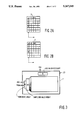
- FIG. 1 shows an embodiment of a multi-standard display device according to the invention
- FIGS. 2A and 2B show diagrammatically the way in which the memories according to the invention are read in and read out
- FIG. 3 shows the display screen with a row driver and a column driver.
- FIG. 1 shows an embodiment of a display device W in which the video signal, a horizontal synchronizing signal Hsync and a vertical synchronizing signal Vsync are received at inputs 1a, 1b and 1c, respectively.
- the input 1a is coupled to an A/D converter 2 which takes samples of the video signal under the control of a first clock signal ck1.
- the output signal of the A/D converter is applied to the master contact of a switch S1, a first switching contact a of which is connected to a memory 3.
- the samples of a first field of the video signal are stored in the memory 3 (see the dashed line in FIG. 2A) under the control of clock signals.
- the memory has an internal structure of a matrix and is filled row by row with video information.
- the clock signal ck1 determines the allocation of memory elements in a row, while a clock signal ck5 determines the row drive of the memory.
- the switch S1 is changed over (from switching contact a to switching contact b) and the second field is read row by row into a memory 4 (see the dot-dash line in FIG. 2B).
- the memory 4 is also controlled by clock signals, the clock signal ck1 again determining the allocation of the memory elements in a row and the clock signal ck5 determining the row drive.
- the video information stored in the memory 3 is vertically read out of the memory 3 (see the dot-dash line in FIG. 2A) under the control of clock signals ck2 and ck6 via a switch S2, a switching contact c of which is coupled to the memory during this field.
- the clock signal ck2 determines the allocation of the memory elements in a column and the clock signal ck6 determines the column drive.
- the master contact of the switch S2 is connected to a D/A converter 5 which converts the (digital) samples into an analog signal under the control of the clock signal ck2. This analog signal is subsequently applied to the drive unit of the LCD screen 7 via a low-pass filter 6.
- the drive unit of the LCD screen comprises a row drive circuit A (see FIG. 3), which receives the analog video signal and takes samples of the video signal under the control of a clock signal ck3. Each sample is applied to a sample-and-hold circuit SH (see FIG. 3). After all elements of a column have been applied to a sample-and-hold circuit, the column is written as a whole on the LCD screen under the control of a column drive circuit B (see FIG. 3). A clock signal ck4 defines the instant when the relevant column is written.
- the switches S1 and S2 and the memories 3 and 4 jointly constitute a scan-conversion circuit AOS.
- This scan-conversion circuit reads in the video information horizontally and line by line (row by row) and reads out the video information vertically and column by column.
- the inputs 1b and 1c of the display device are coupled to a clock generator 8.
- the clock generator defines the format of the video signal and thus the required values of the clock signals ck1, ck2, ck3, ck4, ck5 and ck6 for reading the video information into the memories in the correct manner and for subsequently reading it out of the memories again and for displaying it on the LCD screen.
- the horizontal synchronizing signal indicates whether the incoming video signal has 625 lines, 525 lines, 1250 lines or a different line number.
- the vertical synchronizing signal indicates whether the incoming video signal has a picture frequency of 50 Hz, 60 Hz, 100 Hz or a different picture frequency. Together, these synchronizing signals indicate whether the video information comprises pictures in accordance with the PAL, NTSC or HDTV standard or a different standard.
- the required number of rows of the memories is equal to the number of effective lines to be displayed of a field of the incoming video signal.
- the required number of columns of the memories is equal to the number of columns of the LCD display screen.
- the width of the picture can be varied by varying the sampling frequency, the starting moment and the sampling period of the clock signal ck1 during reading into the memories.
- the height of the picture can be varied by varying the frequency of the clock signal ck2 for reading out the memories and by varying the first position which is read out. For example, when a 9:16 display screen is used, a 3:4 video signal can be enlarged to a 9:16 picture, in which the upper and lower parts of the picture are lost, however. Moreover, 3:4 pictures of cinematographic picture format with a black bar at the upper and lower sides can be enlarged to a full 9:16 picture.
- the A/D converter and the D/A converter may be dispensed with because the video information is stored in the form of charges on capacitors in a CCD.
- a part of the picture can be enlarged ("zoom") by firstly increasing the frequency of the read clock ck1 during reading into the memory and, secondly, by increasing the sampling frequency ck3 at the display screen.
- each video line is presented as a whole to the column (video) driver. These lines are then written one by one into the display under the control of the row selection driver. The video information is then vertically read out of the memory.
- the number of rows and columns of the LCD display screen is optional. These numbers are not bound to any television standard.
- the number of pixels of the LCD screen can be chosen on the basis of invisibility of individual pixels and need not be chosen on the basis of a television standard.
- the frequencies of the different clock signals do not need to have a strict relationship with the incoming video information.
- the field frequency is chosen to be equal to the field frequency of the incoming video information.
- the frequencies of the clock signals should only be chosen in such a way that all pixels in each field are provided with new information. Missing lines (due to interlacing) are interpolated in known manner.
- the video information is applied to the input 1a in the form of RGB signals or in the form of YUV signals.
Landscapes
- Engineering & Computer Science (AREA)
- Multimedia (AREA)
- Signal Processing (AREA)
- Chemical & Material Sciences (AREA)
- Crystallography & Structural Chemistry (AREA)
- Transforming Electric Information Into Light Information (AREA)
- Liquid Crystal Display Device Control (AREA)
- Color Television Systems (AREA)
Applications Claiming Priority (2)
| Application Number | Priority Date | Filing Date | Title |
|---|---|---|---|
| EP91201900 | 1991-07-19 | ||
| EP91201900.7 | 1991-07-19 |
Publications (1)
| Publication Number | Publication Date |
|---|---|
| US5267045A true US5267045A (en) | 1993-11-30 |
Family
ID=8207792
Family Applications (1)
| Application Number | Title | Priority Date | Filing Date |
|---|---|---|---|
| US07/916,449 Expired - Lifetime US5267045A (en) | 1991-07-19 | 1992-07-17 | Multi-standard display device with scan conversion circuit |
Country Status (4)
| Country | Link |
|---|---|
| US (1) | US5267045A (fr) |
| EP (1) | EP0523792B1 (fr) |
| JP (1) | JP3335195B2 (fr) |
| DE (1) | DE69212076T2 (fr) |
Cited By (21)
| Publication number | Priority date | Publication date | Assignee | Title |
|---|---|---|---|---|
| US5489952A (en) * | 1993-07-14 | 1996-02-06 | Texas Instruments Incorporated | Method and device for multi-format television |
| WO1997035294A1 (fr) * | 1996-03-18 | 1997-09-25 | Philips Electronics N.V. | Affichage adresse par plasma |
| US5956082A (en) * | 1995-02-24 | 1999-09-21 | Canon Kabushiki Kaisha | Video signal processing apparatus |
| US5982443A (en) * | 1997-04-19 | 1999-11-09 | Hyundai Electronics Industries Co., Ltd. | Apparatus and method for converting scan format of video signal |
| US6005990A (en) * | 1996-06-10 | 1999-12-21 | International Business Machines Corporation | System for optically scanning images using optical shutter |
| US6118429A (en) * | 1993-09-30 | 2000-09-12 | Hitachi, Ltd. | Liquid crystal display system capable of reducing and enlarging resolution of input display data |
| US6121941A (en) * | 1991-09-05 | 2000-09-19 | Deutsche Thomson-Brandt Gmbh | Method and device for the controlling of matrix displays |
| US6429899B1 (en) * | 1998-07-16 | 2002-08-06 | Matsushita Electric Industrial Co., Ltd. | Video display apparatus with scan conversion and reversion and a video display method using scan conversion and reversion |
| US6542150B1 (en) | 1996-06-28 | 2003-04-01 | Cirrus Logic, Inc. | Method and apparatus for asynchronous display of graphic images |
| US6751001B1 (en) | 2003-01-24 | 2004-06-15 | Evans & Sutherland Computer Corporation | Non-sampled auto-format conversion method |
| US20040145708A1 (en) * | 2003-01-24 | 2004-07-29 | Evans & Sutherland Computer Corporation | Infrared projector |
| US20050174071A1 (en) * | 2002-04-04 | 2005-08-11 | Simpson Theodore F. | Transposed bi-directional scanning in a cathode ray tube |
| US20060103679A1 (en) * | 2004-11-16 | 2006-05-18 | Samsung Electro-Mechanics Co., Ltd. | Apparatus and method for transposing data |
| US20060221247A1 (en) * | 2005-03-31 | 2006-10-05 | Didier Doyen | Vertical scanning television |
| US20080034171A1 (en) * | 2006-07-28 | 2008-02-07 | Taejoong Song | Systems, Methods, and Apparatuses for Digital Wavelet Generators for Multi-Resolution Spectrum Sensing of Cognitive Radio Applications |
| US7891818B2 (en) | 2006-12-12 | 2011-02-22 | Evans & Sutherland Computer Corporation | System and method for aligning RGB light in a single modulator projector |
| US20110166968A1 (en) * | 2010-01-06 | 2011-07-07 | Richard Yin-Ching Houng | System and method for activating display device feature |
| US8077378B1 (en) | 2008-11-12 | 2011-12-13 | Evans & Sutherland Computer Corporation | Calibration system and method for light modulation device |
| US8358317B2 (en) | 2008-05-23 | 2013-01-22 | Evans & Sutherland Computer Corporation | System and method for displaying a planar image on a curved surface |
| US8702248B1 (en) | 2008-06-11 | 2014-04-22 | Evans & Sutherland Computer Corporation | Projection method for reducing interpixel gaps on a viewing surface |
| US9641826B1 (en) | 2011-10-06 | 2017-05-02 | Evans & Sutherland Computer Corporation | System and method for displaying distant 3-D stereo on a dome surface |
Families Citing this family (4)
| Publication number | Priority date | Publication date | Assignee | Title |
|---|---|---|---|---|
| EP0710019A3 (fr) * | 1994-10-31 | 1997-03-26 | Texas Instruments Inc | Dispositif d'affichage numérique à micro-mirroirs pour la télévision |
| JP4608761B2 (ja) * | 2000-10-27 | 2011-01-12 | ソニー株式会社 | 映像信号処理装置及び方法 |
| WO2006073792A1 (fr) * | 2004-12-31 | 2006-07-13 | Thomson Licensing | Ecran cathodique a balayage vertical multistandard |
| CN116546333B (zh) * | 2023-04-03 | 2023-10-31 | 华光影像科技合肥有限公司 | 同时输出不同拍摄模式的视频画面的方法、系统和摄像机 |
Citations (5)
| Publication number | Priority date | Publication date | Assignee | Title |
|---|---|---|---|---|
| US3342937A (en) * | 1962-08-01 | 1967-09-19 | Battelle Development Corp | Synchronizing of electron beam scanning in a narrow bandwidth pseudorandom dot scan television system |
| US4694348A (en) * | 1985-06-14 | 1987-09-15 | Citizen Watch Co., Ltd. | Method of driving liquid crystal display panel of TV receiver |
| EP0400286A2 (fr) * | 1989-06-02 | 1990-12-05 | GRUNDIG E.M.V. Elektro-Mechanische Versuchsanstalt Max Grundig holländ. Stiftung & Co. KG. | Circuit de conversion de standards de signaux vidéo pour la représentation sur un appareil de reproduction comportant un dispositif d'affichage matriciel |
| US4989092A (en) * | 1988-12-07 | 1991-01-29 | U.S. Philips Corporation | Picture display device using scan direction transposition |
| US5091784A (en) * | 1989-09-07 | 1992-02-25 | Hitachi, Ltd. | Matrix type image display apparatus using non-interlace scanning system |
Family Cites Families (2)
| Publication number | Priority date | Publication date | Assignee | Title |
|---|---|---|---|---|
| NL8501582A (nl) | 1985-02-12 | 1986-09-01 | Philips Nv | Videosignaalverwerkingsschakeling voor de verwerking van een geinterlinieerd videosignaal. |
| JPH084340B2 (ja) * | 1985-08-07 | 1996-01-17 | セイコーエプソン株式会社 | インタ−フエイス装置 |
-
1992
- 1992-07-10 EP EP92202101A patent/EP0523792B1/fr not_active Expired - Lifetime
- 1992-07-10 DE DE69212076T patent/DE69212076T2/de not_active Expired - Lifetime
- 1992-07-17 US US07/916,449 patent/US5267045A/en not_active Expired - Lifetime
- 1992-07-17 JP JP19095292A patent/JP3335195B2/ja not_active Expired - Lifetime
Patent Citations (5)
| Publication number | Priority date | Publication date | Assignee | Title |
|---|---|---|---|---|
| US3342937A (en) * | 1962-08-01 | 1967-09-19 | Battelle Development Corp | Synchronizing of electron beam scanning in a narrow bandwidth pseudorandom dot scan television system |
| US4694348A (en) * | 1985-06-14 | 1987-09-15 | Citizen Watch Co., Ltd. | Method of driving liquid crystal display panel of TV receiver |
| US4989092A (en) * | 1988-12-07 | 1991-01-29 | U.S. Philips Corporation | Picture display device using scan direction transposition |
| EP0400286A2 (fr) * | 1989-06-02 | 1990-12-05 | GRUNDIG E.M.V. Elektro-Mechanische Versuchsanstalt Max Grundig holländ. Stiftung & Co. KG. | Circuit de conversion de standards de signaux vidéo pour la représentation sur un appareil de reproduction comportant un dispositif d'affichage matriciel |
| US5091784A (en) * | 1989-09-07 | 1992-02-25 | Hitachi, Ltd. | Matrix type image display apparatus using non-interlace scanning system |
Cited By (31)
| Publication number | Priority date | Publication date | Assignee | Title |
|---|---|---|---|---|
| US6121941A (en) * | 1991-09-05 | 2000-09-19 | Deutsche Thomson-Brandt Gmbh | Method and device for the controlling of matrix displays |
| US5489952A (en) * | 1993-07-14 | 1996-02-06 | Texas Instruments Incorporated | Method and device for multi-format television |
| US6310602B1 (en) | 1993-09-30 | 2001-10-30 | Hitachi, Ltd. | Liquid crystal display system capable of reducing and enlarging resolution of input display data |
| US6587120B2 (en) | 1993-09-30 | 2003-07-01 | Hitachi, Ltd. | Liquid crystal display system capable of reducing and enlarging resolution of input display data |
| US6118429A (en) * | 1993-09-30 | 2000-09-12 | Hitachi, Ltd. | Liquid crystal display system capable of reducing and enlarging resolution of input display data |
| US5956082A (en) * | 1995-02-24 | 1999-09-21 | Canon Kabushiki Kaisha | Video signal processing apparatus |
| WO1997035294A1 (fr) * | 1996-03-18 | 1997-09-25 | Philips Electronics N.V. | Affichage adresse par plasma |
| US6130655A (en) * | 1996-03-18 | 2000-10-10 | U.S. Philips Corporation | Plasma-addressed display |
| US6005990A (en) * | 1996-06-10 | 1999-12-21 | International Business Machines Corporation | System for optically scanning images using optical shutter |
| US6542150B1 (en) | 1996-06-28 | 2003-04-01 | Cirrus Logic, Inc. | Method and apparatus for asynchronous display of graphic images |
| US7209133B2 (en) | 1996-06-28 | 2007-04-24 | Nvidia International, Inc. | Method and apparatus for asynchronous display of graphic images |
| US20030227471A1 (en) * | 1996-06-28 | 2003-12-11 | Eglit Alexander J. | Method and apparatus for asynchronous display of graphic images |
| US20030234801A1 (en) * | 1996-06-28 | 2003-12-25 | Eglit Alexander J. | Method and apparatus for asynchronous display of graphic images |
| US7623126B2 (en) | 1996-06-28 | 2009-11-24 | Nvidia Corporation | Method and apparatus for asynchronous display of graphic images |
| US5982443A (en) * | 1997-04-19 | 1999-11-09 | Hyundai Electronics Industries Co., Ltd. | Apparatus and method for converting scan format of video signal |
| US6429899B1 (en) * | 1998-07-16 | 2002-08-06 | Matsushita Electric Industrial Co., Ltd. | Video display apparatus with scan conversion and reversion and a video display method using scan conversion and reversion |
| US20050174071A1 (en) * | 2002-04-04 | 2005-08-11 | Simpson Theodore F. | Transposed bi-directional scanning in a cathode ray tube |
| US6751001B1 (en) | 2003-01-24 | 2004-06-15 | Evans & Sutherland Computer Corporation | Non-sampled auto-format conversion method |
| US20040145708A1 (en) * | 2003-01-24 | 2004-07-29 | Evans & Sutherland Computer Corporation | Infrared projector |
| US20060103679A1 (en) * | 2004-11-16 | 2006-05-18 | Samsung Electro-Mechanics Co., Ltd. | Apparatus and method for transposing data |
| US7411630B2 (en) * | 2004-11-16 | 2008-08-12 | Samsung Electro-Mechanics Co., Ltd. | Apparatus and method for transposing data in the display system using the optical modulator |
| US20060221247A1 (en) * | 2005-03-31 | 2006-10-05 | Didier Doyen | Vertical scanning television |
| US20080034171A1 (en) * | 2006-07-28 | 2008-02-07 | Taejoong Song | Systems, Methods, and Apparatuses for Digital Wavelet Generators for Multi-Resolution Spectrum Sensing of Cognitive Radio Applications |
| US7482962B2 (en) * | 2006-07-28 | 2009-01-27 | Samsung Electro-Mechanics | Systems, methods, and apparatuses for digital wavelet generators for Multi-Resolution Spectrum Sensing of Cognitive Radio applications |
| US7891818B2 (en) | 2006-12-12 | 2011-02-22 | Evans & Sutherland Computer Corporation | System and method for aligning RGB light in a single modulator projector |
| US8358317B2 (en) | 2008-05-23 | 2013-01-22 | Evans & Sutherland Computer Corporation | System and method for displaying a planar image on a curved surface |
| US8702248B1 (en) | 2008-06-11 | 2014-04-22 | Evans & Sutherland Computer Corporation | Projection method for reducing interpixel gaps on a viewing surface |
| US8077378B1 (en) | 2008-11-12 | 2011-12-13 | Evans & Sutherland Computer Corporation | Calibration system and method for light modulation device |
| US20110166968A1 (en) * | 2010-01-06 | 2011-07-07 | Richard Yin-Ching Houng | System and method for activating display device feature |
| US9641826B1 (en) | 2011-10-06 | 2017-05-02 | Evans & Sutherland Computer Corporation | System and method for displaying distant 3-D stereo on a dome surface |
| US10110876B1 (en) | 2011-10-06 | 2018-10-23 | Evans & Sutherland Computer Corporation | System and method for displaying images in 3-D stereo |
Also Published As
| Publication number | Publication date |
|---|---|
| EP0523792A3 (en) | 1993-06-09 |
| DE69212076T2 (de) | 1997-01-30 |
| JP3335195B2 (ja) | 2002-10-15 |
| EP0523792B1 (fr) | 1996-07-10 |
| JPH05207477A (ja) | 1993-08-13 |
| DE69212076D1 (de) | 1996-08-14 |
| EP0523792A2 (fr) | 1993-01-20 |
Similar Documents
| Publication | Publication Date | Title |
|---|---|---|
| US5267045A (en) | Multi-standard display device with scan conversion circuit | |
| KR0148015B1 (ko) | 픽쳐-인-픽쳐 텔레비젼 시스템 | |
| US4953025A (en) | Apparatus for defining an effective picture area of a high definition video signal when displayed on a screen with a different aspect ratio | |
| US4364090A (en) | Method for a compatible increase in resolution in television systems | |
| KR100186409B1 (ko) | 피씨와 티브이 적응형 피아이피 영상신호 처리회로 | |
| KR950014577B1 (ko) | 고화질 텔레비젼의 픽쳐인픽쳐신호처리방법 및 그 장치 | |
| US6480230B1 (en) | Image processing of video signal for display | |
| US5396290A (en) | Apparatus and method for controlling a high resolution charge coupled device image sensor to provide alternative modes of picture imaging | |
| US5021887A (en) | Method and circuit for composing still image of picture-in-picture | |
| KR0182930B1 (ko) | 디스플레이 장치의 주사 방식 변환 장치 및 변환방법 | |
| US5999227A (en) | Special features for digital television | |
| JPH0247918B2 (fr) | ||
| US5173777A (en) | Circuit configuration for inset-image keying in a television set having only one tuner | |
| US5321509A (en) | Apparatus and method for controlling a charge coupled device image sensor to provide sequential output of video image signals | |
| JPS61193580A (ja) | 2画面テレビジヨン受像機 | |
| EP1506671B1 (fr) | Affichage video et texte | |
| JPH07162765A (ja) | 撮像装置及び表示装置 | |
| JPH11136592A (ja) | 画像処理装置 | |
| JP3469596B2 (ja) | マトリクス型表示装置 | |
| JPH05508287A (ja) | 共通ccdセンサを用いた2重規格カメラ | |
| KR0123769B1 (ko) | 16 : 9 화면에서의 픽쳐 인 픽쳐 표시회로 | |
| KR940007547B1 (ko) | 티브이 2화면 장치 | |
| JPS6345098Y2 (fr) | ||
| JP2911133B2 (ja) | ハイビジョン受信機の時間圧縮装置 | |
| JP2548017B2 (ja) | 倍速変換装置 |
Legal Events
| Date | Code | Title | Description |
|---|---|---|---|
| AS | Assignment |
Owner name: U.S. PHILIPS CORPORATION A CORP. OF DELAWARE, NE Free format text: ASSIGNMENT OF ASSIGNORS INTEREST.;ASSIGNOR:STROOMER, MARTINUS V.C.;REEL/FRAME:006227/0227 Effective date: 19920617 |
|
| STCF | Information on status: patent grant |
Free format text: PATENTED CASE |
|
| FPAY | Fee payment |
Year of fee payment: 4 |
|
| FPAY | Fee payment |
Year of fee payment: 8 |
|
| FPAY | Fee payment |
Year of fee payment: 12 |
|
| AS | Assignment |
Owner name: ADREA, LLC, CALIFORNIA Free format text: ASSIGNMENT OF ASSIGNORS INTEREST;ASSIGNORS:PHILIPS ELECTRONICS NORTH AMERICA CORPORATION;KONINKLIJKE PHILIPS ELECTRONICS N.V.;U.S. PHILIPS CORPORATION;REEL/FRAME:025679/0900 Effective date: 20101111 |