US5270876A - Apparatus for reproducing data recorded on a magnetic recording medium - Google Patents
Apparatus for reproducing data recorded on a magnetic recording medium Download PDFInfo
- Publication number
- US5270876A US5270876A US07/482,302 US48230290A US5270876A US 5270876 A US5270876 A US 5270876A US 48230290 A US48230290 A US 48230290A US 5270876 A US5270876 A US 5270876A
- Authority
- US
- United States
- Prior art keywords
- signal
- data
- decoding
- digital
- comparator
- Prior art date
- Legal status (The legal status is an assumption and is not a legal conclusion. Google has not performed a legal analysis and makes no representation as to the accuracy of the status listed.)
- Expired - Lifetime
Links
Images


Classifications
-
- H—ELECTRICITY
- H04—ELECTRIC COMMUNICATION TECHNIQUE
- H04N—PICTORIAL COMMUNICATION, e.g. TELEVISION
- H04N5/00—Details of television systems
- H04N5/76—Television signal recording
- H04N5/91—Television signal processing therefor
- H04N5/93—Regeneration of the television signal or of selected parts thereof
- H04N5/931—Regeneration of the television signal or of selected parts thereof for restoring the level of the reproduced signal
-
- G—PHYSICS
- G11—INFORMATION STORAGE
- G11B—INFORMATION STORAGE BASED ON RELATIVE MOVEMENT BETWEEN RECORD CARRIER AND TRANSDUCER
- G11B20/00—Signal processing not specific to the method of recording or reproducing; Circuits therefor
- G11B20/10—Digital recording or reproducing
- G11B20/10009—Improvement or modification of read or write signals
-
- G—PHYSICS
- G11—INFORMATION STORAGE
- G11B—INFORMATION STORAGE BASED ON RELATIVE MOVEMENT BETWEEN RECORD CARRIER AND TRANSDUCER
- G11B20/00—Signal processing not specific to the method of recording or reproducing; Circuits therefor
- G11B20/10—Digital recording or reproducing
- G11B20/10527—Audio or video recording; Data buffering arrangements
-
- H—ELECTRICITY
- H04—ELECTRIC COMMUNICATION TECHNIQUE
- H04N—PICTORIAL COMMUNICATION, e.g. TELEVISION
- H04N5/00—Details of television systems
- H04N5/76—Television signal recording
- H04N5/91—Television signal processing therefor
- H04N5/92—Transformation of the television signal for recording, e.g. modulation, frequency changing; Inverse transformation for playback
- H04N5/926—Transformation of the television signal for recording, e.g. modulation, frequency changing; Inverse transformation for playback by pulse code modulation
Definitions
- the present invention relates generally to a device for reproducing magnetically recorded data and more specifically is directed to an apparatus for reproducing video signals which have been digitized.
- the video signal is frequency modulated and then recorded as an analog signal on magnetic tape.
- the video signal is converted into a digital signal prior to recording, it is possible to repeatedly dub or copy the recorded signals without incurring any deterioration in the characteristics thereof.
- the magnetic head, the tape and the like of the electromagnetic transducing system exhibit characteristics which, in the low frequency and high frequency regions, cause reduction in the S/N ratio.
- a digitized video signal (hereinafter referred to as a digital signal) may be limited to a narrow frequency range. Therefore, it is necessary to use a recording system by which the frequency spectrum enables the S/N ratio to approach its maximum value.
- FIG. 19 A video recorder, which has been proposed in order to take advantage of the fact that digital video signals can be dubbed without undergoing any deterioration, is shown on FIG. 19.
- predetermined recording data D REC is supplied via an amplifier 3 to a magnetic recording head 4 and recorded thereby on magnetic tape 5.
- a magnetic playback head 6 is used to reproduce a signal S RF which is supplied through an amplifier 8 and an equalizing circuit 9 to a decoding circuit 10.
- a clock signal Sck is produced by a clock signal generator 12 and supplied to the decoding circuit 10.
- the decoding circuit 10 responds thereto by checking the level of the reproduced signal S RF with respect to a predetermined reference value, at a predetermined timing, and outputting reproduction characteristic data D RB which is then used to decode the digitized video signal.
- a slice level value in the decoding circuit 10 may become variable and it then becomes necessary to prevent bit error from appearing in the reproduction characteristic data.
- an arrangement having a Viterbi decoding circuit in which, when data falls within a predetermined range, the level of the reproduced signal is sensed and the level of the reproduced signal is corrected in a manner which reduces bit error caused by noise in the reproduced signal.
- a device for reproducing magnetic recordings features means for recording data on a recording media and for obtaining a reproduced signal therefrom and means for correcting a previous input data value in response to change in an instant input data value.
- a system for recording and reproducing data comprises means for converting an input signal from analog form into digital data; a moving body on which the digital data can be recorded; means for reading the data recorded on the moving body and producing an analog playback signal indicative thereof; means for converting the analog playback signal into a digital playback signal; signal dividing means for separating the digital playback signal into first and second signal portions; first and second Viterbi decoding circuits which respectively receive the first and second signal portions; signal re-combining means for receiving the outputs of the first and second Viterbi decoding circuits and forming a reconstituted digital signal; means for converting the reconstituted digital into an analog output signal; and means associated with the first and second Viterbi decoding circuits for modifying either the output of, or the signal which is input to the first and second viterbi circuits to reduce the bit error in the output of the first and second Viterbi circuits.
- FIG. 1 is a block diagram showing a video tape recording device according to a first embodiment of the present invention
- FIGS. 2(A)-2(E) are timing charts showing the waveforms of various signals which are produced in the circuit arrangement shown in FIG. 1;
- FIG. 3 is a circuit diagram showing details of a precoding circuit used in the device of FIG. 1;
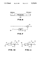
- FIG. 4 is a graph showing, in terms of S/N ratio and frequency, the frequency dependency of the reproduction characteristics
- FIG. 5 is a graph which demonstrates, in terms of response and frequency, the technique which underlies the Class IV partial response method
- FIG. 6 is a diagram showing the arrangement of data used in the device of FIG. 1;
- FIG. 7 is a block diagram showing details of a calculation processing circuit utilized in the device shown in FIG. 1;
- FIGS. 8 and 9 are diagrams which illustrate the operation of viterbi decoding circuits used in the embodiment of the present invention shown on FIG. 1;
- FIGS. 10 and 11 are block diagrams showing equivalence circuits used in electromagnetic recording/reproducing systems embodying this invention.
- FIG. 12 is a block diagram showing the arrangement of a Viterbi decoding circuit in the first embodiment of the present invention.
- FIGS. 13 to 18 are diagrams which illustrate operation of the Viterbi decoding circuit
- FIG. 19 is a block diagram showing the arrangement of a previously proposed video tape recorder arrangement
- FIG. 20 is a block diagram similar to that of FIG. 1, but showing another embodiment of the present invention.
- FIG. 21 is a block diagram similar to that of FIG. 12, but showing a circuit arrangement which characterizes the embodiment of FIG. 20.
- a recording and/or reproducing device 20 comprises a recording section having an A/D converter 22, a data compression circuit 24, an error correction circuit 26, a pre-coding circuit 28, an adder 29, an amplifier 30 and recording heads 4A and 4B which are serially connected.
- the device 20 further comprises a playback section which includes an amplifier 8, an equalizer circuit 9, a variable gain amplifier 31, a calculation processing circuit 32 and an A/D converter 37 which are also serially connected.
- a first selection or switching circuit 39 is connected to the output of the A/D converter 37 and is arranged to selectively switch between first and second Viterbi decoding circuits 40 and 41.
- the outputs of the Viterbi circuits 40 and 41 are connected with a second selection or switching circuit 80 which selectively channels data from the Viterbi circuits 40 and 41 to a series circuit of an error detection and correction circuit 81, a data expansion circuit 82 and a D/A converter 83.
- a comparator 70 has one of its three inputs connected to terminals of the Viterbi circuits 40 and 41 from which data ⁇ K are output. The other two inputs of the comparator 70 are connected to sources of reference voltages D REF1 and D REF2 , respectively.
- the output of the comparator 70 is connected to a switch circuit 71, which, as shown, is responsive to the output of the comparator 70 to selectively connect or disconnect an output of a D/A circuit 72 with respect to a gain-control input of the variable gain amplifier 31.
- the input of the D/A circuit 72 is connected with the output of the A/D converter 37.
- a sample and hold condenser 73 is connected between ground and the output terminal of the switch circuit 71.
- the A/D converter 22 receives an input video signal S v and is operated in accordance with a clock signal Sck so as to output an 8 bit digital signal D v each four clock pulses.
- the data compression circuit 24 receives the output D v of the A/D converter and outputs a data signal D R which is compressed to about 25 [Mbps], and than supplied to the error correction circuit (ECC) 26.
- ECC error correction circuit
- the ECC circuit 26 is arranged to also receive an audio signal D A in synchronism with the compressed digital signal D R , and shuffles and corrects the received signals prior to outputting a recording data signal D REC (FIG. 2A) of approximately 30 [Mbps].
- the pre-coding circuit 28 may include an exclusive or gate 28A arranged to receive the recording data signal D REC and to output a signal in accordance with a recording clock.
- Two serially connected delay circuits 28B and 28C are arranged in a feedback loop which connects the output of the exclusive or gate 28A with one of its inputs.
- the pre-coding circuit 28 processes the recording data D REC in accordance with the following equation: ##EQU1##
- the magnetic heads and other elements of the electromagnetic transducer system exhibit differential characteristics at low frequencies so that the signal-to-noise S/N ratio drops off markedly and, due to the magnetic characteristics of the tape, the S/N ratio also deteriorates rapidly in the high frequency region.
- This limits the frequency range in which a digitized signal, more specifically a digitized video signal, can be reproduced with a suitably high S/N ratio.
- the so called class IV partial response technique is employed in the reproduction of the video signals for that purpose. More specifically, as the S/N ratio deteriorates at high and low frequencies, it is possible as shown in FIG. 5, to employ a delay operator D in the form of a class IV partial response (1-D 2 ) in a manner to proximate the frequency characteristics H( ⁇ )
- the minimum response frequencies ⁇ o are given by: ##EQU2## wherein T is the delay time of the operator D and ⁇ o is the upper frequency at which the response assumes a minimal value (FIG. 5).
- the spectrum can be concentrated at the frequencies at which the S/N ratio is maximized.
- the overall transmission frequency is given by:
- the calculation control within the pre-coding circuit 28 can be executed in a manner which improves the efficiency of the reproduction.
- FIG. 6 shows that, in a block of pre-coded data D PR from the circuit 28, the pre-coded data is sandwiched between a preamble and a postamble.
- the precoded data D PR is, by the amplifier 30, converted to recording signal data D R having for example, -1, 1 values, and is written onto the tape 5.
- the magnetic heads 4A, 4B are arranged on a rotatable drum (not shown) at diametrically opposed locations. In accordance with the preamble and postamble data, these heads write the data, in the form of a single block unit, on the tape wrapped around the drum.
- the preamble is such that the recorded block is recorded at half the frequency (viz., 15 MHz) of the D PR signal which is compressed in a manner to have a frequency of about 30 Mhz, and is used as a reference signal.
- the frequency of this reference signal is of course selected in accordance with the values of ⁇ o obtained from equation (2).
- the preamble is used as a clock signal which determines the control of the playback signal S RF from the equalizer circuit 9.
- Magnetic heads 6A and 6B which alternately scan the tape 5 are arranged to respond to the preamble and postamble data and to read the recorded data and output a playback signal S R (FIG. 2C).
- This signal S R is supplied through the amplifier 8, equalizer circuit 9 and variable gain amplifier 31 to the calculation or processing circuit 32.
- the processing circuit 32 may comprise an adder circuit 34 and a delay circuit 35.
- the signal S RF from the equalizer circuit 9 is processed with respect to (1+D).
- the electromagnetic reproduction or playback system exhibits differential characteristics so that the signal S RF has the delay operator D applied thereto in the form of (1-D), the effect shown in FIG. 5 is obtained.
- the amplitude of the output signal S F (FIG. 2D) therefrom can be varied in accordance with the logic level.
- the A/D circuit 37 receives the signal S F in accordance with the reproduction clock and converts the signal S F into digital data Yk output to the selection circuit 39.
- the selection circuit 39 switches from one terminal to the other so that the output data Yk is selectively outputted from circuit 39 as even number data D YE and odd number data D YO which are respectively supplied to the Viterbi decoding circuits 40 and 41.
- the processing of signal S RF with respect to (1-D 2 ) is such that serial values bn, bn+1 . . . represent the recording signal D R at a doubled clock pulse frequency used to divide the odd number frequency and even number frequency data Yk input to the selection circuit 39 and renders it possible to process the odd and even number frequency data with respect to (1-D).
- noise S N enters the electromagnetic reproduction system, for example, through the magnetic heads 4A, 4B, 6A and 6B and the magnetic tape 5, as shown in FIG. 10, it is possible to process the recording signal D R with respect to (1-D 2 ) in a processing circuit 45 so as to form an output signal S F which may be equivalently written together with the noise signal S N as an output signal S R from an adder circuit 46.
- the bit error reduced reproduction data D PB can be decoded in accordance with the detected noise S N which has been previously added to the signal.
- the so called Furguson's Algorithm is used in such decoding process, and the effect of this process is illustrated in FIG. 13.
- each of the Viterbi decoding circuit 40 and 41 comprises adders 50 and 51, comparator circuits 53 and 55, a latch 54, a data memory circuit 60, a control circuit 61 and a multiplier 62, connected as shown.
- the latch 54 includes a memory 57 and a switch 58.
- the output of the memory 57 is connected to the comparator 55 which receives ascertained data ⁇ k therefrom and outputs decoding result data D1 (FIG. 13D) related to the input data Yk, when the switch 58 is closed.
- the comparator 53 is arranged to output 1 and -1 value data D3 (FIG. 13B) when switch 58 is closed.
- the adder 51 receives the data D3 outputted by the comparator 53 and permits the ⁇ k data to be renewed.
- ⁇ k is the metrollip difference above the trellis line (FIG. 13C) in each respective state.
- the reason for this is that the initial value of ⁇ k is stored as 0 value data.
- the comparator 53 is arranged to compare the data D2 (FIG. 13B) output from the adder 50, with +/-1 threshold levels and to convert the same into what shall be referred to as previously input data D3 having the values 1, 0, and -1.
- the output of comparator 53 is supplied to the multiplier 62 as well as to the adder 51.
- the adder 51 When the previously input data D3 is set at a level of 1, the adder 51 outputs a signal ⁇ (k+1) in accordance with the following equation:
- This value is stored in the memory 57 and thus renews the ⁇ k data.
- the following relationship is established.
- the data ⁇ k which is stored in the memory 57 when D3 exhibits a -1 value is such that
- the video signal S V to be recorded is supplied to the A/D converter 22 and converted by the latter into a digital signal D V .
- the digital signal data is compressed in the data compression circuit 24 to approximately 25 [Mbps] to form the compressed data signal D R .
- This signal D R along with the audio signal D A are subject to shuffling and correction in the error correction circuit 26 so as to form recording data D REC .
- the recording data D REC is converted into precoded data D PR in the precode circuit 28 in accordance with equation (2). Then, the data D PR is divided into blocks to each of a 15 Mhz preamble D P is added in the adding circuit 29. Thus, when the blocks of the data D PR are recorded on the tape 5 by the heads 4A, 4B, the preamble recorded with each block can function as a reference signal.
- the magnetic heads 6A and 6B output a playback signal S R which is passed through the playback amplifier 8, the equalizer circuit 9, the variable gain amplifier 31 and the calculation processing circuit 32 to the A/D converter 37 for providing the data Yk.
- the Viterbi circuits 41 and 40 decode the same and output data signals D PBO and D PBE , respectively.
- the signals D PBO and D PBE are recombined and supplied therefrom to error detection and correction circuit 81, data expansion circuit 82 and the D/A converter 83.
- the D/A converter 83 outputs a playback signal S VPB which is essentially identical to the original input signal S V .
- a playback audio signal S APB is preferably obtained from detection and correction circuit 81.
- a recording and/or reproducing device 20' is generally similar to the previously described device 20, but omits therefrom the variable gain amplifier 31, comparator 70, switch circuit 71, D/A converter 72 and sample-hold condenser or capacitor 73.
- the device 20' is shown to have level detection circuits 90 and 92 associated with Viterbi circuits 40' and 41', respectively, and arranged to receive the signals D YE and D YO , respectively, from the switching circuit 39.
- each of the level detection circuits 90 and 92 is arranged to receive the data D YE or D YO from the selection circuit 39 and to function as a comparator which compares the values of the leading and trailing edges of the data D YE or D YO , respectively, with a predetermined standard level.
- a detection signal SCI indicating that the signal has assumed a high level, is issued to the comparator 53 in the respective one of the Viterbi decoding circuits 40' and 41'.
- the comparator 53 of each of the Viterbi decoding circuits 40' and 41' is operatively connected with the respective level detection circuit 90 or 92, as aforesaid, so as to render variable the slice or decision level at which the comparator switches in response to the signal SCI.
- This enables signal D5 from the comparator 53 to be controlled for correspondingly controlling the output of the adder 51.
- the foregoing affects the output of the latch 54 and thus enables the ⁇ k data to be corrected.
- FIG. 20 provides the same advantageous effects as the previously described embodiment.
- the voltage of the reference level which is used in the A/D converter 37 may be made variable and, following the A/D conversion, the level of the signal from the converter 37 may be held at a predetermined level in a manner which corrects the level of the playback signals.
- the present invention is not necessarily limited in its application to systems which use Class IV type partial response techniques and may find application to other types of video recording devices. Moreover, the present invention is not limited in its application to the recording of video signals on magnetic tape, and may be applied to other signals and other recording media.
Landscapes
- Engineering & Computer Science (AREA)
- Signal Processing (AREA)
- Multimedia (AREA)
- Signal Processing For Digital Recording And Reproducing (AREA)
- Television Signal Processing For Recording (AREA)
- Error Detection And Correction (AREA)
Applications Claiming Priority (4)
| Application Number | Priority Date | Filing Date | Title |
|---|---|---|---|
| JP1-47793 | 1989-02-28 | ||
| JP1047793A JP2784786B2 (ja) | 1989-02-28 | 1989-02-28 | 磁気記録再生装置 |
| JP1-139654 | 1989-05-31 | ||
| JP1139654A JP2853171B2 (ja) | 1989-05-31 | 1989-05-31 | 磁気記録再生装置 |
Publications (1)
| Publication Number | Publication Date |
|---|---|
| US5270876A true US5270876A (en) | 1993-12-14 |
Family
ID=26387964
Family Applications (1)
| Application Number | Title | Priority Date | Filing Date |
|---|---|---|---|
| US07/482,302 Expired - Lifetime US5270876A (en) | 1989-02-28 | 1990-02-20 | Apparatus for reproducing data recorded on a magnetic recording medium |
Country Status (4)
| Country | Link |
|---|---|
| US (1) | US5270876A (fr) |
| EP (1) | EP0385867B1 (fr) |
| AU (1) | AU629300B2 (fr) |
| DE (1) | DE69030460T2 (fr) |
Cited By (9)
| Publication number | Priority date | Publication date | Assignee | Title |
|---|---|---|---|---|
| US5440572A (en) * | 1993-09-20 | 1995-08-08 | Kabushiki Kaisha Toshiba | Digital signal decoding apparatus and a method thereof having a function of initializing a pass metric for at least one compression block |
| US5539588A (en) * | 1993-02-04 | 1996-07-23 | Hitachi, Ltd. | Magnetic recording/reproducing with added intersymbol interference to obtain a partial-response code |
| US5568330A (en) * | 1992-01-28 | 1996-10-22 | Hitachi, Ltd. | Recording/reproducing apparatus with maximum likelihood sequence estimation |
| US5602858A (en) * | 1993-09-20 | 1997-02-11 | Kabushiki Kaisha Toshiba | Digital signal decoding apparatus having a plurality of correlation tables and a method thereof |
| US5661709A (en) * | 1993-04-06 | 1997-08-26 | Matsushita Electric Industrial Co., Ltd. | Digital signal detection circuit |
| US5809071A (en) * | 1993-09-19 | 1998-09-15 | Canon Kabushiki Kaisha | Signal processing apparatus |
| US5844741A (en) * | 1994-10-27 | 1998-12-01 | Hitachi, Ltd. | System for reproducing high-density magnetic record data with viterbi detector for generating quadripartite reproduction data |
| KR100460163B1 (ko) * | 1995-12-22 | 2005-02-23 | 소니 가부시끼 가이샤 | 디지털신호재생장치및그재생방법 |
| US20050122877A1 (en) * | 2003-12-05 | 2005-06-09 | Canon Kabushiki Kaisha | Information reproduction apparatus and method using maximum likelihood decoding |
Families Citing this family (5)
| Publication number | Priority date | Publication date | Assignee | Title |
|---|---|---|---|---|
| EP0445780B1 (fr) * | 1990-03-07 | 1997-07-09 | Canon Kabushiki Kaisha | Système d'enregistrement et de reproduction de signal d'image |
| US5150379A (en) * | 1991-09-27 | 1992-09-22 | Hewlett-Packard Company | Signal processing system for adaptive equalization |
| EP0684608B1 (fr) * | 1994-05-23 | 1999-10-06 | STMicroelectronics S.r.l. | Dispositif de traitement de signaux d'asservissement dans un appareil de lecture à architecture PRML parallèle pour disques durs |
| DE69421071T2 (de) * | 1994-05-23 | 2000-04-20 | Stmicroelectronics S.R.L. | In Parallelarchitektur ausgeführte PRML Vorrichtung zur Verarbeitung von Signalen während eines Leseschrittes durch einen Magnetkopf |
| EP0758784A3 (fr) * | 1995-08-16 | 1998-06-03 | Nikon Corporation | Appareil de reproduction d'information |
Citations (5)
| Publication number | Priority date | Publication date | Assignee | Title |
|---|---|---|---|---|
| US4321618A (en) * | 1978-07-19 | 1982-03-23 | Hitachi, Ltd. | Reproducing system for video tape recorders |
| JPS62135018A (ja) * | 1985-12-06 | 1987-06-18 | Fujitsu Ltd | ビタビ復号器 |
| US4750058A (en) * | 1986-08-05 | 1988-06-07 | International Business Machines Corporation | Gain control circuitry for readback apparatus in a PRML magnetic recording system |
| US4991034A (en) * | 1987-12-11 | 1991-02-05 | Sanyo Electric Co., Ltd. | DC restoration circuit for restoring and compensating a low frequency component lost in a digital signal |
| US5095392A (en) * | 1988-01-27 | 1992-03-10 | Matsushita Electric Industrial Co., Ltd. | Digital signal magnetic recording/reproducing apparatus using multi-level QAM modulation and maximum likelihood decoding |
Family Cites Families (1)
| Publication number | Priority date | Publication date | Assignee | Title |
|---|---|---|---|---|
| JP2629238B2 (ja) * | 1988-02-05 | 1997-07-09 | ソニー株式会社 | 復号装置及び復号方法 |
-
1990
- 1990-02-19 AU AU49915/90A patent/AU629300B2/en not_active Expired
- 1990-02-20 US US07/482,302 patent/US5270876A/en not_active Expired - Lifetime
- 1990-02-28 EP EP90400566A patent/EP0385867B1/fr not_active Expired - Lifetime
- 1990-02-28 DE DE69030460T patent/DE69030460T2/de not_active Expired - Lifetime
Patent Citations (5)
| Publication number | Priority date | Publication date | Assignee | Title |
|---|---|---|---|---|
| US4321618A (en) * | 1978-07-19 | 1982-03-23 | Hitachi, Ltd. | Reproducing system for video tape recorders |
| JPS62135018A (ja) * | 1985-12-06 | 1987-06-18 | Fujitsu Ltd | ビタビ復号器 |
| US4750058A (en) * | 1986-08-05 | 1988-06-07 | International Business Machines Corporation | Gain control circuitry for readback apparatus in a PRML magnetic recording system |
| US4991034A (en) * | 1987-12-11 | 1991-02-05 | Sanyo Electric Co., Ltd. | DC restoration circuit for restoring and compensating a low frequency component lost in a digital signal |
| US5095392A (en) * | 1988-01-27 | 1992-03-10 | Matsushita Electric Industrial Co., Ltd. | Digital signal magnetic recording/reproducing apparatus using multi-level QAM modulation and maximum likelihood decoding |
Non-Patent Citations (10)
| Title |
|---|
| IBM Journal of Research and Development vol. 14, No. 4, Jul. 1970, New York US pp. 368 375; H. Kobayashi et al.: Application of partial response channel coding to magnetic recording systems. * |
| IBM Journal of Research and Development vol. 14, No. 4, Jul. 1970, New York US pp. 368-375; H. Kobayashi et al.: Application of partial-response channel coding to magnetic recording systems. |
| IEEE Transactions on Consumer Electronics vol. 34, No. 3, Aug. 1988, New York U.S. pp. 4343 4441; Y. Kubo et al.: Development of a VTR video signal processing IC, paragraph 3; FIGS. 1 3. * |
| IEEE Transactions on Consumer Electronics vol. 34, No. 3, Aug. 1988, New York U.S. pp. 4343-4441; Y. Kubo et al.: Development of a VTR video signal processing IC, paragraph 3; FIGS. 1-3. |
| IEEE Transactions on Consumer Electronics vol. 34, No. 3, Aug. 1988, New York U.S. pp. 588 595; C. Yamamitsu et al.: An experimental study on bit rate reduction and high density recording for a home use digital VTR, paragraph 3C paragraph 30; FIGS. 2 5. * |
| IEEE Transactions on Consumer Electronics vol. 34, No. 3, Aug. 1988, New York U.S. pp. 588-595; C. Yamamitsu et al.: An experimental study on bit rate reduction and high density recording for a home-use digital VTR, paragraph 3C paragraph 30; FIGS. 2-5. |
| Patent Abstracts of Japan vol. 11, No. 359 (E 559) Nov. 21, 1987 & JP A 62 135 018 (Masaru et al.) Jun. 18, 1987. * |
| Patent Abstracts of Japan vol. 11, No. 359 (E-559) Nov. 21, 1987 & JP-A-62 135 018 (Masaru et al.) Jun. 18, 1987. |
| SMPTE Journal vol. 97, No. 1, Jan. 1988, US. pp. 8 12; S. Mita et al.: Adaptive equalization techniques for digital video recording systems p. 8, left column, line 1 right column, line 23; FIGS. 1 3. * |
| SMPTE Journal vol. 97, No. 1, Jan. 1988, US. pp. 8-12; S. Mita et al.: Adaptive equalization techniques for digital video recording systems p. 8, left column, line 1-right column, line 23; FIGS. 1-3. |
Cited By (10)
| Publication number | Priority date | Publication date | Assignee | Title |
|---|---|---|---|---|
| US5568330A (en) * | 1992-01-28 | 1996-10-22 | Hitachi, Ltd. | Recording/reproducing apparatus with maximum likelihood sequence estimation |
| US5539588A (en) * | 1993-02-04 | 1996-07-23 | Hitachi, Ltd. | Magnetic recording/reproducing with added intersymbol interference to obtain a partial-response code |
| US5661709A (en) * | 1993-04-06 | 1997-08-26 | Matsushita Electric Industrial Co., Ltd. | Digital signal detection circuit |
| US5809071A (en) * | 1993-09-19 | 1998-09-15 | Canon Kabushiki Kaisha | Signal processing apparatus |
| US5440572A (en) * | 1993-09-20 | 1995-08-08 | Kabushiki Kaisha Toshiba | Digital signal decoding apparatus and a method thereof having a function of initializing a pass metric for at least one compression block |
| US5602858A (en) * | 1993-09-20 | 1997-02-11 | Kabushiki Kaisha Toshiba | Digital signal decoding apparatus having a plurality of correlation tables and a method thereof |
| US5844741A (en) * | 1994-10-27 | 1998-12-01 | Hitachi, Ltd. | System for reproducing high-density magnetic record data with viterbi detector for generating quadripartite reproduction data |
| KR100460163B1 (ko) * | 1995-12-22 | 2005-02-23 | 소니 가부시끼 가이샤 | 디지털신호재생장치및그재생방법 |
| US20050122877A1 (en) * | 2003-12-05 | 2005-06-09 | Canon Kabushiki Kaisha | Information reproduction apparatus and method using maximum likelihood decoding |
| US7441177B2 (en) * | 2003-12-05 | 2008-10-21 | Canon Kabushiki Kaisha | Information reproduction apparatus and method using maximum likelihood decoding |
Also Published As
| Publication number | Publication date |
|---|---|
| EP0385867A3 (fr) | 1992-06-17 |
| EP0385867B1 (fr) | 1997-04-16 |
| DE69030460D1 (de) | 1997-05-22 |
| DE69030460T2 (de) | 1997-07-24 |
| EP0385867A2 (fr) | 1990-09-05 |
| AU629300B2 (en) | 1992-10-01 |
| AU4991590A (en) | 1990-09-06 |
Similar Documents
| Publication | Publication Date | Title |
|---|---|---|
| US5136436A (en) | Apparatus for recording a digital information signal and utilizing the digital sum value thereof to record an auxiliary digital signal, and apparatus for reproducing such recorded signals | |
| US5270876A (en) | Apparatus for reproducing data recorded on a magnetic recording medium | |
| JPS5834002B2 (ja) | デイジタル信号の磁気記録再生方式 | |
| US5255128A (en) | Apparatus for detecting digital data | |
| US5361174A (en) | Magnetic reproducing apparatus | |
| JPH01102777A (ja) | ディジタル信号記録再生装置 | |
| US5381276A (en) | Optimum recording/reproducing apparatus | |
| KR100213032B1 (ko) | 자기기록 재생장치에서 디지탈 신호 검출 장치 | |
| US6266378B1 (en) | Data detector and data detection method which measure and correct for phase differences between a sampling point and an optimal detection point | |
| US6278749B1 (en) | Data detector and method for detecting data | |
| US6263148B1 (en) | Variable-mode information signal reproduction apparatus with tracking control | |
| EP0445780B1 (fr) | Système d'enregistrement et de reproduction de signal d'image | |
| KR100202208B1 (ko) | 자기 기록 재생 장치 | |
| JPH07296524A (ja) | デイジタルデータ再生装置 | |
| KR100210128B1 (ko) | 탭 수와 업데이트 타임 조절 가능한 디지털 브이시알 적응형 등화기 | |
| JPH04216303A (ja) | ビデオレコーダ用デジタル信号記録/再生回路 | |
| KR0151030B1 (ko) | 통합등화기를 갖는 디지탈 기록재생장치 | |
| JP3319287B2 (ja) | プリコーダ | |
| JPH07123358A (ja) | データ伝送系におけるタイミング信号再生回路およびディジタルビデオ信号処理装置 | |
| JPH03296904A (ja) | 自動利得制御回路 | |
| KR0170647B1 (ko) | 최적 기록재생장치 및 그 방법 | |
| KR100223571B1 (ko) | 디지털 브이시알 적응형 등화기 | |
| KR100223570B1 (ko) | 웨이트 업데이트 억압 디지털 브이시알 적응형 등화기 | |
| KR100210127B1 (ko) | 가변 웨이트 업데이트 디지털 브이시알 적응형 등화기 | |
| JP3225588B2 (ja) | ディジタル信号再生回路 |
Legal Events
| Date | Code | Title | Description |
|---|---|---|---|
| AS | Assignment |
Owner name: SONY CORPORATION, A CORP. OF JAPAN, JAPAN Free format text: ASSIGNMENT OF ASSIGNORS INTEREST.;ASSIGNORS:INOUE, HAJIME;SEKI, TAKAHITO;KANOTA, KEIJI;REEL/FRAME:005279/0389 Effective date: 19900315 |
|
| STCF | Information on status: patent grant |
Free format text: PATENTED CASE |
|
| FPAY | Fee payment |
Year of fee payment: 4 |
|
| FPAY | Fee payment |
Year of fee payment: 8 |
|
| FEPP | Fee payment procedure |
Free format text: PAYOR NUMBER ASSIGNED (ORIGINAL EVENT CODE: ASPN); ENTITY STATUS OF PATENT OWNER: LARGE ENTITY |
|
| FPAY | Fee payment |
Year of fee payment: 12 |