US5274590A - Read only memory device with recharging transistor automatically supplementing current to an input node of output invertor - Google Patents
Read only memory device with recharging transistor automatically supplementing current to an input node of output invertor Download PDFInfo
- Publication number
- US5274590A US5274590A US07/901,688 US90168892A US5274590A US 5274590 A US5274590 A US 5274590A US 90168892 A US90168892 A US 90168892A US 5274590 A US5274590 A US 5274590A
- Authority
- US
- United States
- Prior art keywords
- enhancement type
- channel
- coupled
- read
- memory device
- Prior art date
- Legal status (The legal status is an assumption and is not a legal conclusion. Google has not performed a legal analysis and makes no representation as to the accuracy of the status listed.)
- Expired - Fee Related
Links
Images




Classifications
-
- G—PHYSICS
- G11—INFORMATION STORAGE
- G11C—STATIC STORES
- G11C17/00—Read-only memories programmable only once; Semi-permanent stores, e.g. manually-replaceable information cards
- G11C17/08—Read-only memories programmable only once; Semi-permanent stores, e.g. manually-replaceable information cards using semiconductor devices, e.g. bipolar elements
- G11C17/10—Read-only memories programmable only once; Semi-permanent stores, e.g. manually-replaceable information cards using semiconductor devices, e.g. bipolar elements in which contents are determined during manufacturing by a predetermined arrangement of coupling elements, e.g. mask-programmable ROM
- G11C17/12—Read-only memories programmable only once; Semi-permanent stores, e.g. manually-replaceable information cards using semiconductor devices, e.g. bipolar elements in which contents are determined during manufacturing by a predetermined arrangement of coupling elements, e.g. mask-programmable ROM using field-effect devices
Definitions
- This invention relates to a read only memory device and, more particularly, to a precharging transistor for digit lines.
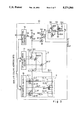
- FIG. 1 of the drawings A typical example of the read only memory device is illustrated in FIG. 1 of the drawings, and comprises a memory cell array 1, a column selector unit 2, a p-channel enhancement type charging transistor 3 and an output inverting circuit 4.
- the memory cell array 1 has a plurality of addressable cell locations CL11, CL1n, CL21, CL2n, CLm1, CLmn, and is associated with a plurality of word lines WL1, WL2 and WLm and with a plurality of digit lines DL1, DL2 and DLn.
- the word lines WL1 to WLm and the digit lines DL1 to DLn define the plurality of addressable memory locations CL11 to CLmn, and n-channel enhancement type memory transistors Qn11, Qn12 and Qn13 are selectively assigned to the cell locations CL11 to CLmn.
- the word lines WL1 to WLm are coupled with a row address decoder 5, and the row address decoder 5 is responsive to row address bits so that one of the word lines WL1 to WLm goes up to active high voltage level. If the selected word line is coupled to a gate electrode of an n-channel enhancement type memory transistor, the n-channel enhancement type memory transistor turns on, and a current path is provided from the associated digit line to a ground voltage line. However, if any n-channel enhancement type memory transistor is not coupled with the selected word line, the digit lines DL1 to DLn are isolated from the ground voltage line.
- the column selector unit 2 is implemented by a plurality of n-channel enhancement type transfer transistors Qn21, Qn22 and Qn2n, and the n-channel enhancement type transfer transistors Qn21 to Qn2n are provided in association with the digit lines DL1 to DLn. Namely, the n-channel enhancement type transfer transistors Qn21 to Qn2n are coupled with the digit lines DL1 to DLn, and are selectively gated by a column address decoder unit 6.
- the column selector unit 2 is further coupled with the p-channel enhancement type charging transistor 3, and the p-channel enhancement type charging transistor 3 is responsive to a control signal CB so as to supply current from a power voltage line Vcc to the column selector unit 2.
- a cell location selected by a word line provides a current path from the selected digit line to the ground voltage line, the current passes through the column selector unit 2 and the current path in the selected cell location, and the voltage level at the drain node N1 of the p-channel enhancement type charging transistor 3 goes down. However, if any current path is established in the selected cell location, the voltage level at the drain node N1 of the p-channel enhancement type charging transistor 3 is maintained in the high voltage level.
- the output inverting circuit 4 is implemented by a series combination of a p-channel enhancement type field effect transistor Qp41 and an n-channel enhancement type field effect transistor Qn42 coupled between the power voltage line Vcc and the ground voltage line, and the drain node N1 of the p-channel enhancement type charging transistor 3 is coupled with the gate electrode of the p-channel enhancement type field effect transistor Qp41 and the gate electrode of the n-channel enhancement type field effect transistor Qn42.
- the common drain node N2 in the series combination is coupled with a data output pin DT, and an output data signal Dout is supplied from the output inverting circuit 4 to the data output pin DT.
- FIG. 2 illustrates a read-out sequence of the prior art read only memory device, and the cell location CL21 is assumed to be accessed twice after access to the cell location CL11.
- the control signal CB is decayed to low voltage level at time t1, and the power voltage line Vcc is coupled with the digit line DL1 through the p-channel enhancement type charging transistor 3 and the n-channel enhancement type transfer transistor Qn21 already selected by the column address decoder unit 6.
- the drain node N1 Since all of the word lines WL1 to WLm are decayed to the low voltage level substantially concurrently with the control signal CB, the drain node N1 is elevated to the power voltage level Vcc, and the digit line DL1 is lifted to an intermediate voltage level V1 lower than the power voltage level Vcc by the threshold level thereof.
- the drain node N1 of the power voltage level Vcc causes the n-channel enhancement type field effect transistor Qn42 to turn on, and the p-channel enhancement type field effect transistor Qp41 turns off.
- the common drain node N2 is coupled through the n-channel enhancement type field effect transistor Qn42 with the ground voltage line, and the output data signal Dout goes down to the ground voltage level at time t2.
- the control signal CB is recovered to the power voltage level Vcc at time t3, and the p-channel enhancement type charging transistor 3 turns off.
- the row address bits causes the row address decoder unit 5 to lift the word line WL1 upon recovery of the control signal CB, and the n-channel enhancement type memory transistor Qn11 turns on to provide the current path from the associated digit line DL1 to the ground voltage line. Current flows from the digit line DL1 to the ground voltage line, and the digit line DL1 is decayed toward the ground voltage level. The digit line DL1 thus decayed allows the n-channel enhancement type transfer transistor Qn21 to turn on, and, accordingly, the drain node N1 goes down toward the ground voltage level.
- the drain node N1 Since the parasitic capacitance coupled with the drain node N1 is much smaller than that coupled with the digit line DL1, the drain node N1 initially goes down at high speed, and, thereafter, is slowly decayed together with the digit line DL1 depending upon the current driving capability of the n-channel enhancement type memory transistor Qn11. Then, the output inverting circuit 4 couples the power voltage line Vcc through the p-channel enhancement type field effect transistor Qp41 with the common drain node N2, and this results in the output data signal Dout of the high voltage level.
- the control signal CB goes down at time t5, and the drain node N1 and the digit line DL1 are precharged as similar to the access to the cell location CL11.
- the word line WL2 goes up at time t6; however, both of the digit line DL1 and the drain node N1 are kept at the respective voltage level V1 and Vcc, because any current path is not provided from the digit line DL1 to the ground voltage line.
- the drain node N1 at the power voltage level Vcc causes the output inverting circuit 4 to couple the common drain node N2 through the n-channel enhancement type field effect transistor Qn42 with the ground voltage line, and the output data signal Dout remains in the low or ground voltage level.
- the control signal CB goes down to the ground voltage level at time t7, and the digit line DL1 and the drain node N1 are precharged again as similar to the previous access.
- the control signal CB is recovered to the high voltage level at time t8, and the word line WL2 goes up upon recovery of the control signal CB.
- noise takes place on the ground voltage line at time t9, the voltage level on the digit line DL1 fluctuates due to the noise, because most of the parasitic capacitance is coupled between the digit line DL1 and the ground voltage line.
- a read only memory device usually internally has various noise sources, and the noise sources are causative of the voltage fluctuation.
- the n-channel enhancement type transfer transistor Qn21 turns on, and the drain node N1 is rapidly decayed, because the parasitic capacitance coupled with the drain node N1 is much smaller than that of the digit line DL1.
- the digit line DL1 is recovered to the high voltage level V1, and the n-channel enhancement type transfer transistor Qn21 turns off. For this reason, the drain node N1 is confined at the voltage level lower than the threshold level of the output inverting circuit 4, and the output data signal Dout goes up to a high voltage level.
- the prior art read only memory device is susceptible to noise on the ground voltage line, and such a low noise margin deteriorates the reliability of the output data signal Dout.
- the present invention proposes to decrease differential voltage level between a precharging level at an input node of an output inverting circuit and a precharging level on a digit line.
- a read only memory device comprising: a) a memory cell array having a plurality of addressable cell locations arranged in rows and columns, enhancement type memory transistors of a first channel conductivity type being assigned to cell locations selected from the plurality of addressable cell locations; b) a plurality of word lines respectively associated with the rows of the addressable cell locations, and coupled with the gate electrodes of the enhancement type memory transistors of the associated rows, respectively, so that one of the rows is selected from the memory cell array; c) a plurality of digit lines respectively associated with the columns of the addressable cell locations, and connectable with a first constant voltage line through the enhancement type memory transistors in the aforesaid one of the rows selected from the memory cell array; d) a column selector unit having a common node, and a plurality of enhancement type transfer transistors of the first channel conductivity type coupled between the plurality of digit lines and the common node, one of the plurality of enhancement type transfer transistors turning on so as to
- FIG. 1 is a circuit diagram showing the circuit arrangement of the prior art read only memory device
- FIG. 2 is a diagram showing the waveforms of voltage levels at essential nodes of the prior art read only memory device
- FIG. 3 is a circuit diagram showing the circuit arrangement of a read only memory device according to the present invention.
- FIG. 4 is a diagram showing the waveforms of essential nodes of the read only memory device shown in FIG. 3;
- FIG. 5 is a circuit diagram showing the circuit arrangement of another read only memory device according to the present invention.
- FIG. 6 is a circuit diagram showing the circuit arrangement of yet another read only memory device according to the present invention.
- FIG. 7 is a circuit diagram showing a floating gate type field effect transistor used for a memory cell instead of an enhancement type field effect transistor incorporated in the embodiments.
- a read only memory device embodying the present invention is fabricated on a single semiconductor chip 10, and comprises a memory cell array 11, a column selector unit 12, an n-channel enhancement type charging transistor 13, an output inverting circuit 14, and a constant voltage producing circuit 15.
- the memory cell array 11 has a plurality of addressable cell locations CL11, CL1n, CL21, CL2n, CLm1, CLmn, and is associated with a plurality of word lines WL1, WL2 and WLm and with a plurality of digit lines DL1, DL2 and DLn.
- the word lines WL1 to WLm and the digit lines DL1 to DLn define the plurality of addressable memory locations CL11 to CLmn, and n-channel enhancement type memory transistors Qn11, Qn12 and Qn13 are selectively assigned to the cell locations CL11 to CLmn.
- the word lines WL1 to WLm are coupled with a row address decoder 16, and the row address decoder 16 is responsive to row address bits so that one of the word lines WL1 to WLm goes up to active high voltage level. If the selected word line is coupled to a gate electrode of an n-channel enhancement type memory transistor, the n-channel enhancement type memory transistor turns on, and a current path is provided from the associated digit line to a ground voltage line. However, if any n-channel enhancement type memory transistor is not coupled with the selected word line, the digit lines DL1 to DLn are isolated from the ground voltage line.
- the column selector unit 12 is implemented by a plurality of n-channel enhancement type transfer transistors Qn21, Qn22 and Qn2n, and the n-channel enhancement type transfer transistors Qn21 to Qn2n are provided in association with the digit lines DL1 to DLn. Namely, the n-channel enhancement type transfer transistors Qn21 to Qn2n are coupled between the associated digit lines DL1 to DLn and a common node N11, and are selectively gated by a column address decoder unit 17.
- the column selector unit 12 is further coupled with the n-channel enhancement type charging transistor 13, and the n-channel enhancement type charging transistor 13 is responsive to a control signal CB supplied from a control signal generator 18 so as to supply current from a power voltage line Vcc to the column selector unit 12.
- a control signal CB supplied from a control signal generator 18 so as to supply current from a power voltage line Vcc to the column selector unit 12.
- a cell location selected by a word line provides a current path from the selected digit line to the ground voltage line
- the current flows from the n-channel enhancement type charging transistor 13 through the column selector unit 12 and the current path in the selected cell location, and the voltage level at the drain node N12 of the n-channel enhancement type charging transistor 13 goes down.
- the voltage level at the drain node N12 of the n-channel enhancement type charging transistor 13 is maintained in the high voltage level.
- the output inverting circuit 14 is implemented by a series combination of a p-channel enhancement type field effect transistor Qp41 and an n-channel enhancement type field effect transistor Qn42 coupled between the power voltage line Vcc and the ground voltage line, and the drain node N12 of the n-channel enhancement type charging transistor 13 is coupled with the gate electrode of the n-channel enhancement type field effect transistor Qn42 only.
- the connection between the drain node N12 and the output inverting circuit 14 is another difference from the prior art read only memory device.
- the gate electrode of the p-channel enhancement type field effect transistor Qp41 is coupled with the output node N14 of the constant voltage generating circuit 15. For this reason, the p-channel enhancement type field effect transistor Qp41 serves as a load element.
- the common drain node N13 in the series combination is coupled with a data output pin DT, and an output data signal Dout is supplied from the output inverting circuit 14 to the data output pin DT.
- the constant voltage generating circuit 15 comprises a series combination of a p-channel enhancement type load transistor Qp51 and an n-channel enhancement type load transistor Qn52 coupled between the power voltage line Vcc and the ground voltage line, and a series combination of an n-channel enhancement type load transistor Qn53 and a resistive element R54 also coupled between the power voltage line Vcc and the ground voltage line.
- the gate electrode of the n-channel enhancement type load transistor Qn53 is coupled with the power voltage line Vcc, and produces a constant step-down voltage level at the drain node thereof.
- the gate electrode of the p-channel enhancement type load transistor Qp51 is coupled with the output node N14 of the constant voltage generating circuit 15, and the drain node of the n-channel enhancement type load transistor Qn53 is coupled with the gate electrode of the n-channel enhancement type load transistor Qn52.
- the n-channel enhancement type load transistor Qn52 provides constant channel resistance against current passing therethrough, and keeps the voltage level at the output node N14 constant in cooperation with the p-channel enhancement type load transistor Qp51.
- FIG. 4 illustrates a read-out sequence of the prior art read only memory device, and the cell locations CL11 and CL21 are assumed to be sequentially accessed in the read-out sequence.
- the control signal CB is lifted to the power voltage level Vcc at time t11, and the n-channel enhancement type charging transistor 13 turns on so that the drain node N12 and, accordingly, the common node N11 are coupled with the power voltage line Vcc. Since the n-channel enhancement type transfer transistor Qn21 has turned on, the power voltage line Vcc is further coupled with the digit line DL1 through the n-channel enhancement type transfer transistor Qn21.
- All of the word lines WL1 to WLm are decayed to the low voltage level at time t12.
- the control signal CB remains in the power voltage level.
- the drain node N12 and, accordingly, the common node N11 go up to a predetermined intermediate voltage level V11 lower than the power voltage level Vcc by the threshold level of the charging transistor 13. Since the n-channel enhancement type transfer transistor Qn21 is approximately equal in threshold level to the n-channel enhancement type charging transistor 13, the digit line DL1 is also lifted to the predetermined intermediate voltage level V11, and is balanced with the drain node N12. Thus, the difference between the drain node N12 and the selected digit line DL1 is minimized in this instance.
- the drain node N12 of the predetermined intermediate voltage level V11 causes the n-channel enhancement type field effect transistor Qn42 to turn on, and the common drain node N13 is coupled through the n-channel enhancement type field effect transistor Qn42 with the ground voltage line. For this reason, the output data signal Dout goes down to the low voltage level at time t13.
- the control signal CB is recovered to the low or ground voltage level at time t14, and the n-channel enhancement type charging transistor 13 turns off.
- the row address bits causes the row address decoder unit 16 to lift the word line wL1 upon recovery of the control signal CB, and the n-channel enhancement type memory transistor Qn11 turns on to provide the current path from the associated digit line DL1 to the ground voltage line. Current flows from the digit line DL1 to the ground voltage line, and the digit line DL1 is decayed toward the ground voltage level. The digit line DL1 thus decayed allows the n-channel enhancement type transfer transistor Qn21 to turn on, and, accordingly, the drain node N12 goes down toward the ground voltage level.
- the output inverting circuit 14 couples the power voltage line Vcc through the p-channel enhancement type field effect transistor Qp41 with the common drain node N13, and this results in the output data signal Dout of the high voltage level at time t15.
- the control signal CB goes up at time t16, and the drain node N12 and the digit line DL1 are precharged to the predetermined intermediate voltage level V11 as similar to the access to the cell location CL11.
- the word line WL2 goes up at time t17; however, both of the digit line DL1 and the drain node N12 are kept at the predetermined intermediate voltage level V11, because any current path is not provided from the digit line DL1 to the ground voltage line.
- the drain node N12 at the predetermined intermediate voltage level V11 causes the output inverting circuit 14 to couple the common drain node N13 through the n-channel enhancement type field effect transistor Qn42 with the ground voltage line, and the output data signal Dout remains in the low voltage level.
- the voltage level on the digit line DL1 fluctuates due to the noise.
- the difference between the drain node N12 and the digit line DL1 has been balanced with one another, and the fluctuation on the digit line DL1 is less causative of fluctuation in voltage level at the drain node N12.
- the drain node N12 does not widely swing the voltage level, and, for this reason, the output inverting circuit 14 keeps the output data signal Dout in the low voltage level.
- the difference in voltage level between the drain node N12 and the selected digit line DL1 is minimized upon completion of the precharging phase, and noise on the digit line DL1 has merely small influence on the voltage level at the drain node N12. For this reason, the output inverting circuit 14 maintains the output data signal Dout, and the reliability is enhanced.
- FIG. 5 of the drawings another read only memory device embodying the present invention is illustrated, and the circuit components thereof are similar to those of the first embodiment except for connections between the drain node N12, the output inverting circuit 14 and the constant voltage generating circuit 15. For this reason, the component elements of the second embodiment are labeled with the same references as the first embodiment.
- the drain node N12 of the n-channel enhancement type charging transistor is coupled with the gate electrode of the p-channel enhancement type load transistor Qp41, and the output node N14 of the constant voltage generating circuit 15 is coupled with the gate electrode of the n-channel enhancement type load transistor Qn42.
- the connections are exchanged, and the connections between the circuit components Qp51 and Qn52 are modified in accordance therewith.
- the output inverting circuit 14 becomes responsive to the voltage level V12 at the drain node N12 when the following equation is satisfied.
- Vth42 is the threshold level of the n-channel enhancement type field effect transistor Qn42
- Vth' is the threshold level of the n-channel enhancement type charging transistor 13 in which the back gate biasing effect is taken into account.
- the second embodiment there is possibility to swing until a larger one between the threshold level Vth42 and the absolute value of the threshold level of the p-channel enhancement type field effect transistor Qp41.
- all of the advantages of the first embodiment are also achieved by the second embodiment.
- FIG. 6 of the drawings yet another read only memory device embodying the present invention is illustrated.
- the read only memory device implementing the third embodiment is similar to the first embodiment except for the memory cell array 11 associated with a block decoder 51 as well as n-channel enhancement type selecting transistors Qn61 to Qn6x, and, for this reason, circuit components are labeled with the same references as those designating the corresponding circuit components of the first embodiment.
- the memory cell array 11 is broken down into a plurality of memory cell sub-arrays 111 to 11x, and the word lines WL1 to WL4 and digit lines DL1 to DLn are shared between the memory cell sub-arrays 111 to 11x.
- the block decoder 51 is coupled through decoded signal lines BL1 to BLx with the n-channel enhancement type selecting transistors Qn61 to Qn6x, and selects one of the memory cell sub-arrays 111 to 11x from the memory cell array 11.
- the other circuit components behave on the selected memory cell sub-array as similar to those of the first embodiment, and no further description is incorporated hereinbelow.
- a boosted power voltage level may be supplied to some circuit components for enhancing the stability of circuit behavior.
- the read only memory device may be incorporated in an ultra large scale integration such as, for example, a microprocessor or a semi-custom made integrated circuit device.
- the memory cell arrays 11 of the first to third embodiments are implemented by n-channel enhancement type memory transistors.
- a memory cell array incorporated in a read only memory device according to the present invention may be implemented by a plurality of floating gate type field effect transistors FG each having the structure shown in FIG. 7.
- the floating gate type field effect transistors FG allows the read only memory device to serve as an electrically programmable read only memory device or as an electrically erasable and programmable read only memory device.
Landscapes
- Read Only Memory (AREA)
Applications Claiming Priority (2)
| Application Number | Priority Date | Filing Date | Title |
|---|---|---|---|
| JP18309691A JP3313383B2 (ja) | 1991-06-27 | 1991-06-27 | 読み出し専用記憶装置 |
| JP3-183096 | 1991-06-27 |
Publications (1)
| Publication Number | Publication Date |
|---|---|
| US5274590A true US5274590A (en) | 1993-12-28 |
Family
ID=16129697
Family Applications (1)
| Application Number | Title | Priority Date | Filing Date |
|---|---|---|---|
| US07/901,688 Expired - Fee Related US5274590A (en) | 1991-06-27 | 1992-06-22 | Read only memory device with recharging transistor automatically supplementing current to an input node of output invertor |
Country Status (5)
| Country | Link |
|---|---|
| US (1) | US5274590A (fr) |
| EP (1) | EP0520357B1 (fr) |
| JP (1) | JP3313383B2 (fr) |
| KR (1) | KR950002728B1 (fr) |
| DE (1) | DE69220144T2 (fr) |
Cited By (4)
| Publication number | Priority date | Publication date | Assignee | Title |
|---|---|---|---|---|
| US5357474A (en) * | 1992-10-19 | 1994-10-18 | Nec Corporation | Dynamic random access memory device having precharge circuit for intermittently and selectively charging data line pairs |
| US5539700A (en) * | 1992-11-10 | 1996-07-23 | Matsushita Electric Industrial Co., Ltd. | Column selection circuit of semiconductor memory with transfer gate |
| US5691944A (en) * | 1995-04-21 | 1997-11-25 | Nec Corporation | Non-volatile semiconductor memory device |
| US5706237A (en) * | 1996-10-08 | 1998-01-06 | International Business Machines Corporation | Self-restore circuit with soft error protection for dynamic logic circuits |
Families Citing this family (1)
| Publication number | Priority date | Publication date | Assignee | Title |
|---|---|---|---|---|
| JPH0745086A (ja) * | 1993-08-02 | 1995-02-14 | Mitsubishi Electric Corp | メモリ装置 |
Citations (3)
| Publication number | Priority date | Publication date | Assignee | Title |
|---|---|---|---|---|
| US4843594A (en) * | 1985-08-01 | 1989-06-27 | Kabushiki Kaisha Toshiba | Nonvolatile semiconductor memory device with a bias circuit |
| JPH01251499A (ja) * | 1988-03-31 | 1989-10-06 | Toshiba Corp | 不揮発性半導体記憶装置 |
| US5001668A (en) * | 1988-03-09 | 1991-03-19 | Kabushiki Kaisha Toshiba | Nonvolatile memory circuit device with low power consumption and wide operating voltage range |
Family Cites Families (3)
| Publication number | Priority date | Publication date | Assignee | Title |
|---|---|---|---|---|
| JPH0766675B2 (ja) * | 1987-07-14 | 1995-07-19 | 株式会社東芝 | プログラマブルrom |
| JP2513795B2 (ja) * | 1988-07-22 | 1996-07-03 | 沖電気工業株式会社 | Mos型半導体記憶装置 |
| JPH0724298B2 (ja) * | 1988-08-10 | 1995-03-15 | 日本電気株式会社 | 半導体記憶装置 |
-
1991
- 1991-06-27 JP JP18309691A patent/JP3313383B2/ja not_active Expired - Fee Related
-
1992
- 1992-06-22 US US07/901,688 patent/US5274590A/en not_active Expired - Fee Related
- 1992-06-22 EP EP92110515A patent/EP0520357B1/fr not_active Expired - Lifetime
- 1992-06-22 DE DE69220144T patent/DE69220144T2/de not_active Expired - Fee Related
- 1992-06-25 KR KR1019920011077A patent/KR950002728B1/ko not_active Expired - Fee Related
Patent Citations (3)
| Publication number | Priority date | Publication date | Assignee | Title |
|---|---|---|---|---|
| US4843594A (en) * | 1985-08-01 | 1989-06-27 | Kabushiki Kaisha Toshiba | Nonvolatile semiconductor memory device with a bias circuit |
| US5001668A (en) * | 1988-03-09 | 1991-03-19 | Kabushiki Kaisha Toshiba | Nonvolatile memory circuit device with low power consumption and wide operating voltage range |
| JPH01251499A (ja) * | 1988-03-31 | 1989-10-06 | Toshiba Corp | 不揮発性半導体記憶装置 |
Cited By (4)
| Publication number | Priority date | Publication date | Assignee | Title |
|---|---|---|---|---|
| US5357474A (en) * | 1992-10-19 | 1994-10-18 | Nec Corporation | Dynamic random access memory device having precharge circuit for intermittently and selectively charging data line pairs |
| US5539700A (en) * | 1992-11-10 | 1996-07-23 | Matsushita Electric Industrial Co., Ltd. | Column selection circuit of semiconductor memory with transfer gate |
| US5691944A (en) * | 1995-04-21 | 1997-11-25 | Nec Corporation | Non-volatile semiconductor memory device |
| US5706237A (en) * | 1996-10-08 | 1998-01-06 | International Business Machines Corporation | Self-restore circuit with soft error protection for dynamic logic circuits |
Also Published As
| Publication number | Publication date |
|---|---|
| KR950002728B1 (ko) | 1995-03-24 |
| JP3313383B2 (ja) | 2002-08-12 |
| EP0520357A3 (en) | 1995-04-05 |
| EP0520357A2 (fr) | 1992-12-30 |
| DE69220144T2 (de) | 1998-01-22 |
| DE69220144D1 (de) | 1997-07-10 |
| JPH056686A (ja) | 1993-01-14 |
| EP0520357B1 (fr) | 1997-06-04 |
Similar Documents
| Publication | Publication Date | Title |
|---|---|---|
| JP2507529B2 (ja) | 不揮発性半導体記憶装置 | |
| US4094012A (en) | Electrically programmable MOS read-only memory with isolated decoders | |
| US5040146A (en) | Static memory cell | |
| US7099188B1 (en) | Bit line reference circuits for binary and multiple-bit-per-cell memories | |
| US5243573A (en) | Sense amplifier for nonvolatile semiconductor storage devices | |
| US5255233A (en) | Non-volatile semiconductor memory device equipped with sense amplifier circuit for discriminating small differential voltage level | |
| US6456548B2 (en) | Sense amplifier circuit and semiconductor storage device | |
| US4709165A (en) | Voltage supply level detecting circuit | |
| EP0199501A2 (fr) | Amplificateurs CMOS détecteurs de courant | |
| US5477484A (en) | Semiconductor memory having a high speed sense amplifier | |
| US5790466A (en) | Multiple precharging semiconductor memory device | |
| US5029138A (en) | Sense amplifier circuit coupled to a bit line pair for increasing a difference in voltage level at an improved speed | |
| US4962482A (en) | Nonvolatile memory device using a sense circuit including variable threshold transistors | |
| US5371703A (en) | Single-bit output type memory including bipolar selection transistors | |
| US4794571A (en) | Dynamic read-write random access memory | |
| EP0332135B1 (fr) | Circuit de mémoire non volatile ayant une faible consommation de courant et une plage de tension de fonctionnement étendue | |
| US5528544A (en) | Semiconductor memory device having high speed sense amplifier | |
| US6600672B2 (en) | Semiconductor memory device | |
| US6141277A (en) | Semiconductor memory preventing sense amplifier malfunctions due to effects of noise generated in output buffer | |
| US5933373A (en) | Semiconductor memory device having constant potential generator for clamping digit lines at constant level allowing precharge transistor to slightly turn on | |
| US7082058B2 (en) | Non-volatile semiconductor memory device having sense amplifier with increased speed | |
| US4939691A (en) | Static random access memory | |
| US5018108A (en) | Nonvolatile semiconductor memory | |
| US7099214B2 (en) | Semiconductor memory device | |
| US5274590A (en) | Read only memory device with recharging transistor automatically supplementing current to an input node of output invertor |
Legal Events
| Date | Code | Title | Description |
|---|---|---|---|
| AS | Assignment |
Owner name: NEC CORPORATION, JAPAN Free format text: ASSIGNMENT OF ASSIGNORS INTEREST.;ASSIGNOR:KASHIMURA, MASAHIKO;REEL/FRAME:006165/0145 Effective date: 19920605 |
|
| FEPP | Fee payment procedure |
Free format text: PAYOR NUMBER ASSIGNED (ORIGINAL EVENT CODE: ASPN); ENTITY STATUS OF PATENT OWNER: LARGE ENTITY |
|
| FPAY | Fee payment |
Year of fee payment: 4 |
|
| FEPP | Fee payment procedure |
Free format text: PAYER NUMBER DE-ASSIGNED (ORIGINAL EVENT CODE: RMPN); ENTITY STATUS OF PATENT OWNER: LARGE ENTITY Free format text: PAYOR NUMBER ASSIGNED (ORIGINAL EVENT CODE: ASPN); ENTITY STATUS OF PATENT OWNER: LARGE ENTITY |
|
| FPAY | Fee payment |
Year of fee payment: 8 |
|
| REMI | Maintenance fee reminder mailed | ||
| LAPS | Lapse for failure to pay maintenance fees | ||
| STCH | Information on status: patent discontinuation |
Free format text: PATENT EXPIRED DUE TO NONPAYMENT OF MAINTENANCE FEES UNDER 37 CFR 1.362 |
|
| FP | Lapsed due to failure to pay maintenance fee |
Effective date: 20051228 |