US5299727A - Method of manufacture of an optoelectronic coupling element - Google Patents
Method of manufacture of an optoelectronic coupling element Download PDFInfo
- Publication number
- US5299727A US5299727A US08/045,665 US4566593A US5299727A US 5299727 A US5299727 A US 5299727A US 4566593 A US4566593 A US 4566593A US 5299727 A US5299727 A US 5299727A
- Authority
- US
- United States
- Prior art keywords
- plug
- optoelectronic
- receptacle
- housing
- contact strips
- Prior art date
- Legal status (The legal status is an assumption and is not a legal conclusion. Google has not performed a legal analysis and makes no representation as to the accuracy of the status listed.)
- Expired - Lifetime
Links
Images

Classifications
-
- H—ELECTRICITY
- H10—SEMICONDUCTOR DEVICES; ELECTRIC SOLID-STATE DEVICES NOT OTHERWISE PROVIDED FOR
- H10F—INORGANIC SEMICONDUCTOR DEVICES SENSITIVE TO INFRARED RADIATION, LIGHT, ELECTROMAGNETIC RADIATION OF SHORTER WAVELENGTH OR CORPUSCULAR RADIATION
- H10F55/00—Radiation-sensitive semiconductor devices covered by groups H10F10/00, H10F19/00 or H10F30/00 being structurally associated with electric light sources and electrically or optically coupled thereto
- H10F55/20—Radiation-sensitive semiconductor devices covered by groups H10F10/00, H10F19/00 or H10F30/00 being structurally associated with electric light sources and electrically or optically coupled thereto wherein the electric light source controls the radiation-sensitive semiconductor devices, e.g. optocouplers
- H10F55/25—Radiation-sensitive semiconductor devices covered by groups H10F10/00, H10F19/00 or H10F30/00 being structurally associated with electric light sources and electrically or optically coupled thereto wherein the electric light source controls the radiation-sensitive semiconductor devices, e.g. optocouplers wherein the radiation-sensitive devices and the electric light source are all semiconductor devices
-
- H—ELECTRICITY
- H10—SEMICONDUCTOR DEVICES; ELECTRIC SOLID-STATE DEVICES NOT OTHERWISE PROVIDED FOR
- H10W—GENERIC PACKAGES, INTERCONNECTIONS, CONNECTORS OR OTHER CONSTRUCTIONAL DETAILS OF DEVICES COVERED BY CLASS H10
- H10W72/00—Interconnections or connectors in packages
- H10W72/50—Bond wires
- H10W72/531—Shapes of wire connectors
- H10W72/536—Shapes of wire connectors the connected ends being ball-shaped
-
- H—ELECTRICITY
- H10—SEMICONDUCTOR DEVICES; ELECTRIC SOLID-STATE DEVICES NOT OTHERWISE PROVIDED FOR
- H10W—GENERIC PACKAGES, INTERCONNECTIONS, CONNECTORS OR OTHER CONSTRUCTIONAL DETAILS OF DEVICES COVERED BY CLASS H10
- H10W72/00—Interconnections or connectors in packages
- H10W72/50—Bond wires
- H10W72/531—Shapes of wire connectors
- H10W72/5363—Shapes of wire connectors the connected ends being wedge-shaped
-
- H—ELECTRICITY
- H10—SEMICONDUCTOR DEVICES; ELECTRIC SOLID-STATE DEVICES NOT OTHERWISE PROVIDED FOR
- H10W—GENERIC PACKAGES, INTERCONNECTIONS, CONNECTORS OR OTHER CONSTRUCTIONAL DETAILS OF DEVICES COVERED BY CLASS H10
- H10W90/00—Package configurations
- H10W90/701—Package configurations characterised by the relative positions of pads or connectors relative to package parts
- H10W90/751—Package configurations characterised by the relative positions of pads or connectors relative to package parts of bond wires
- H10W90/756—Package configurations characterised by the relative positions of pads or connectors relative to package parts of bond wires between a chip and a stacked lead frame, conducting package substrate or heat sink
-
- Y—GENERAL TAGGING OF NEW TECHNOLOGICAL DEVELOPMENTS; GENERAL TAGGING OF CROSS-SECTIONAL TECHNOLOGIES SPANNING OVER SEVERAL SECTIONS OF THE IPC; TECHNICAL SUBJECTS COVERED BY FORMER USPC CROSS-REFERENCE ART COLLECTIONS [XRACs] AND DIGESTS
- Y10—TECHNICAL SUBJECTS COVERED BY FORMER USPC
- Y10T—TECHNICAL SUBJECTS COVERED BY FORMER US CLASSIFICATION
- Y10T29/00—Metal working
- Y10T29/49—Method of mechanical manufacture
- Y10T29/49002—Electrical device making
- Y10T29/49117—Conductor or circuit manufacturing
- Y10T29/49194—Assembling elongated conductors, e.g., splicing, etc.
Definitions
- the invention relates to a method for manufacture of an optoelectronic coupling element.
- the optoelectronic elements are accommodated in complete housings and are surrounded on all sides by the housing material, these housings are best comprised of transparent, light-permeable material. This results in a not inconsiderable emission of the luminous power from the transmitter to the outside. Added to the problem of insufficient coupling is that of extraneous light incidence from the outside, which further reduces the quality of an optocoupler of this type.
- a second outer housing is provided that completely surrounds the first housing.
- these measures necessitate a number of additional production steps.
- the object underlying the invention is to provide a method for manufacture of an optoelectronic coupling element where the housing comprises two sections that can be fitted together and which each hold at least one optoelectronic semiconductor element, with one section being designed as a plug and the other as a receptacle, avoiding the aforementioned drawbacks.
- the two contact strips are embedded in a plastic in a first process step.
- One strip is designed as a plug and a second strip as a receptacle.
- the plug and the receptacle have cutouts to hold the optoelectronic elements.
- the contact strips are exposed such that the optoelectronic semiconductor elements can be electrically connected.
- the housing sections are joined together in a concluding process step. The connection of the housing sections is then fixed. This can be achieved with the aid of a grid in the plug connection, while another embodiment of the method provides for glueing or welding of the housing.
- the optoelectronic semiconductor elements are each provided with a drop of resin before the housing sections are joined together.
- the resin drops of the opposite elements mingle and thus provide the optical connection.
- the housing sections are fixed.
- the housing sections are manufactured in a block-shaped basic form. This permits the finished elements to be processed by automatic PCB component insertion facilities.
- One particular advantage of the method in accordance with the invention is that the optoelectronic semiconductor elements are not embedded in the plastic of the housing sections, but are mounted on prefabricated housing sections. It is therefore possible to select any transparent, opaque or light-impermeable plastics for the housing material. In the normal case, a light-impermeable plastic will be selected, so that the housing is optically tight.
- the resin drop between the semiconductor elements increases on the one hand the optical coupling factor and on the other hand the electrical high-voltage resistance of the element produced in accordance with the invention.
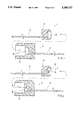
- FIG. 1 shows contact strips surrounded by plastic in one stage of the method
- FIG. 2 shows contact strips with attached element in a further stage of the method
- FIG. 3 shows a section through the optoelectronic coupling element in a side view
- FIG. 4 shows a section through the optoelectronic coupling element in a plan view.
- FIG. 1 shows the two housing sections 1, 2 of the optoelectronic coupling element in a first stage of the manufacturing process in accordance with the invention.
- the contact strips 3 comprise a row of connection lugs having a common carrier strip.
- the connection lugs are divided up into groups that are surrounded with plastic 4 to form a housing section 1, 2.
- Plug 1 and receptacle 2 therefore each have 4 connection lugs in this embodiment, so that a total of 8 lugs are available in the finished optoelectronic coupling element.
- the number of connection lugs is only predetermined by the number of electrical feed lines required by the elements 5, 6, and is otherwise freely selectable. This means that it is quite possible to fit several elements in each housing section.
- These groups of connection lugs hereafter referred to in brief as contact strips 3, are surrounded by a plastic molded piece 4 in a first process step using known techniques, for example injection molding.
- These plastic molded pieces 4 are designed as a plug 1 for one part and as a receptacle 2 for the other part of the contact strip.
- the plastic molded piece 4 of the plug 1 can be inserted into the matching receptacle 2 for a positive connection.
- the exact shapes of plug 1 and receptacle 2 depend on the required housing shape of the optoelectronic coupler and can be adjusted to that shape by design measures.
- the insides of the plug and the receptacle each have a cutout 8. Parts of the contact strips 3 are exposedin these cutouts 8. In the embodiment, the ends of the contact strip 3 thatare enclosed by the plastic molded piece are angled. The angled longitudinal side of the contact strip 3 is exposed on the bottom of the cutout 8. In the assembled state, the bottoms of the cutouts 8 of plug 1 and receptacle 2 are opposite to one another.
- FIG. 2 shows the two housing sections 1, 2 of the optoelectronic coupling element in a second stage of the manufacturing method in accordance with the invention.
- the optoelectronic elements 5, 6 are fitted in the cutouts 8 of plug 1 and receptacle 2. Assembly is performed in this embodiment with the aid of the conductive adhesive such that the rear contact of the element 5, 6 is electrically connected to a connecting lug of the contact strip 3.
- the element 5, 6 is soldered to the angled end of the connecting lug, with an electrical contact to the rear electrode of the element 5, 6 being made at the same time.
- Other assembly techniques for example glueing to the plastic moldedpiece 4 in the cutout 8, can also be applied.
- the remaining electrical connections are made from the exposed surface of the optoelectronic element by connecting lines to the connecting lugs provided for that purpose on the contact strip 3. This can be achieved using known wire bondprocesses, for example.
- thecutouts 8 of plug 1 and receptacle 2 are filled with a resin droplet in this embodiment.
- the two resin drops mingle and thereby ensure an improved optical coupling of the elements.
- FIGS. 3 and 4 show sections through an optoelectronic coupling element madeusing the method in accordance with the invention, in a side view and a plan view.
- the two optoelectronic elements 5, 6 are disposed in the cutouts 8 of plug 1 and receptacle 2 such that the elements 5, 6 are substantially opposite to one another.
- the connection of plug 1 and receptacle 2 is fixed by welding of the two housing sections 1, 2 in this embodiment.
- a further embodiment of the method achieves fixing of the connection of plug and receptacle by glueing together the two housing sections.
- additional fixing is achieved by designmeasures in plug 1 and receptacle 2.
- An engaging mechanism secures the connection of the two housing sections 1, 2, either by itself or additionally to the measures already described above.
- the inner area formed by the cutouts 8 is provided with a reflection layer in a further embodiment of the method in accordance with the invention, which reflects the optical radiation.
- the plastic material 4 of the housing sections 1, 2 is selected such that a reflecting surface is obtained in the inner area formed by the cutouts 8.
- the particular advantage of the method in accordance with the invention is that--unlike with known methods for manufacture of optoelectronic couplingelements--the optoelectronic elements are fitted in prefabricated housing sections and the housing sections are then only joined together.
- a moldingprocess can be dispensed with here, since the plastic housing sections can be made using known injection molding techniques, for example.
- the method in accordance with the invention is therefore less expensive and simpler than known methods for the manufacture of optoelectronic coupling elements.
Landscapes
- Optical Couplings Of Light Guides (AREA)
- Led Device Packages (AREA)
- Luminescent Compositions (AREA)
Applications Claiming Priority (2)
| Application Number | Priority Date | Filing Date | Title |
|---|---|---|---|
| DE4214792A DE4214792A1 (de) | 1992-05-04 | 1992-05-04 | Verfahren zum Herstellen eines optoelektronischen Koppelelements |
| DE4214792 | 1992-05-04 |
Publications (1)
| Publication Number | Publication Date |
|---|---|
| US5299727A true US5299727A (en) | 1994-04-05 |
Family
ID=6458185
Family Applications (1)
| Application Number | Title | Priority Date | Filing Date |
|---|---|---|---|
| US08/045,665 Expired - Lifetime US5299727A (en) | 1992-05-04 | 1993-04-09 | Method of manufacture of an optoelectronic coupling element |
Country Status (4)
| Country | Link |
|---|---|
| US (1) | US5299727A (de) |
| EP (1) | EP0568838B1 (de) |
| AT (1) | ATE173562T1 (de) |
| DE (2) | DE4214792A1 (de) |
Cited By (6)
| Publication number | Priority date | Publication date | Assignee | Title |
|---|---|---|---|---|
| EP0704911A3 (de) * | 1994-09-27 | 1998-01-21 | ITT Corporation | Optoelektrischer Koppler |
| WO1999019755A1 (en) * | 1997-10-10 | 1999-04-22 | Corning Incorporated | Optical device having optical component isolated from housing |
| US20070045800A1 (en) * | 2005-08-19 | 2007-03-01 | Brian King | Opto-coupler with high reverse breakdown voltage and high isolation potential |
| US20090140266A1 (en) * | 2007-11-30 | 2009-06-04 | Yong Liu | Package including oriented devices |
| US20100193803A1 (en) * | 2009-02-04 | 2010-08-05 | Yong Liu | Stacked Micro Optocouplers and Methods of Making the Same |
| CN116936480A (zh) * | 2022-06-16 | 2023-10-24 | 成都市汉桐集成技术有限公司 | 芯片的封装结构和封装方法 |
Families Citing this family (3)
| Publication number | Priority date | Publication date | Assignee | Title |
|---|---|---|---|---|
| DE4340864C2 (de) * | 1993-12-01 | 1996-08-01 | Telefunken Microelectron | Vorrichtung und Verfahren zum Herstellen von optoelektronischen Bauelementen |
| FR2792249B1 (fr) | 1999-04-19 | 2001-06-22 | Fort James France | Dispositif d'etancheite d'extremite pour chambre a racle |
| DE102006062599B4 (de) * | 2006-12-29 | 2018-03-08 | Endress + Hauser Gmbh + Co. Kg | Opto-elektronische Vorrichtung zur Übertragung eines elektrischen Signals und deren Verwendung |
Citations (11)
| Publication number | Priority date | Publication date | Assignee | Title |
|---|---|---|---|---|
| DE226431C (de) * | ||||
| DE1614880A1 (de) * | 1967-10-27 | 1970-12-23 | Telefunken Patent | Optoelektronische Koppelanordnung |
| US3878397A (en) * | 1973-06-29 | 1975-04-15 | Itt | Electro-optical transmission line |
| JPS577170A (en) * | 1980-06-16 | 1982-01-14 | Nissin Electric Co Ltd | Photo-coupler |
| DE3211792A1 (de) * | 1982-03-30 | 1983-11-10 | Siemens AG, 1000 Berlin und 8000 München | Lichtwellenleiter-steckverbindung |
| EP0127401A1 (de) * | 1983-05-31 | 1984-12-05 | Sumitomo Electric Industries Limited | Gehäuse für elektrooptisches Bauelement |
| WO1986001458A1 (en) * | 1984-08-31 | 1986-03-13 | Motorola, Inc. | Process for bonding the surfaces of two materials and an improved optocoupler manufactured therewith |
| DE3630382A1 (de) * | 1986-09-05 | 1988-03-10 | Siemens Ag | Loesbare oder feste optische verbindung von zwei optoelektronischen halbleiterbauelementen |
| US4863232A (en) * | 1988-06-16 | 1989-09-05 | Northern Telecom Limited | Optical connector |
| EP0347704A1 (de) * | 1988-06-23 | 1989-12-27 | Heimann Optoelectronics GmbH | Infrarotdetektor |
| US4890894A (en) * | 1988-06-16 | 1990-01-02 | Northern Telecom Limited | Optical connector |
Family Cites Families (1)
| Publication number | Priority date | Publication date | Assignee | Title |
|---|---|---|---|---|
| DD226431A1 (de) * | 1984-08-02 | 1985-08-21 | Werk Fernsehelektronik Veb | Optoelektronisches halbleiterbauelement |
-
1992
- 1992-05-04 DE DE4214792A patent/DE4214792A1/de not_active Withdrawn
-
1993
- 1993-04-09 US US08/045,665 patent/US5299727A/en not_active Expired - Lifetime
- 1993-04-10 DE DE59309131T patent/DE59309131D1/de not_active Expired - Lifetime
- 1993-04-10 AT AT93105900T patent/ATE173562T1/de not_active IP Right Cessation
- 1993-04-10 EP EP93105900A patent/EP0568838B1/de not_active Expired - Lifetime
Patent Citations (11)
| Publication number | Priority date | Publication date | Assignee | Title |
|---|---|---|---|---|
| DE226431C (de) * | ||||
| DE1614880A1 (de) * | 1967-10-27 | 1970-12-23 | Telefunken Patent | Optoelektronische Koppelanordnung |
| US3878397A (en) * | 1973-06-29 | 1975-04-15 | Itt | Electro-optical transmission line |
| JPS577170A (en) * | 1980-06-16 | 1982-01-14 | Nissin Electric Co Ltd | Photo-coupler |
| DE3211792A1 (de) * | 1982-03-30 | 1983-11-10 | Siemens AG, 1000 Berlin und 8000 München | Lichtwellenleiter-steckverbindung |
| EP0127401A1 (de) * | 1983-05-31 | 1984-12-05 | Sumitomo Electric Industries Limited | Gehäuse für elektrooptisches Bauelement |
| WO1986001458A1 (en) * | 1984-08-31 | 1986-03-13 | Motorola, Inc. | Process for bonding the surfaces of two materials and an improved optocoupler manufactured therewith |
| DE3630382A1 (de) * | 1986-09-05 | 1988-03-10 | Siemens Ag | Loesbare oder feste optische verbindung von zwei optoelektronischen halbleiterbauelementen |
| US4863232A (en) * | 1988-06-16 | 1989-09-05 | Northern Telecom Limited | Optical connector |
| US4890894A (en) * | 1988-06-16 | 1990-01-02 | Northern Telecom Limited | Optical connector |
| EP0347704A1 (de) * | 1988-06-23 | 1989-12-27 | Heimann Optoelectronics GmbH | Infrarotdetektor |
Non-Patent Citations (3)
| Title |
|---|
| Motorola Inc., Technical Developments, vol. 14, Dec. 1991, V. J. Adams Pre Assembled Opto . . . . * |
| Patent Abstracts of Japan; vol. 6, No. 67 (E 104)(945), Apr. 28th, 1982 & JP A 57 007 170 (Nitsushin), Jan. 14th, 1982. * |
| Patent Abstracts of Japan; vol. 6, No. 67 (E-104)(945), Apr. 28th, 1982 & JP-A-57 007 170 (Nitsushin), Jan. 14th, 1982. |
Cited By (9)
| Publication number | Priority date | Publication date | Assignee | Title |
|---|---|---|---|---|
| EP0704911A3 (de) * | 1994-09-27 | 1998-01-21 | ITT Corporation | Optoelektrischer Koppler |
| US6091073A (en) * | 1994-09-27 | 2000-07-18 | Itt Corporation | Optoelectric coupler |
| WO1999019755A1 (en) * | 1997-10-10 | 1999-04-22 | Corning Incorporated | Optical device having optical component isolated from housing |
| US6430350B1 (en) | 1997-10-10 | 2002-08-06 | Corning Incorporated | Optical device having an optical component isolated from housing |
| US20070045800A1 (en) * | 2005-08-19 | 2007-03-01 | Brian King | Opto-coupler with high reverse breakdown voltage and high isolation potential |
| US20090140266A1 (en) * | 2007-11-30 | 2009-06-04 | Yong Liu | Package including oriented devices |
| US20100193803A1 (en) * | 2009-02-04 | 2010-08-05 | Yong Liu | Stacked Micro Optocouplers and Methods of Making the Same |
| US7973393B2 (en) | 2009-02-04 | 2011-07-05 | Fairchild Semiconductor Corporation | Stacked micro optocouplers and methods of making the same |
| CN116936480A (zh) * | 2022-06-16 | 2023-10-24 | 成都市汉桐集成技术有限公司 | 芯片的封装结构和封装方法 |
Also Published As
| Publication number | Publication date |
|---|---|
| DE4214792A1 (de) | 1993-11-11 |
| DE59309131D1 (de) | 1998-12-24 |
| EP0568838B1 (de) | 1998-11-18 |
| ATE173562T1 (de) | 1998-12-15 |
| EP0568838A1 (de) | 1993-11-10 |
Similar Documents
| Publication | Publication Date | Title |
|---|---|---|
| US4446375A (en) | Optocoupler having folded lead frame construction | |
| KR0137189B1 (ko) | 광학소자의 개선한 접지를 가진 광모듈 | |
| US5059373A (en) | Method of manufacturing continuous strip of electronic devices | |
| US6988819B2 (en) | Lamp housing containing an integrated LED support structure | |
| JP3176496B2 (ja) | 光結合装置およびその製造方法 | |
| JPH07151932A (ja) | 光電子インターフェース・モジュールとその作成方法 | |
| US5647034A (en) | Operation displaying semiconductor switch | |
| JP5219828B2 (ja) | 光学部品を有する複合装置及び複合装置の製造方法 | |
| US20030136968A1 (en) | Semiconductor package having light sensitive chips | |
| US20010022390A1 (en) | Diode housing | |
| JP2003520991A (ja) | 内部光学導波管を有する光学送受信モジュール | |
| US20050056851A1 (en) | Optoelectronic component and optoelectronic arrangement with an optoelectronic component | |
| JPH06308344A (ja) | 光ファイバを電子回路に結合するためのインターフェース | |
| JPH0756061A (ja) | 反射面を有する光電子インターフェース装置およびその製造法 | |
| JP3383222B2 (ja) | ケーブル接続用コネクタ | |
| US4953006A (en) | Packaging method and package for edge-coupled optoelectronic device | |
| CN102444874A (zh) | Led灯条模块的连接器与散热器的组装与其形成方法 | |
| GB2046472A (en) | Electro-optical connector | |
| JP2966591B2 (ja) | 光半導体装置 | |
| AU607005B2 (en) | An opto-electronic device | |
| EP0568838B1 (de) | Verfahren zum Herstellen eines optoelektronischen Koppelelements | |
| US20050093129A1 (en) | Semiconductor device and manufacturing method thereof | |
| CN105874620B (zh) | 用作完整led封装的深模制反射器杯体 | |
| JP2001127312A5 (de) | ||
| KR940007445Y1 (ko) | 조립식 포토커플라 |
Legal Events
| Date | Code | Title | Description |
|---|---|---|---|
| STPP | Information on status: patent application and granting procedure in general |
Free format text: APPLICATION UNDERGOING PREEXAM PROCESSING |
|
| AS | Assignment |
Owner name: TEMIC TELEFUNKEN MICROELECTRONIC GMBH, GERMANY Free format text: ASSIGNMENT OF ASSIGNORS INTEREST;ASSIGNOR:KOFLER, ALBIN;REEL/FRAME:006792/0084 Effective date: 19930317 |
|
| FEPP | Fee payment procedure |
Free format text: PAYOR NUMBER ASSIGNED (ORIGINAL EVENT CODE: ASPN); ENTITY STATUS OF PATENT OWNER: LARGE ENTITY |
|
| FPAY | Fee payment |
Year of fee payment: 4 |
|
| AS | Assignment |
Owner name: ATMEL CORPORATION, CALIFORNIA Free format text: ASSIGNMENT OF ASSIGNORS INTEREST;ASSIGNOR:ATMEL CORPORATION;REEL/FRAME:010231/0283 Effective date: 19990913 |
|
| FEPP | Fee payment procedure |
Free format text: PAYOR NUMBER ASSIGNED (ORIGINAL EVENT CODE: ASPN); ENTITY STATUS OF PATENT OWNER: LARGE ENTITY Free format text: PAYER NUMBER DE-ASSIGNED (ORIGINAL EVENT CODE: RMPN); ENTITY STATUS OF PATENT OWNER: LARGE ENTITY |
|
| REFU | Refund |
Free format text: REFUND - PAYMENT OF MAINTENANCE FEE, 8TH YEAR, LARGE ENTITY (ORIGINAL EVENT CODE: R184); ENTITY STATUS OF PATENT OWNER: LARGE ENTITY |
|
| FPAY | Fee payment |
Year of fee payment: 8 |
|
| FPAY | Fee payment |
Year of fee payment: 12 |