US5323020A - High performance MESFET with multiple quantum wells - Google Patents
High performance MESFET with multiple quantum wells Download PDFInfo
- Publication number
- US5323020A US5323020A US07/995,459 US99545992A US5323020A US 5323020 A US5323020 A US 5323020A US 99545992 A US99545992 A US 99545992A US 5323020 A US5323020 A US 5323020A
- Authority
- US
- United States
- Prior art keywords
- region
- fet
- channel
- gate
- source
- Prior art date
- Legal status (The legal status is an assumption and is not a legal conclusion. Google has not performed a legal analysis and makes no representation as to the accuracy of the status listed.)
- Expired - Lifetime
Links
Images


Classifications
-
- H—ELECTRICITY
- H10—SEMICONDUCTOR DEVICES; ELECTRIC SOLID-STATE DEVICES NOT OTHERWISE PROVIDED FOR
- H10D—INORGANIC ELECTRIC SEMICONDUCTOR DEVICES
- H10D30/00—Field-effect transistors [FET]
- H10D30/80—FETs having rectifying junction gate electrodes
- H10D30/83—FETs having PN junction gate electrodes
- H10D30/832—Thin-film junction FETs [JFET]
-
- H—ELECTRICITY
- H10—SEMICONDUCTOR DEVICES; ELECTRIC SOLID-STATE DEVICES NOT OTHERWISE PROVIDED FOR
- H10D—INORGANIC ELECTRIC SEMICONDUCTOR DEVICES
- H10D30/00—Field-effect transistors [FET]
- H10D30/40—FETs having zero-dimensional [0D], one-dimensional [1D] or two-dimensional [2D] charge carrier gas channels
- H10D30/47—FETs having zero-dimensional [0D], one-dimensional [1D] or two-dimensional [2D] charge carrier gas channels having two-dimensional [2D] charge carrier gas channels, e.g. nanoribbon FETs or high electron mobility transistors [HEMT]
- H10D30/471—High electron mobility transistors [HEMT] or high hole mobility transistors [HHMT]
- H10D30/473—High electron mobility transistors [HEMT] or high hole mobility transistors [HHMT] having confinement of carriers by multiple heterojunctions, e.g. quantum well HEMT
-
- H—ELECTRICITY
- H10—SEMICONDUCTOR DEVICES; ELECTRIC SOLID-STATE DEVICES NOT OTHERWISE PROVIDED FOR
- H10D—INORGANIC ELECTRIC SEMICONDUCTOR DEVICES
- H10D30/00—Field-effect transistors [FET]
- H10D30/80—FETs having rectifying junction gate electrodes
- H10D30/87—FETs having Schottky gate electrodes, e.g. metal-semiconductor FETs [MESFET]
- H10D30/875—FETs having Schottky gate electrodes, e.g. metal-semiconductor FETs [MESFET] having thin-film semiconductor bodies
-
- H—ELECTRICITY
- H10—SEMICONDUCTOR DEVICES; ELECTRIC SOLID-STATE DEVICES NOT OTHERWISE PROVIDED FOR
- H10D—INORGANIC ELECTRIC SEMICONDUCTOR DEVICES
- H10D62/00—Semiconductor bodies, or regions thereof, of devices having potential barriers
- H10D62/10—Shapes, relative sizes or dispositions of the regions of the semiconductor bodies; Shapes of the semiconductor bodies
- H10D62/17—Semiconductor regions connected to electrodes not carrying current to be rectified, amplified or switched, e.g. channel regions
- H10D62/213—Channel regions of field-effect devices
- H10D62/221—Channel regions of field-effect devices of FETs
-
- Y—GENERAL TAGGING OF NEW TECHNOLOGICAL DEVELOPMENTS; GENERAL TAGGING OF CROSS-SECTIONAL TECHNOLOGIES SPANNING OVER SEVERAL SECTIONS OF THE IPC; TECHNICAL SUBJECTS COVERED BY FORMER USPC CROSS-REFERENCE ART COLLECTIONS [XRACs] AND DIGESTS
- Y10—TECHNICAL SUBJECTS COVERED BY FORMER USPC
- Y10S—TECHNICAL SUBJECTS COVERED BY FORMER USPC CROSS-REFERENCE ART COLLECTIONS [XRACs] AND DIGESTS
- Y10S148/00—Metal treatment
- Y10S148/072—Heterojunctions
-
- Y—GENERAL TAGGING OF NEW TECHNOLOGICAL DEVELOPMENTS; GENERAL TAGGING OF CROSS-SECTIONAL TECHNOLOGIES SPANNING OVER SEVERAL SECTIONS OF THE IPC; TECHNICAL SUBJECTS COVERED BY FORMER USPC CROSS-REFERENCE ART COLLECTIONS [XRACs] AND DIGESTS
- Y10—TECHNICAL SUBJECTS COVERED BY FORMER USPC
- Y10S—TECHNICAL SUBJECTS COVERED BY FORMER USPC CROSS-REFERENCE ART COLLECTIONS [XRACs] AND DIGESTS
- Y10S148/00—Metal treatment
- Y10S148/16—Superlattice
Definitions
- the present invention relates generally to a semiconductor device, and in particular to high performance Junction Field Effect Transistors (JFETs) and Metal Semiconductor Field Effect Transistors (MESFETs).
- JFETs Junction Field Effect Transistors
- MESFETs Metal Semiconductor Field Effect Transistors
- JFETs Junction Field Effect Transistors
- MESFETs Metal Semiconductor Field Effect Transistors
- VLSI Very Large Scale Integrated
- N channel prior art JFETs made from Silicon (Si) or Gallium Arsenide (GaAs) have: N + source and drain regions; a PN semiconductor junction gate; a uniformly doped N type channel between the source and the drain regions; and a uniformly doped P type reversed biased substrate or a semi-insulating substrate.
- Prior art N channel MESFETs have identical regions, but a Schottky diode gate.
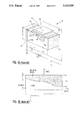
- FIG. 1A shows a representative three-dimensional cross sectional view of a prior art MESFET 50. The channel is normally off, preventing current flow. When a bias is applied to the gate 52, a depletion layer 54, which controls current flow, is modulated in the intrinsic channel (directly under the gate).
- Extrinsic channel 56 which separates the intrinsic channel from the device's source 58 and drain 60 is a source of channel resistance.
- MESFETs and JFETs require an extrinsic channel 56 to prevent drain 60 to gate 52 punchthrough and, to a lesser extent to prevent source 58 to gate 52 punchthrough.
- MESFET drive capability, output power, switching speed and gain are directly affected by both extrinsic and intrinsic channel resistance.
- scaling reduces circuit loads and, for JFETs and MESFETs, device capacitances and channel lengths. For prior art MESFETs and JFETs, this scaling led to first order performance improvements.
- V t threshold voltage
- V bi is the built-in potential of the metal-semiconductor junction
- V p is the pinchoff voltage defined by:
- One prior art approach to reducing the short-channel effects is to increase the impurity (dopant) concentration in the channel.
- Most prior art Si or GaAs FETs have a uniform, lateral doping concentration, i.e., in the x and z direction.
- the dopant level N d has a Gaussian distribution as a function of depth (in the y direction).
- These prior art devices have a high transconductance near pinchoff, and have less device related noise.
- the channel doping has a single discontinuity at some point in the channel, but the dopant level still varies with depth on each side of the discontinuity.
- Increasing channel dopant decreases free carrier mobility and device pinchoff voltage (V p ). Further increasing dopant concentration enhances leakage current and impairs device transconductance.
- a broad-beam ion implantation technique is used to control the active channel doping in MESFET devices. Higher dose implants form source and drain regions with some separation from the gate. Broad beam ion implantation provides a dopant density N d (y) defined by:
- N do is the peak of a doping profile
- y n is the distance of the peak from the top surface
- ⁇ n is the standard deviation (the straggle) of the implanted impurities
- y is the depth of the doping profile below the metal/silicon interface at the gate.
- the preferred embodiment of the present invention is a superlattice heterojunction Field Effect Transistor (FET) that may be a Metal Semiconductor FET (MESFET), or, alternatively, a Junction FET (JFET) with a multi-region channel on a semi-insulating substrate.
- FET Field Effect Transistor
- the multi-region channel has: A first region of Si that extends from the FET's source to a point under the FET's gate, beyond the gate's midpoint; a second region extending from the first region to the FET's drain, comprised of a superlattice of alternating Si and SiGe; and, a semi-insulating region of semi-insulating material extending under the first two regions from the source to the drain.
- FIG. 1A-B illustrates a three-dimensional structure of the prior art of a MESFET.
- FIG. 2 illustrates cross-sectional view of a MESFET according to a preferred embodiment of the present invention.
- FIG. 3A-B represent steps of fabricating a MESFET according to a first preferred embodiment of the present invention.
- FIG. 4 illustrates an elevated view of a superlattice grown for a MESFET according to the first preferred embodiment of the present invention.
- FIG. 5 is a band diagram of a Si/Si 1-x Ge x heterostructure of a superlattice grown according to the first preferred embodiment of the present invention.
- FIG. 6 illustrates a lateral variation of the doping density according to the present invention.
- FIG. 7A-D illustrate a layer structure grown according to a second preferred embodiment of the present invention.
- FIG. 2 illustrates the cross-sectional representation of a MESFET according to a preferred embodiment of the present invention. While the present invention is described in terms of a MESFET, it is contemplated that disclosed device structure and process can be applied to JFETs.
- the MESFET 100 has an N ++ source region 102 and an N ++ drain region 104. Both regions 102, 104 are formed by ion implanting N type dopant into a first semiconductor layer 110. An N type multi-region channel 106 is between the source region 102 and the drain region 104.
- the channel 106 has three regions: First 106A on the left side of dotted line AB and above dotted line CD; Second 106B is on the right side of dotted line AB, and above dotted line CD; and third 106C below dotted line CD.
- the first region 106A is of a first semiconductor material (Si) and extends from the source 102 to dotted line AB, and preferably, includes the larger part of the channel 106 under the gate 108.
- This region 106A is preferably, non-uniformly doped in two dimensions, with N type dopant.
- the second region 106B is adjacent to the first region 106A at dotted line AB and lies between 106A and the drain region 104.
- This second channel region 106B is, preferably, smaller than first channel region 106A, and is a superlattice of quantum wells of Si and a second semiconductor material, Si 1-x Ge x (where x is the Germanium mole fraction in SiGe).
- the third region 106C is a semi-insulating layer, which preferably may be of sapphire or, alternatively, of SiO 2 or very lightly doped N-type Si (hereinafter i-type region).
- Each of the source region 102, gate 108, and the drain region 104 have an electrical contact 114, 116, and 118, respectively.
- FIG. 3A-B show the processing steps of a first preferred embodiment of the present invention.
- An N-type silicon layer 120 is grown on a P silicon substrate 122 either by a Molecular Beam Epitaxy (MBE) method or by a Metal Organic Chemical Vapor Deposition (MOCVD) method.
- the substrate 122 has high resistivity to minimize parasitic substrate effects.
- N type silicon layer 120 is between 0.2 and 0.6 ⁇ m, with a doping density between 1*10 16 and 5*10 16 cm -3 .
- a trench 124 is formed in the surface 126 of the N silicon layer.
- the surface 126 is anisotropically etched using a mixture of CF 4 +O 2 and RIE process.
- a thin thermal oxide is formed on surface 126 and selectively wet etched from the trench with BHF or, alternatively, HF, leaving the trench surfaces relatively clean and the bottom trench surface 127 is uniform (preferably planar).
- the trench is etched through the silicon layer 120.
- the trench 124 is etched to the device's channel depth. For a short-channel MESFET with a submicron channel length (e.g., 0.1 to 0.6 ⁇ m), the desired trench depth is between 0.1 and 0.3 ⁇ m.
- the trench width is kept small for the construction of a short-channel MESFET.
- a superlattice region 128 in FIG. 3B is grown in the trench 124 to form 106B.
- FIG. 4 is a representation of the superlattice structure 128 of channel region 106B, wherein five superlattice periods of Si/Si 1-x G x 130 are selectively grown in the trench 124 to result in a 1 ⁇ device. Fewer periods may be used for shorter channel devices.
- the layers are grown at an epitaxy temperature of about 600° C. on the ⁇ 100 ⁇ -plane of the N silicon.
- the layer sequence of the superlattice 128 is alternating Si 1-x Ge x layers, 132, 134, 136, 138, 140 each about 200 ⁇ thick, and undoped (intrinsic) silicon layers 142, 144, 146, 148, 150 each between 300 and 1000 ⁇ thick.
- FIG. 5 is the energy band diagram of a Si/Si 1-x Ge x heterostructure layer 130.
- a 2-Dimensional Electron Gas (2-DEG) is formed in the undoped silicon side of the hetero-interface of the doped Si 1-x Ge.sub. x 152 and undoped silicon 154.
- Each of Si 1-x Ge x layers 132, 134, 136, 138 and 140 has two sub layers.
- Two-dimensional quantum wells are formed by the heterojunctions at each interface, 132-142, 134-144, 136-146, 138-148, and 140-150.
- the Germanium mole fraction in Si 1-x Ge x directly influences the height of the quantum wells.
- the mole fraction of Ge is preferably 0.5 in the doped sub-layers of the Si 1-x Ge x and, is chosen to maximize the depth of the quantum well without causing structural dislocation of the superlattice layers.
- a smaller mole fraction, x, of Si 1-x Ge x may be substituted to increase the layers' defect-free thickness.
- Preferred embodiment devices have improved electrical performance because they have a high doping density in the channel area 106A and a lower doping density in channel area 106B.
- the source region 102 and the channel region 106A of preferred embodiment devices are non-uniformly doped with a focussed ion beam implantation technique.
- the implant dose is controlled such that besides varying in the y direction as in prior art devices, the doping profile is stepwise varying, with at least 1 step and preferably 5 discrete steps in the x-direction from the source 102, through channel region 106A to the edge of channel region 106B as shown in FIG. 6.
- N do is no longer a constant (horizontally), but a function of x. Consequently, the doping density for the preferred embodiment device, N d (x,y) is defined by:
- channel doping varies in Gaussian fashion with y at each value of x.
- the dopant concentration precisely varies with position and magnitude in a single mask step.
- the preferred embodiment device's vertical and lateral doping profiles are simultaneously varied in a single mask step.
- ohmic contacts are formed by a conventional method for source, gate and drain contacts.
- ohmic contacts are formed by thermal evaporation of 0.3 ⁇ m AuSb with the excess material lifted off of the area surrounding the contacts.
- precautions must be taken to avoid altering the channel dopant density during gate contact metal deposition.
- the gate electrode contacting the topmost layer of the Si/Si 1-x Ge x superlattice 150, undoped or lightly doped silicon should not alter that layer's dopant level.
- This top Superlattice layer 150 in contact with the metal forms a Schottky barrier.
- the structure is annealed at 330° C. under protective gas for 30 seconds.
- the multiple quantum wells of the preferred embodiment device create potential notches at the Si/Si 1-x Ge x interfaces. These potential notches, which contain 2-DEG, extend through the heterostructure region and, therefore, behave as low-resistive paths to the drain. Electrons moving through these notches have a higher mobility because scattering is minimized. This higher mobility reduces carrier transit time and delay occurring through 106B, further improving device performance.
- the dopant level in channel region 106A is higher than the dopant level in channel regions 106B and 106C. Because the dopant density in channel region 106A is not uniform, but lower near the gate, the gate to source capacitance is reduced. However, gate to source breakdown voltage is still high enough for effective device operation. In the superlattices of region 106B, the highly doped Si 1-x Ge x layers 132-140 are much thinner than the undoped silicon layers 142-150 to minimize lattice mismatch structural dislocations.
- the extrinsic channel resistance at the drain is significantly reduced over prior art MESFETs and JFETs and device transconductance is increased without a corresponding decrease in gain or output power.
- the average channel dopant density N d is reduced over prior art devices and junction capacitance is low.
- the preferred embodiment device with two-dimensional graded doping has: N do higher (about 5-8*10 18 cm -3 ) at the source, decreasing in a stepwise fashion to 3-5*10 17 cm -3 at the superlattice edge (see FIG. 6); and, a built-in electrostatic field that accelerates electrons from the source region to the active channel region under the gate, effectively providing increased electron mobility.
- carrier transit time is improved with a corresponding device performance.
- the introduction of a semi-insulating or a lightly doped i-layer between the channel and the substrate significantly reduces the MESFET's gate-substrate junction capacitance.
- the MESFET of the preferred embodiment has an increased frequency response, both because of improved channel transit time and because of reduced device capacitance.
- the hetero-structure is formed by growing superlattice layers, which are sub-etched, and then, using a low temperature lateral overgrowth technique, the sub-etched areas are filled with silicon.
- a technique is disclosed in Burghartz et al., "Self-aligned bipolar epitaxial base n-p-n transistors by selective epitaxy emitter window (SEEW) technology," IEEE Trans. Electron Devices, vol. ED-38, pp. 378-385 (1991).
- FIG. 7A-D illustrate the processing steps of this second preferred embodiment Si/Si 1-x Ge x superlattice N channel MESFET.
- an N type silicon layer 202 is MBE or MOCVD grown on a semi-insulating substrate 204.
- the substrate 204 and the N type silicon layer 202 are identical with the substrate 122 and N type silicon layer 120 of FIG. 3A.
- Five superlattice 208 periods 206 of Si/Si 1-x Ge x are grown on N type silicon layer 202.
- Each superlattice period 206 has an undoped silicon layer 210, 212, 214, 216 and 218 grown on a Si 1-x Ge x layer 220, 222, 224, 226, and 228 respectively.
- the thicknesses and doping characteristics of the layers 210-218 and 220-228 are identical with those of the layers 142-150 and 132-140 respectively.
- the device's source-channel (S-C) and drain regions are defined.
- the drain region is defined when a first portion, 230 in FIG. 7B, is dry etched from the superlattice 208, using a chlorine based etchant on the Si layers to minimize thermal exposure of Si 1-x Ge x , and, using an SF 6 and CF 3 Br plasma for the Si 1-x Ge x layer.
- the etched area is filled with N silicon such that the top surface of the N silicon 240 is co-planar with the unetched top superlattice layer.
- the S-C region 250 is similarly defined, as represented in FIG. 7D, by etching a second superlattice portion.
- the structure of this second preferred embodiment once the S-C region has been defined, is identical with the structure of the first preferred embodiment in FIG. 3B. Further processing of the second preferred embodiment MESFET is identical to that of the first.
Landscapes
- Junction Field-Effect Transistors (AREA)
Priority Applications (4)
| Application Number | Priority Date | Filing Date | Title |
|---|---|---|---|
| US07/995,459 US5323020A (en) | 1992-12-22 | 1992-12-22 | High performance MESFET with multiple quantum wells |
| JP5260052A JP2504376B2 (ja) | 1992-12-22 | 1993-10-18 | 電界効果型トランジスタ |
| EP93480207A EP0607729A3 (fr) | 1992-12-22 | 1993-12-03 | MESFET haute perfomance avec puits quantiques multiples. |
| US08/198,938 US5420059A (en) | 1992-12-22 | 1994-02-18 | Method of making a high performance MESFET with multiple quantum wells |
Applications Claiming Priority (1)
| Application Number | Priority Date | Filing Date | Title |
|---|---|---|---|
| US07/995,459 US5323020A (en) | 1992-12-22 | 1992-12-22 | High performance MESFET with multiple quantum wells |
Related Child Applications (1)
| Application Number | Title | Priority Date | Filing Date |
|---|---|---|---|
| US08/198,938 Division US5420059A (en) | 1992-12-22 | 1994-02-18 | Method of making a high performance MESFET with multiple quantum wells |
Publications (1)
| Publication Number | Publication Date |
|---|---|
| US5323020A true US5323020A (en) | 1994-06-21 |
Family
ID=25541833
Family Applications (2)
| Application Number | Title | Priority Date | Filing Date |
|---|---|---|---|
| US07/995,459 Expired - Lifetime US5323020A (en) | 1992-12-22 | 1992-12-22 | High performance MESFET with multiple quantum wells |
| US08/198,938 Expired - Lifetime US5420059A (en) | 1992-12-22 | 1994-02-18 | Method of making a high performance MESFET with multiple quantum wells |
Family Applications After (1)
| Application Number | Title | Priority Date | Filing Date |
|---|---|---|---|
| US08/198,938 Expired - Lifetime US5420059A (en) | 1992-12-22 | 1994-02-18 | Method of making a high performance MESFET with multiple quantum wells |
Country Status (3)
| Country | Link |
|---|---|
| US (2) | US5323020A (fr) |
| EP (1) | EP0607729A3 (fr) |
| JP (1) | JP2504376B2 (fr) |
Cited By (16)
| Publication number | Priority date | Publication date | Assignee | Title |
|---|---|---|---|---|
| US5500391A (en) * | 1994-08-09 | 1996-03-19 | At&T Corp. | Method for making a semiconductor device including diffusion control |
| US5665981A (en) * | 1994-10-24 | 1997-09-09 | Micron Technology, Inc. | Thin film transistors and method of promoting large crystal grain size in the formation of polycrystalline silicon alloy thin films |
| FR2766619A1 (fr) * | 1997-04-25 | 1999-01-29 | Daimler Benz Ag | Transistors a effet de champ a heterostructure a efficacite de modulation elevee |
| US6229177B1 (en) * | 1998-03-30 | 2001-05-08 | Advanced Micro Devices, Inc. | Semiconductor with laterally non-uniform channel doping profile |
| US6355963B1 (en) * | 1994-11-16 | 2002-03-12 | Matsushita Electric Industrial Co., Ltd. | MOS type semiconductor device having an impurity diffusion layer |
| US20060138581A1 (en) * | 2004-12-23 | 2006-06-29 | Micron Technology, Inc. | Split transfer gate for dark current suppression in an imager pixel |
| US7224007B1 (en) * | 2004-01-12 | 2007-05-29 | Advanced Micro Devices, Inc. | Multi-channel transistor with tunable hot carrier effect |
| US20100052015A1 (en) * | 2008-08-26 | 2010-03-04 | Sanken Electric Co., Ltd. | Semiconductor device |
| US20100123203A1 (en) * | 2008-11-18 | 2010-05-20 | Krishna Kumar Bhuwalka | Tunnel Field-Effect Transistor with Metal Source |
| US20100276732A1 (en) * | 2007-12-26 | 2010-11-04 | Yuji Ando | Semiconductor device |
| US20110027959A1 (en) * | 2008-09-05 | 2011-02-03 | Taiwan Semiconductor Manufacturing Company, Ltd. | Tunnel Field-Effect Transistors with Superlattice Channels |
| US8697510B2 (en) | 2007-07-25 | 2014-04-15 | Taiwan Semiconductor Manufacturing Company, Ltd. | Tunnel field-effect transistor with narrow band-gap channel and strong gate coupling |
| WO2015114482A1 (fr) * | 2014-01-29 | 2015-08-06 | International Business Machines Corporation | Dispositif à semi-conducteur comprenant une ailette à base de silicium-germanium/silicium présentant une structure en super-réseau |
| US9790085B1 (en) * | 2016-06-16 | 2017-10-17 | Nxp Usa, Inc. | Actively preventing charge induced leakage of semiconductor devices |
| US10797137B2 (en) * | 2017-06-30 | 2020-10-06 | Taiwan Semiconductor Manufacturing Co., Ltd. | Method for reducing Schottky barrier height and semiconductor device with reduced Schottky barrier height |
| US11121254B2 (en) * | 2019-08-19 | 2021-09-14 | United Microelectronics Corp. | Transistor with strained superlattice as source/drain region |
Families Citing this family (5)
| Publication number | Priority date | Publication date | Assignee | Title |
|---|---|---|---|---|
| US5753545A (en) * | 1994-12-01 | 1998-05-19 | Hughes Electronics Corporation | Effective constant doping in a graded compositional alloy |
| US6873362B1 (en) * | 1995-03-22 | 2005-03-29 | Sony Corporation | Scanning switch transistor for solid-state imaging device |
| US6399970B2 (en) | 1996-09-17 | 2002-06-04 | Matsushita Electric Industrial Co., Ltd. | FET having a Si/SiGeC heterojunction channel |
| KR100451039B1 (ko) * | 2000-12-20 | 2004-10-02 | 주식회사 하이닉스반도체 | 반도체 소자의 게이트 전극 방법 |
| JP2005319895A (ja) | 2004-05-10 | 2005-11-17 | Kawasaki Heavy Ind Ltd | 立ち乗り型の小型滑走艇 |
Citations (3)
| Publication number | Priority date | Publication date | Assignee | Title |
|---|---|---|---|---|
| US4163237A (en) * | 1978-04-24 | 1979-07-31 | Bell Telephone Laboratories, Incorporated | High mobility multilayered heterojunction devices employing modulated doping |
| US4673959A (en) * | 1983-12-28 | 1987-06-16 | Hitachi, Ltd. | Heterojunction FET with doubly-doped channel |
| US4879256A (en) * | 1985-06-05 | 1989-11-07 | At&T Bell Laboratories | Method of controlling the order-disorder state in a semiconductor device |
Family Cites Families (22)
| Publication number | Priority date | Publication date | Assignee | Title |
|---|---|---|---|---|
| US4261771A (en) * | 1979-10-31 | 1981-04-14 | Bell Telephone Laboratories, Incorporated | Method of fabricating periodic monolayer semiconductor structures by molecular beam epitaxy |
| JPS59181069A (ja) * | 1983-03-30 | 1984-10-15 | Fujitsu Ltd | 半導体装置 |
| JPS6052062A (ja) * | 1983-08-31 | 1985-03-23 | Nec Corp | 電界効果トランジスタ |
| DE3480631D1 (de) * | 1983-06-24 | 1990-01-04 | Nec Corp | Halbleiterstruktur mit uebergitter hoher traegerdichte. |
| JPS6317562A (ja) * | 1986-07-10 | 1988-01-25 | Toshiba Corp | 超格子素子及びその製造方法 |
| US4908678A (en) * | 1986-10-08 | 1990-03-13 | Semiconductor Energy Laboratory Co., Ltd. | FET with a super lattice channel |
| US4999682A (en) * | 1987-08-14 | 1991-03-12 | Regents Of The University Of Minnesota | Electronic and optoelectronic laser devices utilizing light hole properties |
| JPS6481274A (en) * | 1987-09-22 | 1989-03-27 | Matsushita Electric Industrial Co Ltd | Semiconductor device |
| US4863877A (en) * | 1987-11-13 | 1989-09-05 | Kopin Corporation | Ion implantation and annealing of compound semiconductor layers |
| US4839310A (en) * | 1988-01-27 | 1989-06-13 | Massachusetts Institute Of Technology | High mobility transistor with opposed-gates |
| JPH01243591A (ja) * | 1988-03-25 | 1989-09-28 | Hitachi Ltd | 半導体デバイス |
| US5104823A (en) * | 1988-03-31 | 1992-04-14 | Northern Telecom Limited | Monolithic integration of optoelectronic and electronic devices |
| JPH02205325A (ja) * | 1989-02-03 | 1990-08-15 | Sharp Corp | 半導体装置 |
| DE69030129T2 (de) * | 1989-04-12 | 1997-10-09 | Sumitomo Electric Industries | Herstellungsverfahren einer integrierten Halbleiterschaltung |
| JP3194941B2 (ja) * | 1990-03-19 | 2001-08-06 | 富士通株式会社 | 半導体装置 |
| JP2855775B2 (ja) * | 1990-04-20 | 1999-02-10 | 日本電気株式会社 | 電界効果トランジスタ |
| US5266506A (en) * | 1990-07-31 | 1993-11-30 | At&T Bell Laboratories | Method of making substantially linear field-effect transistor |
| US5155571A (en) * | 1990-08-06 | 1992-10-13 | The Regents Of The University Of California | Complementary field effect transistors having strained superlattice structure |
| US5081511A (en) * | 1990-09-06 | 1992-01-14 | Motorola, Inc. | Heterojunction field effect transistor with monolayers in channel region |
| US5104824A (en) * | 1990-11-06 | 1992-04-14 | Bell Communications Research, Inc. | Selective area regrowth for surface-emitting lasers and other sharp features |
| US5142349A (en) * | 1991-07-01 | 1992-08-25 | Motorola, Inc. | Self-doped high performance complementary heterojunction field effect transistor |
| US5219772A (en) * | 1991-08-15 | 1993-06-15 | At&T Bell Laboratories | Method for making field effect devices with ultra-short gates |
-
1992
- 1992-12-22 US US07/995,459 patent/US5323020A/en not_active Expired - Lifetime
-
1993
- 1993-10-18 JP JP5260052A patent/JP2504376B2/ja not_active Expired - Lifetime
- 1993-12-03 EP EP93480207A patent/EP0607729A3/fr not_active Withdrawn
-
1994
- 1994-02-18 US US08/198,938 patent/US5420059A/en not_active Expired - Lifetime
Patent Citations (3)
| Publication number | Priority date | Publication date | Assignee | Title |
|---|---|---|---|---|
| US4163237A (en) * | 1978-04-24 | 1979-07-31 | Bell Telephone Laboratories, Incorporated | High mobility multilayered heterojunction devices employing modulated doping |
| US4673959A (en) * | 1983-12-28 | 1987-06-16 | Hitachi, Ltd. | Heterojunction FET with doubly-doped channel |
| US4879256A (en) * | 1985-06-05 | 1989-11-07 | At&T Bell Laboratories | Method of controlling the order-disorder state in a semiconductor device |
Non-Patent Citations (6)
| Title |
|---|
| A. F. Evason, et al., "Fabrication and Performance of GaAs MESFET's With Graded Channel Doping Using Focused Ion-Beam Implantation" IEEE Electron Device Letters, vol. 9, No. 6, pp. 281-283, Jun. 1988. |
| A. F. Evason, et al., Fabrication and Performance of GaAs MESFET s With Graded Channel Doping Using Focused Ion Beam Implantation IEEE Electron Device Letters, vol. 9, No. 6, pp. 281 283, Jun. 1988. * |
| P. C. Chao, et al., "Channel-Length Effects in Quarter-Micrometer Gate-Length GaAs MESFET's" IEEE Electron Device Letters, vol. EDL-4, No. 9, pp. 326-328, Sep. 1983. |
| P. C. Chao, et al., "Experimental Comparisons in the Electrical Performance of Long and Ultrashort Gate Length GaAs MESFET's" IEEE Electron Device Letters, vol. EDL-3, No. 8, pp. 187-283, Aug. 1982. |
| P. C. Chao, et al., Channel Length Effects in Quarter Micrometer Gate Length GaAs MESFET s IEEE Electron Device Letters, vol. EDL 4, No. 9, pp. 326 328, Sep. 1983. * |
| P. C. Chao, et al., Experimental Comparisons in the Electrical Performance of Long and Ultrashort Gate Length GaAs MESFET s IEEE Electron Device Letters, vol. EDL 3, No. 8, pp. 187 283, Aug. 1982. * |
Cited By (29)
| Publication number | Priority date | Publication date | Assignee | Title |
|---|---|---|---|---|
| US5500391A (en) * | 1994-08-09 | 1996-03-19 | At&T Corp. | Method for making a semiconductor device including diffusion control |
| US5665981A (en) * | 1994-10-24 | 1997-09-09 | Micron Technology, Inc. | Thin film transistors and method of promoting large crystal grain size in the formation of polycrystalline silicon alloy thin films |
| US5977560A (en) * | 1994-10-24 | 1999-11-02 | Micron Technology, Inc. | Thin film transistor constructions with polycrystalline silicon-germanium alloy doped with carbon in the channel region |
| US5985703A (en) * | 1994-10-24 | 1999-11-16 | Banerjee; Sanjay | Method of making thin film transistors |
| US6320202B1 (en) | 1994-10-24 | 2001-11-20 | Micron Technology, Inc. | Bottom-gated thin film transistors comprising germanium in a channel region |
| US6355963B1 (en) * | 1994-11-16 | 2002-03-12 | Matsushita Electric Industrial Co., Ltd. | MOS type semiconductor device having an impurity diffusion layer |
| FR2766619A1 (fr) * | 1997-04-25 | 1999-01-29 | Daimler Benz Ag | Transistors a effet de champ a heterostructure a efficacite de modulation elevee |
| US6229177B1 (en) * | 1998-03-30 | 2001-05-08 | Advanced Micro Devices, Inc. | Semiconductor with laterally non-uniform channel doping profile |
| US7224007B1 (en) * | 2004-01-12 | 2007-05-29 | Advanced Micro Devices, Inc. | Multi-channel transistor with tunable hot carrier effect |
| US7696597B2 (en) | 2004-12-23 | 2010-04-13 | Aptina Imaging Corporation | Split transfer gate for dark current suppression in an imager pixel |
| US20060138581A1 (en) * | 2004-12-23 | 2006-06-29 | Micron Technology, Inc. | Split transfer gate for dark current suppression in an imager pixel |
| US7642107B2 (en) | 2004-12-23 | 2010-01-05 | Aptina Imaging Corporation | Split transfer gate for dark current suppression an imager pixel |
| US7663167B2 (en) * | 2004-12-23 | 2010-02-16 | Aptina Imaging Corp. | Split transfer gate for dark current suppression in an imager pixel |
| US20070102781A1 (en) * | 2004-12-23 | 2007-05-10 | John Ladd | Split transfer gate for dark current suppression an imager pixel |
| US8697510B2 (en) | 2007-07-25 | 2014-04-15 | Taiwan Semiconductor Manufacturing Company, Ltd. | Tunnel field-effect transistor with narrow band-gap channel and strong gate coupling |
| US8344422B2 (en) * | 2007-12-26 | 2013-01-01 | Nec Corporation | Semiconductor device |
| US20100276732A1 (en) * | 2007-12-26 | 2010-11-04 | Yuji Ando | Semiconductor device |
| US20100052015A1 (en) * | 2008-08-26 | 2010-03-04 | Sanken Electric Co., Ltd. | Semiconductor device |
| US8159004B2 (en) * | 2008-08-26 | 2012-04-17 | Sanken Electric Co., Ltd. | Compound semiconductor device having dopant concentration gradient |
| US8669163B2 (en) | 2008-09-05 | 2014-03-11 | Taiwan Semiconductor Manufacturing Company, Ltd. | Tunnel field-effect transistors with superlattice channels |
| US20110027959A1 (en) * | 2008-09-05 | 2011-02-03 | Taiwan Semiconductor Manufacturing Company, Ltd. | Tunnel Field-Effect Transistors with Superlattice Channels |
| US8587075B2 (en) | 2008-11-18 | 2013-11-19 | Taiwan Semiconductor Manufacturing Company, Ltd. | Tunnel field-effect transistor with metal source |
| US20100123203A1 (en) * | 2008-11-18 | 2010-05-20 | Krishna Kumar Bhuwalka | Tunnel Field-Effect Transistor with Metal Source |
| WO2015114482A1 (fr) * | 2014-01-29 | 2015-08-06 | International Business Machines Corporation | Dispositif à semi-conducteur comprenant une ailette à base de silicium-germanium/silicium présentant une structure en super-réseau |
| US9790085B1 (en) * | 2016-06-16 | 2017-10-17 | Nxp Usa, Inc. | Actively preventing charge induced leakage of semiconductor devices |
| US10797137B2 (en) * | 2017-06-30 | 2020-10-06 | Taiwan Semiconductor Manufacturing Co., Ltd. | Method for reducing Schottky barrier height and semiconductor device with reduced Schottky barrier height |
| US11502174B2 (en) | 2017-06-30 | 2022-11-15 | Taiwan Semiconductor Manufacturing Co., Ltd. | Method for reducing Schottky barrier height and semiconductor device with reduced Schottky barrier height |
| US11817481B2 (en) | 2017-06-30 | 2023-11-14 | Taiwan Semiconductor Manufacturing Company, Ltd. | Method for reducing Schottky barrier height and semiconductor device with reduced Schottky barrier height |
| US11121254B2 (en) * | 2019-08-19 | 2021-09-14 | United Microelectronics Corp. | Transistor with strained superlattice as source/drain region |
Also Published As
| Publication number | Publication date |
|---|---|
| EP0607729A3 (fr) | 1995-02-22 |
| JPH07211891A (ja) | 1995-08-11 |
| EP0607729A2 (fr) | 1994-07-27 |
| JP2504376B2 (ja) | 1996-06-05 |
| US5420059A (en) | 1995-05-30 |
Similar Documents
| Publication | Publication Date | Title |
|---|---|---|
| US5323020A (en) | High performance MESFET with multiple quantum wells | |
| US4641161A (en) | Heterojunction device | |
| US4471366A (en) | Field effect transistor with high cut-off frequency and process for forming same | |
| US4916498A (en) | High electron mobility power transistor | |
| WO1989007333A1 (fr) | Dispositif a transistors verticaux fabrique avec post-croissance de semi-conducteurs | |
| US4908325A (en) | Method of making heterojunction transistors with wide band-gap stop etch layer | |
| US5488237A (en) | Semiconductor device with delta-doped layer in channel region | |
| EP0566591B1 (fr) | Dispositif semi-conducteur | |
| WO1988003328A1 (fr) | Transistor a canaux rayes et procede de formation | |
| EP0201873A2 (fr) | Procédé de fabrication d'un transistor à effet de champ métal-semi-conducteur et transistor ainsi obtenu | |
| JP3262056B2 (ja) | バイポーラトランジスタとその製造方法 | |
| JP3127874B2 (ja) | 電界効果トランジスタ及びその製造方法 | |
| US5276340A (en) | Semiconductor integrated circuit having a reduced side gate effect | |
| EP0613189A2 (fr) | Structure de canal de transistor à effet de champ et sa méthode de fabrication | |
| US5552330A (en) | Resonant tunneling fet and methods of fabrication | |
| US5877047A (en) | Lateral gate, vertical drift region transistor | |
| US5381027A (en) | Semiconductor device having a heterojunction and a two dimensional gas as an active layer | |
| US4994868A (en) | Heterojunction confined channel FET | |
| US5258631A (en) | Semiconductor device having a two-dimensional electron gas as an active layer | |
| US4962050A (en) | GaAs FET manufacturing process employing channel confining layers | |
| KR100563884B1 (ko) | 접합형 전계 효과 트랜지스터의 제조 방법 | |
| KR100752538B1 (ko) | 바이폴라 트랜지스터 | |
| EP0469768A1 (fr) | Transistor à effet de champ linéaire en substance et procédé pour sa fabrication | |
| GB2239557A (en) | High electron mobility transistors | |
| JP2643890B2 (ja) | トンネルトランジスタ |
Legal Events
| Date | Code | Title | Description |
|---|---|---|---|
| AS | Assignment |
Owner name: INTERNATIONAL BUSINESS MACHINES CORPORATION, NEW Y Free format text: ASSIGNMENT OF ASSIGNORS INTEREST;ASSIGNORS:MOHAMMAD, S. NOOR;RENBECK, ROBERT B.;REEL/FRAME:006600/0081 Effective date: 19921221 |
|
| STCF | Information on status: patent grant |
Free format text: PATENTED CASE |
|
| CC | Certificate of correction | ||
| FPAY | Fee payment |
Year of fee payment: 4 |
|
| FPAY | Fee payment |
Year of fee payment: 8 |
|
| FPAY | Fee payment |
Year of fee payment: 12 |