US5401357A - Dry etching method - Google Patents
Dry etching method Download PDFInfo
- Publication number
- US5401357A US5401357A US07/937,781 US93778192A US5401357A US 5401357 A US5401357 A US 5401357A US 93778192 A US93778192 A US 93778192A US 5401357 A US5401357 A US 5401357A
- Authority
- US
- United States
- Prior art keywords
- etching
- gaas
- dry etching
- light
- region
- Prior art date
- Legal status (The legal status is an assumption and is not a legal conclusion. Google has not performed a legal analysis and makes no representation as to the accuracy of the status listed.)
- Expired - Fee Related
Links
Images


Classifications
-
- H—ELECTRICITY
- H10—SEMICONDUCTOR DEVICES; ELECTRIC SOLID-STATE DEVICES NOT OTHERWISE PROVIDED FOR
- H10P—GENERIC PROCESSES OR APPARATUS FOR THE MANUFACTURE OR TREATMENT OF DEVICES COVERED BY CLASS H10
- H10P50/00—Etching of wafers, substrates or parts of devices
- H10P50/20—Dry etching; Plasma etching; Reactive-ion etching
- H10P50/24—Dry etching; Plasma etching; Reactive-ion etching of semiconductor materials
- H10P50/246—Dry etching; Plasma etching; Reactive-ion etching of semiconductor materials of Group III-V materials
-
- H—ELECTRICITY
- H10—SEMICONDUCTOR DEVICES; ELECTRIC SOLID-STATE DEVICES NOT OTHERWISE PROVIDED FOR
- H10D—INORGANIC ELECTRIC SEMICONDUCTOR DEVICES
- H10D10/00—Bipolar junction transistors [BJT]
- H10D10/01—Manufacture or treatment
- H10D10/021—Manufacture or treatment of heterojunction BJTs [HBT]
-
- H—ELECTRICITY
- H10—SEMICONDUCTOR DEVICES; ELECTRIC SOLID-STATE DEVICES NOT OTHERWISE PROVIDED FOR
- H10D—INORGANIC ELECTRIC SEMICONDUCTOR DEVICES
- H10D30/00—Field-effect transistors [FET]
- H10D30/01—Manufacture or treatment
- H10D30/015—Manufacture or treatment of FETs having heterojunction interface channels or heterojunction gate electrodes, e.g. HEMT
-
- H—ELECTRICITY
- H10—SEMICONDUCTOR DEVICES; ELECTRIC SOLID-STATE DEVICES NOT OTHERWISE PROVIDED FOR
- H10D—INORGANIC ELECTRIC SEMICONDUCTOR DEVICES
- H10D64/00—Electrodes of devices having potential barriers
- H10D64/01—Manufacture or treatment
- H10D64/012—Manufacture or treatment of electrodes comprising a Schottky barrier to a semiconductor
- H10D64/0124—Manufacture or treatment of electrodes comprising a Schottky barrier to a semiconductor to Group III-V semiconductors
- H10D64/0125—Manufacture or treatment of electrodes comprising a Schottky barrier to a semiconductor to Group III-V semiconductors characterised by the sectional shape, e.g. T or inverted T
-
- H—ELECTRICITY
- H10—SEMICONDUCTOR DEVICES; ELECTRIC SOLID-STATE DEVICES NOT OTHERWISE PROVIDED FOR
- H10P—GENERIC PROCESSES OR APPARATUS FOR THE MANUFACTURE OR TREATMENT OF DEVICES COVERED BY CLASS H10
- H10P14/00—Formation of materials, e.g. in the shape of layers or pillars
- H10P14/60—Formation of materials, e.g. in the shape of layers or pillars of insulating materials
- H10P14/63—Formation of materials, e.g. in the shape of layers or pillars of insulating materials characterised by the formation processes
- H10P14/6302—Non-deposition formation processes
- H10P14/6304—Formation by oxidation, e.g. oxidation of the substrate
- H10P14/6306—Formation by oxidation, e.g. oxidation of the substrate of the semiconductor materials
-
- H—ELECTRICITY
- H10—SEMICONDUCTOR DEVICES; ELECTRIC SOLID-STATE DEVICES NOT OTHERWISE PROVIDED FOR
- H10P—GENERIC PROCESSES OR APPARATUS FOR THE MANUFACTURE OR TREATMENT OF DEVICES COVERED BY CLASS H10
- H10P50/00—Etching of wafers, substrates or parts of devices
- H10P50/69—Etching of wafers, substrates or parts of devices using masks for semiconductor materials
- H10P50/691—Etching of wafers, substrates or parts of devices using masks for semiconductor materials for Group V materials or Group III-V materials
- H10P50/692—Etching of wafers, substrates or parts of devices using masks for semiconductor materials for Group V materials or Group III-V materials characterised by their composition, e.g. multilayer masks or materials
-
- H—ELECTRICITY
- H10—SEMICONDUCTOR DEVICES; ELECTRIC SOLID-STATE DEVICES NOT OTHERWISE PROVIDED FOR
- H10D—INORGANIC ELECTRIC SEMICONDUCTOR DEVICES
- H10D62/00—Semiconductor bodies, or regions thereof, of devices having potential barriers
- H10D62/80—Semiconductor bodies, or regions thereof, of devices having potential barriers characterised by the materials
- H10D62/85—Semiconductor bodies, or regions thereof, of devices having potential barriers characterised by the materials being Group III-V materials, e.g. GaAs
Definitions
- the present invention relates to a dry etching method, and particularly, to a dry etching method capable of selectively etching the desired material from a plurality of materials having different types of band gap energies or from a plurality of materials having different band gap energies.
- the technique of selectively etching the desired material from a plurality of semiconductors having different compositions is very important in fabrication of a compound semiconductor device. For example, in fabrication of a semiconductor device having a heterostructure of GaAs and Al x Ga 1-x As, Al x Ga 1-x As is selectively etched by wet etching and GaAs is selectively etched by dry etching.
- the selective wet etching of Al x Ga 1-x As is conducted using an etchant of HCl/H 2 O 2 or NH 3 /H 2 O 2 /H 2 O. This is utilized in fabrication of a laser diode, HBT(Hetero-Bipolar Transistor) and the like.
- HBT Hetero-Bipolar Transistor
- the wet etching has such a problem as causing an under-cut and is thus unsuitable for fine patterning.
- both the dry and wet etching techniques must be combined.
- wet etching is unsuitable for fine patterning, it is desired to selectively etch GaAs and Al x Ga 1-x As by only dry etching.
- the present invention has been made, and the object is to provide a method for selectively etching Al x Ga 1-x As to GaAs.
- a method for selectively etching Al x Ga 1-x As to GaAs by irradiating a light on a sample to be etched for changing an etching rate ratio between Al x Ga 1-x As and GaAs.
- the present invention has realized the selective etching of Al x Ga 1-x As to GaAs, for example, by utilizing the difference in a photo-absorbing characteristic between Al x Ga 1-x As and GaAs.
- Al x Ga 1-x As is variable in the transition type and the band gap energy Eg (Al x Ga 1-x As) depending on the composition (x).
- FIG. 15 shows a relationship between the composition and the band gap energy. In general, the relationship between the Eg (Al x Ga 1-x As) and Eg (GaAs) is represented as follows:
- GaAs film on GaAs substrate it is possible to promote the film forming reaction through the photo-absorption by a substrate.
- the reason for this is that electrons and positive holes photo-excited on the surface of GaAs react with a source gas molecules absorbed on the surface of GaAs.
- Al x Ga 1-x As has a small photo-absorption coefficient as compared with GaAs, the film formation by the photo-absorption of the substrate is retarded as compared with GaAs.
- a source gas for forming GaAs is introduced into an etching chamber, and a light 4 having such a wavelength as satisfying the above equation (2), that is, capable of being absorbed by only GaAs is irradiated on the sample. Consequently, the etching rate is retarded on the surface of the GaAs 2 because the etching reaction and the film formation due to the photo-CVD reaction of GaAs are competed with each other. Meanwhile, only the etching reaction is progressed on the surface of the Al x Ga 1-x As 1.
- the Al x Ga 1-x As 1 is selectively etched as shown in FIG. 1b, and the etching rate of GaAs is significantly small.
- the portion 5 of GaAs formed by the photo-CVD reaction is emphasized.
- various conditions are adjusted such that the photo-CVD reaction and the etching reaction of GaAs are cancelled to each other so as to generate the least possible film formation and the etching.
- a light as satisfying the above equation (3) that is, capable of being absorbed by Al x Ga 1-x As may be used as an irradiated light.
- the reason for this is that, even in the light having such a wavelength, the photo-absorption coefficient of GaAs is larger than Al x Ga 1-x As.
- the etching reaction tends to be obstructed and retarded by an oxide film formed on the surface of a sample.
- the sticking coefficient of O 2 is made larger several times. This is seemed to be related to the carriers generated on the GaAs surface.
- the oxide film equivalent to one molecular layer is formed on the GaAs surface.
- oxygen other than the etching gas is introduced in the etching chamber, and the etching is conducted by irradiating the light having the wavelength satisfying the equation (2), that is, capable of being absorbed by only GaAs, so that the surface of the GaAs 1 is covered with a thin oxide film for obstructing the etching reaction, resulting in the retarded etching rate.
- the selective etching of the Al x Ga 1-x As 1 is possible to the GaAs 2.
- the photo-stimulated desorption is induced by a thermal mechanism by heating of the substrate, and an electronic mechanism by the electronic kinetics through excitation of electronic state of the absorbing material or the substrate.
- the electronic kinetics through excitation of electronic state of the substrate is related.
- the electrons excited to the empty level above the Fermi energy are elastically tunneled to the empty level of the absorbed gas molecules, which promotes the stimulated desorption of the absorbed molecules. Accordingly, when the etching gas is absorbed and is reacted with the surface, by promotion of the stimulated desorption being reversed to the absorption, the absorbed gas can be desorbed before being reacted with the substrate, resulting in the retarded etching reaction.
- the sample including an Al x Ga 1-x As 1 and a GaAs 2 as shown in FIG. 1a when the light capable of being absorbed by only GaAs is irradiated, the stimulated desorption of the absorbed etching gas is promoted on the GaAs surface thereby reducing the etching rate, which enables the selective etching of Al x Ga 1-x As to GaAs.
- the chemical reaction mainly dominates the dry etching, the utilization of the photo-stimulated desorption is particularly effective.
- a light satisfying the equation (3) that is, capable of being absorbed by Al x Ga 1-x As may be used as the irradiated light. This is because, even in the light having such a wavelength, the photo-absorption coefficient of GaAs is larger than Al x Ga 1-x As.
- the present invention has been explained regarding the selective etching of Al x Ga 1-x As to GaAs, it is applicable for the whole selective etching of the material having the smaller photo-absorption among the materials having different photo-absorption characteristics.
- the types of band gap energies for the main semiconductors are shown in Table 1. By suitable combination of the materials as shown in Table 1, the selective etching is possible by easily applying the present invention.
- the etching in a sample having an composition continuously variable in the thickness direction, that is, a graded composition, the etching can be stopped at the depth having the specified composition.
- the band gap energy of the direct transition is represented in the following equation (6) as a function Eg(x)[eV] of the composition (x) of Al.
- the value of Eg on the surface of the sample becomes smaller gradually.
- the etching may be conducted while irradiating the light having a wavelength ⁇ o represented in the equation (7) on the sample. ##EQU3##
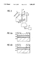
- FIGS. 1a and 1b are views for explaining the principle of the present invention.
- FIG. 2 is a view showing an etching equipment used in Example 1 of the present invention
- FIGS. 3a and 3b are views showing Example 2 of the present invention.
- FIG. 4 is a view showing an etching equipment used in Example 2 of the present invention.
- FIG. 5 is an etching equipment used in Example 3 of the present invention.
- FIGS. 6a and 6b are views showing Example 4 of the present invention.
- FIGS. 7a and 7b are views showing Example 5 of the present invention.
- FIGS. 8a and 8b are views showing Example 6 of the present invention.
- FIG. 9 is a view showing an etching equipment used in Example 6 of the present invention.
- FIG. 10 is a view showing Example 7 of the present invention.
- FIGS. 11a and 11c are views showing Example 8 of the present invention.
- FIGS. 12a and 12c are views showing Example 9 of the present invention.
- FIGS. 13a and 13b are views showing a method for fabricating a recessed gate HEMT of the present invention.
- FIGS. 14a and 14c are views showing Example 10 of the present invention.
- FIG. 15 is a graph showing a relationship between the band gap energy and the composition.
- the photo-CVD reaction is utilized.
- RIE Reactive Ion Etching
- TMGa Ga (CH 3 ) 3 trimethylgallium
- AsH 3 s(arsine) are used as a source gas for forming GaAs
- a low pressure mercury lamp is used as a light source of photo-CVD.
- FIG. 2 An equipment used in this Example is shown in FIG. 2.
- the ground electrode of the conventional RIE equipment is replaced into a meshly ground electrode 8, and a light from a low pressure mercury lamp 6 can be irradiated to a sample 11 through a fused quartz window 7.
- the low pressure mercury lamp 6 emits an ultra-violet light having a wavelength of 185 nm and 245 nm. It is sufficiently shorter than the wavelength of the photon corresponding to the energy of the band gap energy of GaAs or Al x Ga 1-x As. However, the absorption coefficient of GaAs is seemed to be remarkably larger than Al x Ga 1-x As.
- the sample 11 is placed in an etching chamber 9, and the etching chamber 9 is then exhausted at 0.001 m Torr or less by a pumping system 13.
- an etching gas of CCl 4 (at 40 ⁇ m Torr)+He (at 50 ⁇ m Torr), and a source gas of TMGa (at 80 ⁇ m Torr)+sH 3 (at 40 ⁇ m Torr) for forming GaAs are introduced from a gas supply system 10.
- the low pressure mercury lamp 9 is lightened, and the gas in the etching chamber is discharged by a RF power supply 14. Consequently, as shown in FIG. 1b, only the Al x Ga 1-x As 1 is etched to a thickness of approximately 100 nm, and the etching of the GaAs 2 is not recognized.
- the source gas molecules for forming GaAs even in vapor phase by the RF discharge, and thus a thin GaAs film is formed on the whole surface of the substrate.
- the GaAs forming reaction through the light absorbed by the substrate is added thereto on the GaAs 2, so that the thickness of the GaAs film formed on the GaAs 2 is made thicker than the Al x Ga 1-x As 1. Therefore, the etching reaction is not progressed on the GaAs 2 because the GaAs forming reaction is balanced to the etching reaction. Meanwhile, the etching reaction is predominant on the Al x Ga 1-x As 1, and accordingly, the Al x Ga 1-x As 1 is selectively etched.
- the etching of the Al x Ga 1-x As is conducted using the RIE.
- the RIE is an etching technique excellent in anisotropy and suitable for fine patterning.
- the selective etching utilizing the photo-CVD reaction is recognized to be effective to the RIE.
- the photo-oxidation reaction is utilized.
- oxygen is used as an oxidation gas.
- the Cl 2 molecule has an absorption peak near the wavelength of 340 nm
- the XeF excimer laser having the wavelength of 351 or 353 nm is suitable for excitation of Cl 2 .
- An Ar ion laser having the oscillating wavelength of 514.5 nm is used for excitation of the photo-reaction on the GaAs surface.
- FIG. 4 The brief construction of an equipment used in this Example is shown in FIG. 4.
- a laser beam from a XeF excimer 18 is made to horizontally pass over a sample 11 through a fused quartz window 7 for exciting the Cl 2 molecules in a gas phase.
- a light from an Ar ion laser 16 is enlarged by an optical system 17, and is vertically irradiated on the sample 11.
- the sample 11 is obtained by growing an Al x Ga 1-x As film 1 to a thickness of 150 nm on a GaAs substrate 3, and further forming the pattern of a resist film 15 thereon.
- the wavelength corresponding to the band gap energy 2.48 eV of the direct transition of Al x Ga 1-x As is 500 nm, and accordingly, the light of the Ar ion laser is not absorbed by Al x Ga 1-x As as compared with GaAs.
- the etching is conducted in the following manner: The sample 11 is placed in an etching chamber 9, and the etching chamber 9 is then exhausted at 0.001 m Torr or less by a pumping system 13. Subsequently, Cl 2 (at 10 ⁇ m Torr) and oxygen (at 100 ⁇ m Torr) are introduced in the etching chamber 9 by a gas supply system 10. Lights from the Ar ion laser 16 and the XeF excimer laser 18 are irradiated for 30 min. Consequently, as shown in FIG. 3b, an Al x Ga 1-x As film 1 is etched up to the surface of the GaAs substrate 2 according to the pattern of the resist 15. Also, even if the (laser) irradiation is further progressed, the GaAs substrate 2 is little etched.
- the photo-etching reaction of Al x Ga 1-x As is progressed by the Cl 2 photo-excited in the vapor phase, and at the time when the etching reaches the surface of the GaAs substrate 3, the photo-oxidation reaction is generated through the photo-absorption by GaAs, thus forming an oxide film 66 on the surface of the GaAs substrate 3, which obstructs the progress of the etching.
- the etching of the Al x Ga 1-x As is conducted using the photo-etching. This is expected as an effective etching technique because of eliminating the possibility of the damage generated by charged particles and high energy particles in the plasma etching. As shown in this Example, the selective etching technique utilizing the photo-oxidation reaction is recognized to be effective to the photo-etching.
- FIG. 5 The brief construction of an equipment used in this Example is shown in FIG. 5.
- a hot molecular beam generating nozzle 20 is positioned over a sample 11 placed on a substrate holder 19.
- a Cl 2 hot molecular beam 22 is vertically irradiated on the sample 11.
- the light from a low pressure mercury lamp 6 is irradiated obliquely on the sample 11 through a fused quartz window 7.
- the sample 11 is placed in an etching chamber 9, and the etching chamber 9 is exhausted at 0.001 ⁇ m Torr or less.
- the nozzle portion of the hot molecular beam generator 20 is heated at 800° C., and a Cl 2 gas 21 is supplied at an amount of 10 sccm and the Cl 2 hot molecular beam 22 is irradiated on the sample 11.
- a low pressure mercury lamp 6 is lightened. This state is kept for 30 min. and the etching is conducted, and thus only the Al x Ga 1-x As 1 is etched to a thickness of approximately 100 nm as shown in FIG. 1b.
- the etching of the Al x Ga 1-x As is conducted using a hot molecular beam. This is expected as an effective etching technique because of eliminating the possibility of the damage generated by charged particles and/or high energy particles in the plasma. As shown in this Example, the selective etching technique utilizing the photo-stimulated desorption is recognized to be effective to the molecular beam etching.
- the present invention is applied for the selective etching of Si layer to a Si n Ge n (n: number of atomic layers) supper lattice layer.
- Si or Ge is essentially an indirect semiconductor.
- type of transistor is changed into a direct semiconductor.
- the photo-absorption coefficient of the super lattice structure is made larger as compared with that of the original indirect semiconductor. Therefore, it is possible to selectively etch only a Si layer or Ge layer to the super lattice layer according to the present invention.
- an etching equipment as shown in FIG. 4 is used.
- a sample 11 is obtained by 20 layers of Si 4 /Ge 4 super lattice layers 25 and a Si layer 24 on a Si substrate 26 by MBE (Molecular Beam Epitaxy) as shown in FIG. 6.
- the sample 11 is formed with a mask pattern 23 on its surface by photolithography, and is then placed in an etching chamber 9.
- Cl 2 and O 2 are used as an etching gas and an oxidation gas, respectively.
- exhaustion in the etching chamber 9, introduction of the etching gas and oxidation gas, and irradiation of the Ar ion laser beam and XeF excimer laser beam are conducted. Consequently, as shown in FIG. 6b, the etching is stopped at the Si layer of the outermost portion of the super lattice layer 25.
- the surface is examined by an Auger electron spectroscopy method, which shows oxidation of about two atomic layers of Si.
- the present invention is effective for fabrication of the semiconductor device having the Si n Ge n super lattice structure.
- the present invention is applied for the selective etching of the Al x Ga 1-x As emitter layer in a process of exposing a base layer in fabrication of HBT.
- FIG. 7a shows a sectional structure of an ideal HBT.
- n + -GaAs (sub-collector) layer 34 there are sequentially formed n + -GaAs (sub-collector) layer 34, n-GaAs (collector) layer 32, p + -GaAs (base) layer 31, n-Al x Ga 1-x As (emitter) layer 29 and n + -GaAs (cap) layer 28 on a semi-insulated GaAs substrate 35.
- the lithography and etching process are repeated for forming an emitter area, base electrode contact portion and a collector electrode contact portion, and finally an emitter electrode 27, base electrode 30 and collector electrode 33 are formed by a lift-off method.
- the present invention is applied for the etching of the n-Al x Ga 1-x As (emitter) layer 29.
- a wafer is obtained by forming each layer of HBT using a MBE equipment with an ultra-high vacuum, and then forming a resist mask on an emitter area by lithography.
- the wafer is placed in an etching chamber as shown in FIG. 2.
- the usual RIE is conducted using an etching gas of CCl 2 F 2 .
- etching gas of CCl 2 F 2 In this etching, only the n + -GaAs (cap) layer 28 is etched, and thus the surface of n-Al x Ga 1-x As As (emitter) layer 29 is exposed.
- the RIE is conducted using an etching gas of CCl 4 and a source gas of (TMGa+AsH 3 ), and a low pressure mercury lamp as a light source of the photo-CVD.
- a source gas of (TMGa+AsH 3 ) a source gas of (TMGa+AsH 3 )
- a low pressure mercury lamp as a light source of the photo-CVD.
- the wafer is taken-out and formed with a resist mask so as to expose a sub-collector area, after which the p + -GaAs (base) layer 31 and the n-GaAs (collector) layer 32 are etched by the RIE using the etching gas of CCl 4 . Finally, an emitter electrode 27, base electrode 30 and collector electrode 33 are formed by a lift-off method.
- the maximum oscillating frequency f max of the HBT in this Example is made higher (approximately 60 GHz) as compared with the conventional manner (30-50 GHz). Further, the scattering thereof is almost eliminated resulting in the improved characteristics.
- the etching is stopped at the depth of the desired composition.
- the sample used in this Example is shown in FIG. 8a.
- the sample is obtained by forming an Al x Ga 1-x As layer 36 having a graded composition to a thickness of 100 nm on a semi-insulated substrate 35 by a MBE method.
- the composition (x) is set to be 0.3 at the surface and 0.0 at the interface to coincide with the substrate, that is, GaAs.
- the etching is conducted while irradiating a laser beam with a wavelength of 773 nm. This wavelength corresponds to the band gap energy of the composition (x) of the Al x Ga 1-x As in the equation (7) and at the temperature of 300K.
- FIG. 9 An etching equipment used in this Example is shown in FIG. 9. The characteristics of this etching equipment are as follows:
- the light source for inducing the photo-CVD reaction there is used a solid-state tunable laser 37 having a laser crystal of Alexandrite (BeAl 2 O 4 ) and a pumping of a mercury arc lamp. Further, there is used a RF electrode 38 having a heater and a water-cooling mechanism. To stop the etching at the specified composition, it is required to irradiate the light having a wavelength accurately corresponding to the band gap energy at the composition. Also, since the band gap energy is changed depending to the temperature, it also becomes important to keep the substrate temperature at constant.
- the sample 11 is placed in the etching chamber 9, and the etching is conducted in the same manner as in Example 1. Namely, an etching gas (CCl 4 ) and a source gas of GaAs (TMGa+AsH 3 ) are introduced in this order into the etching chamber 9, after which the irradiation of the laser beam from the solid-state tunable laser 37 is started. Finally, the gases in the etching chamber are discharged. The sample is kept at a temperature of 300 ⁇ K.
- the GaAs film on the etched surface is very thin, which can be simply removed by dry etching or wet etching.
- the source gas for CVD may be added with a TMAI(Al(CH 3 ) 3 :trimethylealuminum) as a source gas of aluminum.
- the partial pressures of the TMGa and TMAI are respectively adjusted such that the composition (x) of the Al x Ga 1-x As layer formed by the photo-CVD reaction becomes 0.15.
- the photo-CVD reaction has been used in this Example; however, as shown in the next Example 7 , by using the etching equipment improving that as shown in FIG. 4 wherein the Ar ion laser 16 is replaced into the solid-state tunable laser 37, and the substrate holder 16 includes a heater and cooling mechanism, the present invention utilizing the photo-oxidation reaction can be applicable.
- Example 6 is further developed and the present invention is applicable for fabrication of a HBT having a graded composition base layer.
- FIG. 10 shows a structure of the HBT having the graded composition base layer.
- an electric field is generated in a base region, which accelerates an electron, that is, shortens the base traveling time of the electron thus improving the RF characteristic.
- Example 6 As mentioned in the last of Example 6, there is used the etching equipment improving that as shown in FIG. 4.
- a resist mask is formed on an emitter area by lithography.
- a n + -GaAs (cap) layer 28 is selectively etched by an usual RIE equipment using an etching gas of CCl 2 F 2 so as to expose the surface of a n-Al x Ga 1-x As (emitter) layer 29.
- the wafer is set in an etching chamber 9 of the etching equipment improving that as shown in FIG. 4, and the selective etching of the present invention utilizing the photo-oxidation reaction is conducted.
- the wafer is taken out of the etching chamber 9 and is then formed with a resist mask such that a sub-collector region is exposed.
- the p + -Al x Ga 1-x As (graded composition base) layer 39 and a u-GaAs (collector) layer 40 are respectively etched by the RIE using the etching gas of CCl 4 .
- an emitter electrode 27, base electrode 30 and collector electrode 33 are formed by a known lithography method.
- the HBT having the graded composition formed in this Example has the maximum oscillating frequency of approximately 80 GHz, with little scattering of thereof.
- the present invention is applicable as it is.
- the present invention is applied for checking the thickness of Al x Ga 1-x As crystal growth film.
- the most simple method for measuring the thickness of the crystal growth film is to partially etch the crystal growth film and measure the height of the step by a stylus thickness meter. A plurality of points on the wafer can be measured for a short time by this method. Consequently, this method is suitable for checking the thickness distribution. Since the etching of only the GaAs layer is possible by the conventional dry etching, the thickness of the GaAs film formed on the Al x Ga 1-x As is measured by the above method. In this Example, the Al x Ga 1-x As film can be selectively etched, which makes it possible to measure the thickness distribution of the Al x Ga 1-x As film formed on the GaAs wafer, in contrast with the conventional one.
- FIGS. 11a to 11c show a method for measuring the thickness distribution according to this Example.
- a resist mask 41 is formed on a sample obtained by growing an Al x Ga 1-x As film 42 on a GaAs wafer 43.
- FIG. 1b only the exposed portion of the Al x Ga 1-x As film 42 is etched.
- the resist mask 41 is removed for revealing the step as shown in FIG. 11.
- the step height is measured by the stylus thickness meter, resulting in the obtained thickness distribution.
- the present invention utilizing the photo-CVD reaction is applied for the fabrication process of HIGFET (Heterostructure Insulated Gate Field Effect Transistor).
- HIGFET Heterostructure Insulated Gate Field Effect Transistor
- FIG. 12 shows a sectional structure of the HIGFET having such a feature that a Schottky junction formed between a W/WSi gate 44 and a u-Al 0 .3 Ga0.7As 46 artificially serves as an insulating film.
- the fabricating procedure of the HIGFET is as follows: a GaAs (buffer) layer 54, p-GaAs layer 53, n-GaAs (channel) layer 47 and u-Al 0 .3 Ga 0 .7 As 46 are formed on a semi-insulated GaAs substrate 35 by epitaxial growth.
- the film of each layer and the impurity concentration are shown in Table 2.
- the mesa-etching is conducted on the way of the p-GaAs layer 53. Thereat, there is formed the W/WSi gate 44. Subsequently, there are formed a SiO 2 pattern 52 and a gate electrode side wall SiO 2 film 51. This is shown in FIG. 12b. After masking of the SiO 2 pattern 52 and the gate electrode side wall SiO 2 film 51, the exposed portion of the u-Al 0 .3 Ga 0 .7 As layer 46 is etched. In this Example, the present invention is applied for the etching of the u-Al 0 .3 Ga 0 .7 As layer 46. After that, using MOCVD, a n + -GaAs layer 50 is selectively grown, and the source electrode/drain electrode 49 are respectively formed by a known lift-off method, to thus obtain the HIGFET.
- the etching is not stopped at the surface of the GaAs (channel) layer under the u-Al 0 .3 Ga 0 .7 As layer 46, thus causing the over-etching.
- the over-etching is essential to perfectly remove the u-Al 0 .3 Ga 0 .7 As layer 46.
- the n-GaAs layer (channel) layer 47 is made thinner, and thus the source resistance and drain resistance are increased, which deteriorates the characteristic of the HIGFET.
- only the u-Al 0 .3 Ga 0 .7 As layer 46 is etched, and therefore, there little occurs the over-etching thereby eliminating a fear of causing such a trouble.
- the wafer after completing the processes as shown in FIG. 12b is placed in an etching chamber 9 of the etching equipment as shown in FIG. 9.
- the oscillating wavelength of the solid-state tunable laser 37 is adjusted to be 800 nm.
- the light having such a wavelength is not absorbed by the u-Al 0 .3 Ga 0 .7 As layer 46 but by only the n-GaAs layer (channel) layer 47.
- the etching is conducted in the same procedure as in Example 1, except that in completing the selective etching, the laser beam irradiation from the solid-state tunable laser 37 and the supply of TMGa and AsH 3 are previously stopped and the usual RIE is conducted for 5 min.
- the thin GaAs film formed on the whole surface, for example, on the SiO 2 pattern 52 is removed by discharge in a vapor phase. Consequently, as shown in FIG. 12c, only the u-Al 0 .3 Ga 0 .7 As layer 46 is selectively etched.
- a n + -GaAs layer 50 is re-grown by the MOCVD using a source gas of (TMGa+AsH 3 ) and a doping gas of Si 2 H 6 , and finally the source electrode/drain electrode 49 are respectively formed by the lift-off method, to thus obtain the HIFET.
- the source resistance is 0.5 ⁇ .mm, which is significantly improved as compared with the conventional value of 0.7 ⁇ .mm.
- the present invention is applied for a recessed gate HEMT (High Electron Mobility Transistor).
- FIG. 13 shows a sectional structure of the HEMT.
- the thickness of each layer and the impurity concentration are shown in Table 3.
- the structure of the usual HEMT is shown in FIG. 13a.
- the characteristic of the HEMT device is significantly affected by the resistance of the gap between the gate electrode 45 and the n + -GaAs (cap) layer 28.
- the gap is required to secure the break-down resistance between the gate electrode 45 and the n + -GaAs (cap) layer 28. While the dimension is contracted in the lateral direction in FIG. 13a, the distance of the above gap is usually 100-300 nm, and the depth from the gate electrode 45 to the channel layer is several ten nm.
- the source resistance is dependent on the concentration of the carriers remaining on the channel layer under the above gap portion 63.
- the n-Al 0 .15 Ga 0 .85 As (carrier supply) layer 59 is thinner, which exert a large effect on the device having a low threshold voltage.
- the recessed gate HEMT as shown in FIG. 13b provides the u-GaAs (cover) layer 57 for increasing the carrier concentration. Since the u-GaAs (cover) layer 57 lowers the conduction band energy of the whole heterostructure under the u-GaAs (cover) layer 57, the concentration of the carriers remaining in the u-In x Ga 1-x As (channel) layer 61 is increased, the resistance of the above gap portion is reduced, and the source resistance is reduced. As a result, a mutual conductance gm is enhanced, which makes it possible to improve the characteristics of the device such as a cutoff frequency f t , maximum oscillating frequency f max and noise factor NF.
- the gate portion of the recessed gate HEMT is usually fabricated in the procedure as shown in FIGS. 14a to 14c.
- a SiO 2 film 65 is wet etched using a resist pattern 64 for forming the gate as a mask, and the n + GaAs film 28 being a cap layer is selectively etched by the RIE.
- the u-Al 0 .3 Ga 0 .7 As layer 56 serves to stop the etching.
- the over-etching is conducted, and consequently the etching is progressed in the lateral direction.
- the present invention has been applied for etching the u-Al 0 .3 Ga 0 .7 As (etching stop) layer 56.
- the etching is conducted using the etching equipment as shown in FIG. 9.
- the wavelength of the solid-state tunable laser is adjusted to be 800 nm.
- the wafer completing the wet etching of the SiO 2 film 65 is set in the etching chamber 9, and the n + -GaAs (cap) layer 28 is selectively etched by the RIE using the etching gas of CCl 2 F 2 .
- the etching gas changed into CCl 4 and also a source gas of (TMGa+AsH 3 ) for forming GaAs are introduced, and the u-Al 0 .3 Ga 0 .7 As (cover) layer 56 is selectively etched using the photo-CVD reaction of the present invention.
- the etching gas is changed into CCl 2 F 2 again, and the u-GaAs (cover) layer 58 is selectively etched.
- the etchings are conducted in the different manners: the n + -GaAs (cap) layer 28, RIE; u-Al 0 .3 Ga 0 .7 As (cover) layer 56, wet etching; and u-GaAs (cover) layer 57, RIE.
- the recessed gate structure can be fabricated in one etching equipment by changing the gases.
- the present invention it is possible to selectively etch the indirect transition material to the direct transition material among the materials having the different types of band gap energies. Also, among the direct semiconductors, the semiconductor having a wide band gap energy can be selectively etched.
Landscapes
- Drying Of Semiconductors (AREA)
- Bipolar Transistors (AREA)
- Junction Field-Effect Transistors (AREA)
Applications Claiming Priority (2)
| Application Number | Priority Date | Filing Date | Title |
|---|---|---|---|
| JP3-239242 | 1991-09-19 | ||
| JP3239242A JPH0582490A (ja) | 1991-09-19 | 1991-09-19 | 選択エツチングの方法、装置 |
Publications (1)
| Publication Number | Publication Date |
|---|---|
| US5401357A true US5401357A (en) | 1995-03-28 |
Family
ID=17041856
Family Applications (1)
| Application Number | Title | Priority Date | Filing Date |
|---|---|---|---|
| US07/937,781 Expired - Fee Related US5401357A (en) | 1991-09-19 | 1992-09-01 | Dry etching method |
Country Status (3)
| Country | Link |
|---|---|
| US (1) | US5401357A (de) |
| EP (1) | EP0533497A3 (de) |
| JP (1) | JPH0582490A (de) |
Cited By (8)
| Publication number | Priority date | Publication date | Assignee | Title |
|---|---|---|---|---|
| US5859447A (en) * | 1997-05-09 | 1999-01-12 | Yang; Edward S. | Heterojunction bipolar transistor having heterostructure ballasting emitter |
| US6349594B1 (en) * | 2000-01-24 | 2002-02-26 | Oki Electric Industry Co., Ltd. | Method of measuring film thickness distribution |
| US6569775B1 (en) | 1999-03-30 | 2003-05-27 | Applied Materials, Inc. | Method for enhancing plasma processing performance |
| US20100163428A1 (en) * | 2006-06-14 | 2010-07-01 | Les Technologies Elcotech Inc. | Processes and apparatuses for treating and/or increasing dryness of a substance |
| CN102414795A (zh) * | 2009-05-01 | 2012-04-11 | 国立大学法人东京大学 | 化合物半导体的沉积方法和装置 |
| US20130105869A1 (en) * | 2011-10-31 | 2013-05-02 | Samsung Electronics Co., Ltd. | Method of forming group iii-v material layer, semiconductor device including the group iii-v material layer, and method of manufacturing the semiconductor layer |
| US20130119347A1 (en) * | 2011-11-15 | 2013-05-16 | Samsung Electronics Co., Ltd. | Semiconductor device including group iii-v barrier and method of manufacturing the semiconductor device |
| US20140273482A1 (en) * | 2013-03-18 | 2014-09-18 | Denso Corporation | Manufacturing method of semiconductor device and dry etching apparatus for the same |
Families Citing this family (2)
| Publication number | Priority date | Publication date | Assignee | Title |
|---|---|---|---|---|
| JP3450155B2 (ja) * | 1997-06-11 | 2003-09-22 | Necエレクトロニクス株式会社 | 電界効果トランジスタとその製造方法 |
| JP2008010461A (ja) * | 2006-06-27 | 2008-01-17 | Sharp Corp | ヘテロ接合電界効果型トランジスタおよびヘテロ接合電界効果型トランジスタの製造方法 |
Citations (6)
| Publication number | Priority date | Publication date | Assignee | Title |
|---|---|---|---|---|
| EP0204538A2 (de) * | 1985-06-03 | 1986-12-10 | Kabushiki Kaisha Toshiba | Photobehandlungsverfahren und Vorrichtung dafür |
| US4648938A (en) * | 1985-10-11 | 1987-03-10 | The United States Of America As Represented By The United States Department Of Energy | Composition/bandgap selective dry photochemical etching of semiconductor materials |
| US4678536A (en) * | 1984-11-21 | 1987-07-07 | Hitachi, Ltd. | Method of photochemical surface treatment |
| US4880493A (en) * | 1988-06-16 | 1989-11-14 | The United States Of America As Represented By The United States Department Of Energy | Electronic-carrier-controlled photochemical etching process in semiconductor device fabrication |
| EP0374036A2 (de) * | 1988-12-13 | 1990-06-20 | Fujitsu Limited | Verfahren zur Herstellung von Halbleiterbauelementen durch selektives, U.V.-unterstütztes Aetzen von Mehrschichten |
| US5092957A (en) * | 1989-11-24 | 1992-03-03 | The United States Of America As Represented By The United States Department Of Energy | Carrier-lifetime-controlled selective etching process for semiconductors using photochemical etching |
-
1991
- 1991-09-19 JP JP3239242A patent/JPH0582490A/ja active Pending
-
1992
- 1992-09-01 US US07/937,781 patent/US5401357A/en not_active Expired - Fee Related
- 1992-09-18 EP EP19920308553 patent/EP0533497A3/en not_active Withdrawn
Patent Citations (6)
| Publication number | Priority date | Publication date | Assignee | Title |
|---|---|---|---|---|
| US4678536A (en) * | 1984-11-21 | 1987-07-07 | Hitachi, Ltd. | Method of photochemical surface treatment |
| EP0204538A2 (de) * | 1985-06-03 | 1986-12-10 | Kabushiki Kaisha Toshiba | Photobehandlungsverfahren und Vorrichtung dafür |
| US4648938A (en) * | 1985-10-11 | 1987-03-10 | The United States Of America As Represented By The United States Department Of Energy | Composition/bandgap selective dry photochemical etching of semiconductor materials |
| US4880493A (en) * | 1988-06-16 | 1989-11-14 | The United States Of America As Represented By The United States Department Of Energy | Electronic-carrier-controlled photochemical etching process in semiconductor device fabrication |
| EP0374036A2 (de) * | 1988-12-13 | 1990-06-20 | Fujitsu Limited | Verfahren zur Herstellung von Halbleiterbauelementen durch selektives, U.V.-unterstütztes Aetzen von Mehrschichten |
| US5092957A (en) * | 1989-11-24 | 1992-03-03 | The United States Of America As Represented By The United States Department Of Energy | Carrier-lifetime-controlled selective etching process for semiconductors using photochemical etching |
Non-Patent Citations (9)
| Title |
|---|
| Ehrlich, Laser induced microscopic etching of GaAs and InP, Appl. Phys. Lett. 36(8), 15 Apr. 1980, pp. 698 700. * |
| Ehrlich, Laser-induced microscopic etching of GaAs and InP, Appl. Phys. Lett. 36(8), 15 Apr. 1980, pp. 698-700. |
| Electronics Letters, vol. 27, No. 23, 7 Nov. 1991, Enage, GB, pp. 2113 2115; Kosugi et al.: Selective Photochemical Dry Etching of GaAs/AlGaAs and InGaAs/InAlAs Heterostructures. * |
| Electronics Letters, vol. 27, No. 23, 7 Nov. 1991, Enage, GB, pp. 2113-2115; Kosugi et al.: Selective Photochemical Dry Etching of GaAs/AlGaAs and InGaAs/InAlAs Heterostructures. |
| Hikosaka, Kohki; Mimura, Takashi and Joshin, Kazukiyo, "Selective Dry Etching of AlGaAs-GaAs Heterojunction", Japanese Journal of Applied Physics, vol. 20, No. 11, Nov. 1981, pp. L847-L850. |
| Hikosaka, Kohki; Mimura, Takashi and Joshin, Kazukiyo, Selective Dry Etching of AlGaAs GaAs Heterojunction , Japanese Journal of Applied Physics, vol. 20, No. 11, Nov. 1981, pp. L847 L850. * |
| IBM Technical Disclosure Bulletin, vol. 23, No. 3, Aug. 1980, R. T. Hodgson: Method of Etching Undoped Regions of a Substrate Without Masking. * |
| IEEE Electron Device Letters, vol. 13, No. 2, Feb. 1992, New York, US, pp. 105 107; Kuroda et al.: Highly Uniform N InAlAs/InGaAs HEMT s on a 3 in InP Substrate Using Photochemical Selective Dry Recess Etching. * |
| IEEE Electron Device Letters, vol. 13, No. 2, Feb. 1992, New York, US, pp. 105-107; Kuroda et al.: Highly Uniform N-InAlAs/InGaAs HEMT's on a 3-in InP Substrate Using Photochemical Selective Dry Recess Etching. |
Cited By (17)
| Publication number | Priority date | Publication date | Assignee | Title |
|---|---|---|---|---|
| US5859447A (en) * | 1997-05-09 | 1999-01-12 | Yang; Edward S. | Heterojunction bipolar transistor having heterostructure ballasting emitter |
| US6569775B1 (en) | 1999-03-30 | 2003-05-27 | Applied Materials, Inc. | Method for enhancing plasma processing performance |
| US6349594B1 (en) * | 2000-01-24 | 2002-02-26 | Oki Electric Industry Co., Ltd. | Method of measuring film thickness distribution |
| US20100163428A1 (en) * | 2006-06-14 | 2010-07-01 | Les Technologies Elcotech Inc. | Processes and apparatuses for treating and/or increasing dryness of a substance |
| US8912079B2 (en) | 2009-05-01 | 2014-12-16 | The University Of Tokyo | Compound semiconductor deposition method and apparatus |
| EP2426702A4 (de) * | 2009-05-01 | 2014-03-26 | Univ Tokyo | Verfahren zur ablagerung eines chemischen verbundhalbleiters und vorrichtung |
| CN102414795A (zh) * | 2009-05-01 | 2012-04-11 | 国立大学法人东京大学 | 化合物半导体的沉积方法和装置 |
| US20130105869A1 (en) * | 2011-10-31 | 2013-05-02 | Samsung Electronics Co., Ltd. | Method of forming group iii-v material layer, semiconductor device including the group iii-v material layer, and method of manufacturing the semiconductor layer |
| US8956936B2 (en) * | 2011-10-31 | 2015-02-17 | Samsung Electronics Co., Ltd. | Method of forming group III-V material layer, semiconductor device including the group III-V material layer, and method of manufacturing the semiconductor layer |
| US20130119347A1 (en) * | 2011-11-15 | 2013-05-16 | Samsung Electronics Co., Ltd. | Semiconductor device including group iii-v barrier and method of manufacturing the semiconductor device |
| US9419094B2 (en) * | 2011-11-15 | 2016-08-16 | Samsung Electronics Co., Ltd. | Semiconductor device including a gate electrode on a protruding group III-V material layer and method of manufacturing the semiconductor device |
| US9070706B2 (en) * | 2011-11-15 | 2015-06-30 | Samsung Electronics Co., Ltd. | Semiconductor device including a gate electrode on a protruding group III-V material layer and method of manufacturing the semiconductor device |
| US9666706B2 (en) * | 2011-11-15 | 2017-05-30 | Samsung Electronics Co., Ltd. | Method of manufacturing a semiconductor device including a gate electrode on a protruding group III-V material layer |
| US9324852B2 (en) * | 2011-11-15 | 2016-04-26 | Samsung Electronics Co., Ltd. | Semiconductor device including a gate electrode on a protruding group III-V material layer |
| US9343564B2 (en) * | 2011-11-15 | 2016-05-17 | Samsung Electronics Co., Ltd. | Semiconductor device including a gate electrode on a protruding group III-V material layer and method of manufacturing the semiconductor device |
| US20140273482A1 (en) * | 2013-03-18 | 2014-09-18 | Denso Corporation | Manufacturing method of semiconductor device and dry etching apparatus for the same |
| US9202726B2 (en) * | 2013-03-18 | 2015-12-01 | Denso Corporation | Manufacturing method of semiconductor device and dry etching apparatus for the same |
Also Published As
| Publication number | Publication date |
|---|---|
| EP0533497A2 (de) | 1993-03-24 |
| EP0533497A3 (en) | 1993-06-30 |
| JPH0582490A (ja) | 1993-04-02 |
Similar Documents
| Publication | Publication Date | Title |
|---|---|---|
| US4477311A (en) | Process and apparatus for fabricating a semiconductor device | |
| US5962883A (en) | Article comprising an oxide layer on a GaAs-based semiconductor body | |
| US3915765A (en) | MBE technique for fabricating semiconductor devices having low series resistance | |
| US5821171A (en) | Article comprising a gallium layer on a GaAs-based semiconductor, and method of making the article | |
| US6756320B2 (en) | Method of forming article comprising an oxide layer on a GaAs-based semiconductor structure | |
| US5401357A (en) | Dry etching method | |
| JPH11126758A (ja) | 半導体素子製造方法 | |
| US5903015A (en) | Field effect transistor using diamond | |
| JP2007150106A (ja) | Iii族窒化物半導体基板 | |
| US3953880A (en) | Semiconductor photoelectron emission device | |
| US5370767A (en) | Selective dry etching method for compound semiconductor and production method of semiconductor device | |
| US4550031A (en) | Control of Si doping in GaAs, (Al,Ga)As and other compound semiconductors during MBE growth | |
| EP0744773B1 (de) | Herstellungsverfahren für Halbleiterbauelement mit plasmabehandelter Schicht | |
| Nishizava et al. | Latest molecular layer epitaxy technology | |
| JPH05283361A (ja) | ダイヤモンド半導体装置およびその製造方法 | |
| US7442654B2 (en) | Method of forming an oxide layer on a compound semiconductor structure | |
| JP3541324B2 (ja) | 半導体装置の製造方法 | |
| JPH08340105A (ja) | 半導体装置およびその製造方法 | |
| JPH07263383A (ja) | エッチング方法および半導体装置の製造方法 | |
| JP3188844B2 (ja) | 半導体デバイス及びその製造方法 | |
| JPH1093107A (ja) | 半導体デバイス及びその製造方法 | |
| JPH1032176A (ja) | エッチング方法および半導体装置の製造方法 | |
| Habibi et al. | Dry sequential process of photochemical etching and surface passivation of In0. 52Al0. 48As using HBr and H2S | |
| JP2759980B2 (ja) | エピタキシャル成長方法 | |
| JPH0757619A (ja) | 電子放出素子 |
Legal Events
| Date | Code | Title | Description |
|---|---|---|---|
| AS | Assignment |
Owner name: HITACHI, LTD. A CORP. OF JAPAN, JAPAN Free format text: ASSIGNMENT OF ASSIGNORS INTEREST.;ASSIGNORS:OKUHIRA, HIDEKAZU;ONO, TETSUO;HIRAOKA, SUSUMU;AND OTHERS;REEL/FRAME:006267/0047 Effective date: 19920824 |
|
| CC | Certificate of correction | ||
| CC | Certificate of correction | ||
| FEPP | Fee payment procedure |
Free format text: PAYOR NUMBER ASSIGNED (ORIGINAL EVENT CODE: ASPN); ENTITY STATUS OF PATENT OWNER: LARGE ENTITY |
|
| FPAY | Fee payment |
Year of fee payment: 4 |
|
| REMI | Maintenance fee reminder mailed | ||
| LAPS | Lapse for failure to pay maintenance fees | ||
| FP | Lapsed due to failure to pay maintenance fee |
Effective date: 20030328 |
|
| STCH | Information on status: patent discontinuation |
Free format text: PATENT EXPIRED DUE TO NONPAYMENT OF MAINTENANCE FEES UNDER 37 CFR 1.362 |