US5426644A - Parallel code transmission method and apparatus of the same - Google Patents
Parallel code transmission method and apparatus of the same Download PDFInfo
- Publication number
- US5426644A US5426644A US07/944,239 US94423992A US5426644A US 5426644 A US5426644 A US 5426644A US 94423992 A US94423992 A US 94423992A US 5426644 A US5426644 A US 5426644A
- Authority
- US
- United States
- Prior art keywords
- data
- parallel
- clock
- lines
- serial
- Prior art date
- Legal status (The legal status is an assumption and is not a legal conclusion. Google has not performed a legal analysis and makes no representation as to the accuracy of the status listed.)
- Expired - Fee Related
Links
Images




Classifications
-
- H—ELECTRICITY
- H04—ELECTRIC COMMUNICATION TECHNIQUE
- H04L—TRANSMISSION OF DIGITAL INFORMATION, e.g. TELEGRAPHIC COMMUNICATION
- H04L25/00—Baseband systems
- H04L25/02—Details ; arrangements for supplying electrical power along data transmission lines
- H04L25/14—Channel dividing arrangements, i.e. in which a single bit stream is divided between several baseband channels and reassembled at the receiver
-
- H—ELECTRICITY
- H04—ELECTRIC COMMUNICATION TECHNIQUE
- H04L—TRANSMISSION OF DIGITAL INFORMATION, e.g. TELEGRAPHIC COMMUNICATION
- H04L25/00—Baseband systems
- H04L25/38—Synchronous or start-stop systems, e.g. for Baudot code
- H04L25/40—Transmitting circuits; Receiving circuits
- H04L25/49—Transmitting circuits; Receiving circuits using code conversion at the transmitter; using predistortion; using insertion of idle bits for obtaining a desired frequency spectrum; using three or more amplitude levels ; Baseband coding techniques specific to data transmission systems
Definitions
- the present invention relates to a parallel code transmission method and an apparatus thereof.
- the present invention relates to a transmission line code processing method for transmitting signals between boards in a computer or a transmission processing unit or between two distant units.
- B-ISDN broad-band integrated services digital networks
- optical parallel transmission codes for transmitting parallel codes in optical level
- 4B6B code is presented in "Fundamental Study of Optical Parallel Transmission System", Document No. 2408, 70-th Anniversary National Conference of Institute of Electronics, Information and Communication Engineers (1987).
- This document describes a transmission line coding technique for encoding input data and transmitting the encoded data in parallel in optical level without a multiplexing process.
- this document does not mention techniques for simplifying the overall construction of the optical parallel link and for reducing the power consumption thereof.
- the simplification of the construction of the transmission line coding processing portion and the reduction of power consumption thereof are becoming important matters to solve in the conventional transmission systems as well as the optical parallel transmission system.
- An object of the present invention is to provide a transmission line code processing method and an apparatus thereof, for alleviating the restriction of parallel transmission line codes for use with parallel-serial transforming circuits, easily accomplishing the circuits in the event that the input parallel degree is large, and suppressing the transmission line speed rise ratio as low as possible.
- the parallel code transmission apparatus comprises a sending portion for transmitting parallel data of a plurality of channels as encoded data of a plurality of lines and a receiving portion for decoding parallel data of a plurality of lines from encoded data of the plurality of channels, wherein the transmitting portion comprises a frequency multiplying circuit for multiplying the frequency of a clock so as to generate a multiplexing clock, a plurality of parallel-serial transforming circuits for separating input signals composed of parallel data of a plurality of channels and additional data for code transformation into a plurality of groups and for transforming the resultant parallel data into serial data with the multiplexing clock, and a first data substituting circuit for mutually substituting the resultant data of the plurality of channels of the plurality of parallel-serial transforming circuits in succession and for generating encoded data containing the additional data of the plurality of lines, and wherein the receiving portion comprises a plurality of synchronizing circuits for synchronizing encoded data of the plurality of lines with
- the transmission line codes can be effectively transformed.
- the circuit scale and the power consumption can be decreased.
- the transmission line speed rise ratio can be decreased.
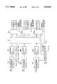
- FIG. 1 is a block diagram showing the overall construction according to a first embodiment of the present invention
- FIGS. 2A-2C are block diagrams showing the construction of a transmitting portion according to a second embodiment of the present invention.
- FIG. 3 is a diagram describing a substituting process of multiplexed data in the second embodiment
- FIG. 4 is a block diagram showing the construction of a receiving portion of the second embodiment
- FIG. 5 is a block diagram showing the construction of a receiving portion of according to a third embodiment of the present invention.
- FIG. 6 is a block diagram describing a synchronizing circuit
- FIGS. 7A-7F are timing charts showing the operation of the synchronizing circuit
- FIGS. 8A and 8B are block diagrams showing the construction of a transmitting portion of according to a fourth embodiment of the present invention.
- FIGS. 9A and 9B are schematic diagrams describing a multiplexing process and an encoding process of the fourth embodiment
- FIG. 10 is a block diagram showing the construction of a receiving portion of the fourth embodiment.
- FIG. 11 is a block diagram showing the construction of a receiving portion according to a fifth embodiment of the present invention.
- FIG. 12 is a block diagram describing a parallel-serial transforming circuit of a transmitting portion
- FIGS. 13A-13E are timing charts showing the operation of the parallel-serial transforming circuit of the transmitting portion
- FIG. 14 is a block diagram describing a serial-parallel transforming circuit of a receiving portion according to a sixth embodiment of the present invention.
- FIG. 15A-15D are timing charts showing the operation of the serial-parallel transforming circuit of a receiving portion
- FIG. 16 shows the configuration of the sending equipment according to a seventh embodiment of the present invention.
- FIG. 17 shows the configuration of the receiving equipment of the seventh embodiment
- FIG. 18 shows another configuration sample of the receiving equipment of the seventh embodiment
- FIG. 19 shows the configuration of the sending equipment according to the eighth embodiment of the present invention.
- FIG. 20 shows the configuration of the receiving equipment of the eighth embodiment.
- FIG. 21 shows the configuration of the multiplying circuit using a PLL loop.
- FIG. 1 is a block diagram showing the overall construction of a first embodiment.
- reference numerals 1 1 to 1 N are parallel-serial transforming circuits (P/S).
- Reference numeral 2 is a frame information generating circuit.
- Reference numeral 3 is a clock frequency multiplying circuit.
- Reference numeral 4 is a data substituting circuit for substituting multiplexed data.
- Reference numerals 5 1 to 5 N are electro-opto transforming circuits (E/O), These parts construct a transmitting portion.
- Reference numerals 7 1 to 7 N are optical-electric transforming circuits (O/E).
- Reference numerals 8 1 to 8 N are synchronizing circuits.
- Reference numeral 9 is a clock frequency dividing circuit.
- Reference numeral 10 is a data substituting circuit for substituting multiplexed data.
- Reference numerals 11 1 to 11 N are serial-parallel transforming circuits (S/P). These parts construct a receiving portion.
- the plurality of parallel-serial transforming circuits 1 1 to 1 N transform parallel data 1 to p, p+1 to 2p, . . . , and p(q-1) to pq-1, where a plurality of channels are separated into a plurality of groups, into multiplexed data of serial signals.
- the frame generating circuit 2 generates frame information which represents the position of a multiplexed frame.
- the clock frequency multiplying circuit 3 multiplies the frequency of the input clock by a predetermined number.
- the multiplexing clock where the frequency of the input clock is multiplied by the predetermined number is generated.
- the data substituting circuit 4 mutually substitutes the transformed results of the plurality of parallel-serial transforming circuits 11 to 1N from time to time and generates encoded data of the plurality of lines, each of which contains frame information as additional data.
- the respective encoded data are output to the plurality of electro-opto transforming circuits 5 1 to 5 N .
- the respective outputs of the electro-opto transforming circuits 5 1 to 5 N are sent to the optical fiber lines 6 1 to 6 N .
- the input signals composed of parallel data of a plurality of channels and the additional data necessary for code transformation are separated into a plurality of groups.
- the parallel data is transformed into serial data by the multiplexing clock.
- the transformed results of the plurality of circuits are mutually substituted from time to time.
- encoded data of the plurality of circuits, each of which contains the additional data are generated. Consequently, parallel data of the plurality of circuits are transmitted as encoded data.
- the plurality of opto-electro transforming circuits 7 1 to 7 N transform respective inputs of the optical fiber lines 6 1 to 6 N into electric signals.
- the plurality of synchronizing circuits 8 1 to 8 N synchronize the received multiplexed data in accordance with the frame information being inserted.
- the encoded data of the plurality of circuits are synchronized by the additional data.
- the data substituting circuit 10 substitutes the encoded data of the plurality of lines in the reverse order of the transmitting portion. In addition, the substituting circuit 10 removes the frame information as the additional information and arranges the resultant data of the plurality of circuit from time to time. Thus, the arrangement of the original multiplexed data is restored.
- the encoded data of the plurality of lines are substituted in the reverse order of the transmitting portion.
- the additional data is removed from the substituted data.
- the resultant data f the plurality of lines are arranged from time to time. From he encoded data of the plurality of lines, parallel data of the plurality of channels are decoded.
- the frequency dividing circuit 9 divides the frequency of the multiplexing clock obtained from the opto-electro transforming circuit 7 N by a predetermined value and generates the original clock.
- the frequency of transmission line clock is divided by the predetermined number and thereby the original clock is generated.
- the plurality of serial-parallel transforming circuits 111 to 11N transform respective multiplexed data from the data substituting circuit 10 into parallel data of 1 to p, p+1 to 2p, . . . , and p(q-1) to pq-1 by using the multiplexing clock and the clock from the frequency dividing circuit 9.
- data is not encoded whenever multiplexed in all the transmission lines, but in one of them.
- these data are transmitted in parallel, they are separated into multiplexed data and encoded data over the optical transmission lines.
- encoded data is always present once in a particular time period of each data transmission of each optical fiber line.
- the rise ratio of the transmission speed can be decreased to a smaller value.
- p: 1 parallel-serial transforming circuits shown in FIG. 1 are used, data with the parallel degree of pq-1 can be transmitted in parallel. In this case, the clock speed of the transmission line is suppressed to p times the speed of the original clock.
- FIG. 2A shows the construction of a transmitting portion of the second embodiment of the present invention.
- Reference numerals 31a to 31c are parallel-serial transforming circuits.
- Reference numeral 32 is a 1/2 frequency dividing circuit.
- Reference numeral 33 is a clock frequency multiplying circuit.
- Reference numeral 34 is a data substituting circuit for the transmitting portion.
- Reference numerals 35a to 35c are electro-opto transforming circuits.
- Reference numerals 36a to 36c are optical fiber lines.
- FIG. 3 describes a substituting technique of multiplexed data of the second embodiment shown in FIG. 2A.
- the data input parallel degree is 11.
- the parallel-serial transforming circuit 31a transforms parallel data of data 1 to data 4 into serial data by using a clock and a 4 times frequency clock received from the frequency multiplying circuit 33.
- data of 1234-1, 1234-2, and 1234-3 are generated as shown in FIG. 2C. These data are substituted in the order of 1), 3), and 2) by the data substituting circuit 34.
- the resultant data are sent to the electro-opto transforming circuits 35a, 35c, and 35b.
- the parallel-serial transforming circuit 31b transforms parallel data of data 5 to data 8 into serial data. As shown in the FIG. 2C, data of 5678-1, 5678-2, and 5678-3 are generated.
- the resultant data are sent to the electro-opto transforming circuits 35b, 35a, and 35c.
- the parallel-serial transforming circuit 31c transforms parallel data of data 9 to data 10 and a frame signal into serial data.
- data of 91011F-1, 91011F-2, and 91011F-3 are generated.
- the resultant data are sent to the electro-opto transforming circuits 35c, 35b, and 35a.
- the electro-opto transforming circuits 35a, 35b, and 35c transform these electric signals into optical signals and send the resultant signals to the optical fiber lines 36a, 36b, and 36c, respectively.
- FIG. 2B shows the configuration of the data substituting circuit 34 for substituting multiplexed data as described above.
- the substituting circuit 34 comprises a 3 ⁇ 3 matrix switch 34-1 and a substituting control unit 34-2.
- the above described substituting control unit 34-2 comprises a 311 dividing circuit shown in FIG. 2B(a).
- the 3/1 dividing circuit comprises three DFFs 1, 2, and 3, and an OR gate.
- Each of the DFFs 1, 2, and 3 divides a clock (for example, 100 MHz) by 3, each division being performed by 1 clock delay, and outputs a signal comprising three phases shown in FIG. 2B(b). Then, three types of timing signals are sequentially switched and outputted to the 3 ⁇ 3 matrix switch 34-1 by the substituting control unit 34-2.
- Multiplexed serial data are inputted from the parallel-serial converting circuits 31a, 3lb, and 31c to the 3 ⁇ 3 matrix switch 34-1.
- the 3 ⁇ 3 matrix switch 34-1 outputs the data according to the three types of timing signals sequentially switched based on the above described clock and inputted.
- the data 1234-1 inputted from the parallel-serial converting circuit 31a are outputted to system 1
- the data 5678-1 inputted from the parallel-serial converting circuit 3lb are outputted to system 2
- the data 91011F-1 inputted from the parallel-serial converting circuit 31c are outputted to system 3.
- the data 1234-2 inputted from the parallel-serial converting circuit 31a are outputted to system 3
- the data 5678-2 inputted from the parallel-serial converting circuit 3lb are outputted to system 1
- the data 91011F-2 inputted from the parallel-serial converting circuit 31c are outputted to system 2.
- the data 1234-3 inputted from the parallel-serial converting circuit 31a are outputted to system 2
- the data 5678-3 inputted from the parallel-serial converting circuit 31b are outputted to system 3
- the data 91011F-3 inputted from the parallel-serial converting circuit 31c are outputted to system 1.
- FIG. 4 shows the construction of a receiving portion of the second embodiment.
- Reference numerals 37a to 37c are opto-electro transforming circuits.
- Reference numerals 38a to 38c are synchronizing circuits.
- Reference numeral 39 is a high speed clock (multiplexing clock) frequency dividing circuit.
- Reference numeral 40 is a data substituting circuit for the receiving portion.
- Reference numerals 41a to 41c are parallel-serial transforming circuits.
- the opto-electro transforming circuits 37a to 37c transform optical signals received from the optical fiber lines 36a to 36c into electric signals.
- the synchronizing circuits 38a to 38c synchronize these signals (multiplexed data) by using frame information (F) contained therein and output the resultant signals to the data substituting circuit 40.
- the data substituting circuit 30 substitutes the received data in the reverse order of the data substituting circuit shown in FIG. 3. In addition, the data substituting circuit 30 removes the frame information and reproduces parallel data of data 1 to data 4, data 5 to data 8, and data 9 to data 11.
- FIG. 5 shows an example of construction where data of one transmission line is synchronized and then data of other transmission lines are synchronized therewith. The operation of this construction will be described as a third embodiment.
- FIG. 5 for simplicity, the same portions as FIG. 4 use the same reference numerals thereof.
- the synchronizing circuit 38b of the second transmission line and the third synchronizing circuit 38c of the third transmission line synchronize the data of the respective circuits in accordance with the synchronizing information detected by the synchronizing circuit 38a of the first transmission line. Except for this point, the operation of the third embodiment is the same as that of the second embodiment shown in FIG. 4.
- the constructions of the synchronizing circuits 38b and 38c can be simplified. As a result, the overall circuit scale of the apparatus can be reduced.
- FIG. 6 shows examples of multiple units as the basic construction of the synchronizing circuit.
- reference numerals 6 1 to 6 N are transmission lines.
- Reference numeral 21 (8 1 ) is a first synchronizing circuit.
- Reference numerals 22-1 to 22-i (8 2 to 8 N ) are second synchronizing circuits.
- the transmission line 61 is used as a reference line.
- a delay circuit 15 which provides a delay larger than the skew which takes place over the transmission line 6 1 is disposed thereon.
- the first synchronizing circuit 21 comprises a comparator 21a, a frame generator 2lb, a phase shifter 21c, and a protecting circuit 21d.
- each of the second synchronizing circuits 22-1 to 22-i comprises a delay circuit 22a, a control circuit 22b, a comparator 22c, and a protecting circuit 22d.
- FIG. 6 shows only the second synchronizing circuit 22-1 disposed over the transmission line 6 2 .
- Each construction of the second synchronizing circuits 22-3 to 22-N disposed over the transmission lines 6 3 to 6 N is the same as that of the second synchronizing circuit 22-2 disposed over the transmission line 6 2 .
- the mB1F code consists of data of m bits and frame information F (additional code) of 1 bit.
- FIG. 7A shows reference data which has been delayed by the delay circuit 15.
- FIG. 7B shows data transmitted over the transmission line 6 2 .
- FIG. 7C shows data transmitted over the transmission line 6 N . All these data have different delays over respective transmission lines due to skew affects of different length of optical fiber lines and different refraction indexes thereof.
- FIG. 7D shows a frame synchronous signal which is output from the frame generator 2lb of the first synchronizing circuit 21. This frame synchronous signal is sent to the second synchronizing circuits 22-1 to 22-i.
- the comparator 22c compares the frame synchronizing signal with the data received through the transmission lines 6 2 to 6 N . Until the frame F of the data of the transmission lines 6 2 to 6 N accords with the frame synchronizing signal (see FIGS. 7D, E, and F), the control circuit 22b continues to activate the delay circuit 22a. Thus, the data received through the transmission line 6 2 (FIG. 13B) is delayed by 7 bits and thereby data as shown in FIG. 7E takes place. On the other hand, the data received through the transmission line 6 N (FIG. 7C) is delayed by 5 bits and thereby data as shown in FIG. 7F takes place.
- the skew effects can be removed.
- the phases of frames of all data can be matched and data of all transmission lines can be synchronized.
- the positions of frame synchronizing signals deviate by a predetermined number of bits in the data substituting order in a predetermined time period from line to line.
- the controlling circuit 22b compensates these deviations and calculates the number of bits necessary for the delay.
- FIG. 8A shows the construction of a transmitting portion of the fourth embodiment.
- this construction when data is multiplexed, it is substituted.
- Reference numerals 45a to 45i are selecting circuits.
- Reference numeral 46 is a controlling circuit for controlling the selection of an input of each selecting circuit.
- the selecting circuits 45a to 45i separate data 1 to data 11 into a plurality of groups in different times 1, 2, and 3 by the controlling circuit 46 and substitute one data of a group which varies from time to time with additional data for code transformation.
- the low order data following the position of the additional data are successively shifted down.
- the resultant data is generated for each group.
- the plurality of parallel-serial transforming circuits 31a to 31c successively read data of the same group and transfer the resultant data as encoded data of the plurality of transmission lines to the fiber lines 1 to 3 in parallel. Since the position in which the additional bit (frame information F) is inserted deviates from line to line as shown in FIGS. 9A and 9B, the encoded data shown in FIG. 3 can be obtained.
- FIG. 8B shows the configuration of the above described selecting circuit 45a.
- Signal F is inputted to one receiving terminal of the AND circuit 45a-1 in the selecting circuit 45a.
- a selection signal is inputted from the controlling circuit 46 shown in FIG. 8A.
- Signal 4 is inputted to one receiving terminal of another AND circuit 45a-2 in the selecting circuit 45a, and to another receiving terminal, an inverted selection signal is inputted from the controlling circuit 46 shown in FIG. 8A.
- the 0R circuit 45a-3 receives the outputs from the above described AND circuits 45a-1 and 45a-2.
- the configuration of the selecting circuit 45a is the same as that in the selecting circuits 45b-45i. Therefore, when signal F is selected by the selecting circuit 45a, signals 4-11 are sequentially processed in the following selecting circuits (FIG. 8A).
- the controlling circuit 46 has two signal lines (not shown in FIG. 8A), one of which is connected to the selecting circuits 45a-45e, and the other of which is connected to the selecting circuits 45e-45i. When the selection signal in one signal line indicates "L" level and signal 4 is selected by the selecting circuit 45a, signal F is selected by the selecting circuit 45e if the selection signal of the other signal line indicates "H" level, and signal F is selected by the selecting circuit 45i if it indicates "L" level.
- FIG. 10 shows the construction of a receiving portion in accordance with the transmitting portion shown in FIG. 8A.
- the same portions as FIG. 4 use the same reference numerals thereof.
- Reference numerals 47a to 47h are selecting circuits.
- Reference numeral 48 is a controlling circuit for controlling the selection of an input of each selecting circuit 47a-47h.
- the opto-electro transforming circuits 37a to 37c transform optical signals from the optical fiber lines 36a to 36c into electric signals.
- the synchronizing circuits 38a to 38c synchronize these signals (multiplexed data) by using frame information (F) contained therein and output the resultant signals to the plurality of serial-parallel transforming circuits 41a to 41c.
- the serial-parallel transforming circuits 41a to 41c successively transform the multiplexed data received from the fiber lines into parallel data.
- the selecting circuits 47a to 47h perform the reverse processes of the multiplexing process and the encoding process shown in FIG. 9 under the control of the controlling circuit 48. In other words, the selecting circuits 47a to 47h remove the additional data from the parallel data of the same group and shift up the low order data.
- parallel data of data 1 to data 4, data 5 to data 8, and data 9 to data 11 are generated.
- the clock signal is transmitted over an optical fiber line 36d as shown in FIG. 11.
- the clock signal can be used in the decoding portion of the receiving portion. This construction can be applied to the second embodiment shown in FIG. 4 and the third embodiment shown in FIG. 5.
- the clock extracting circuit can be omitted in the receiving portion, the circuit scale of the apparatus can be reduced.
- the synchronizing process for signals of each transmission line can be omitted in the receiving portion.
- the circuit scale of the apparatus can be further reduced.
- the time necessary for the synchronizing process is not necessary, the process speed can be further improved.
- a parallel-serial transforming circuit of the transmitting portion is shown in FIG. 12.
- the operational time chart of the parallel-serial transforming circuit 1 is shown in FIGS. 13A-E.
- FIG. 12 shows the parallel-serial transforming circuit 1, the frame information generating portion 2, the clock frequency multiplying circuit 3, and the data substituting circuit 4.
- the frequency multiplying circuit 3 supplies a multiplexing clock C where the frequency of the clock C is multiplied by (m+1) as shown in FIG. 13D to the parallel-serial transforming circuit 1 as a transmission line clock shown in FIG. 13D.
- the parallel-serial transforming circuit 1 outputs serial data where data 1, data 2, . . . , data m, and additional code F are multiplexed as shown in FIG. 13E.
- the multiplexing process and the encoding process can be performed at the same time.
- FIG. 14 shows its configuration
- FIG. 15 shows the operational time chart thereof.
- FIG. 14 shows the construction of the optical fiber line 6, the opto-electro transforming circuit 7, the synchronizing circuit 8, the frequency dividing circuit 9, and the serial-parallel transforming circuit 11.
- the opto-electro transforming circuit 7 transforms a multiplexed signal received through the optical fiber line 6 into an electric signal and outputs the resultant signal as multiplexed serial data as shown in FIG. 15A.
- the opto-electro transforming circuit 7 transforms the transmission line clock where the frequency of the original clock is multiplied by (m+1) into an electric signal and outputs the resultant signal as a multiplexing clock as shown in FIG. 15B.
- the synchronizing circuit 8 extracts the position information of additional code in the serial data, that is, the frame information F, and outputs this information to the frequency dividing circuit 9.
- the frequency dividing circuit 9 divides the frequency of the multiplexing clock by (m+1) and reproduces the original clock C corresponding to the input data 1 to input data m. With respect to the multiplexed serial data, the output phase of the reproduced clock C shown in FIG. 15C is determined with the frame information F detected by the synchronizing circuit 8.
- the serial-parallel transforming circuit 11 removes the additional code data from the serial data and outputs parallel data of data 1 to data m.
- data is encoded by inserting (adding) the frame signal.
- the data is decoded by removing the frame signal. With the original clock, the output serial signal of each transmission line is transformed into parallel data.
- the above described sixth embodiment refers to one optical fiber of a transmission line.
- the transmission line of n optical fibers (n indicates a positive integer) is described as the seventh embodiment (that is, a parallel transmission at an optical level).
- the sending equipment is configured as shown in FIG. 16. That is, the NOT circuit shown in FIGS.2A-2C is used instead of the frame generating circuit 2, and the P/S transforming circuit is provided with the electro-optical transforming circuit and the optical fibers such that they are configured as the NOT circuit 23 1 -23 n , the P/S converting circuit 24 1 -24 n , the transforming circuit 31 1 -31 n , and the optical fiber 33 1 -33 n each being provided in n units in parallel.
- the multiplying circuit 3 shown in FIG. 12 is shared in the configuration.
- the receiving equipment corresponding to the above described sending equipment is configured as shown in FIGS. 17 and 18.
- the electro-opto transforming circuits 72 1 -72 n are provided corresponding to the optical fiber 73 1 -73 n .
- the synchronizing circuits 67 1 -67 n , the dividers 68 1 -68 n , and the S/P converting circuits 69 1 -69 n are provided in the configuration. That is, in the configuration shown in FIG. 17, the receiving equipment comprising one optical fiber 73 is increased to n units and arranged in parallel. In this case, since the final data must be outputted as synchronizing with the same clock, the latch circuit 34 is provided at the output side of each of the S/P converting circuits 69 1 -69 n .
- the signs in the transmission line are processed in the above described configuration of the sending and receiving equipments in the same operation, but in n units in parallel.
- the configuration of the receiving equipment shown in FIG. 18 is different from that shown in FIG. 8A-8B in that it shares the divider 28 and the synchronizing circuit 27.
- the synchronizing circuit 27 detects the relative position of other data by locating a complementary sign in the multiplexed data, and transmits the detection result to the divider 28.
- the data from other optical fibers 33 1 -33 n are synchronized and S/P converted according to the synchronization result obtained by converting the data transmitted through the optical fiber 33 n to an electric signal by the electro opto transforming circuit 32 n and the extracted clock. Therefore, in this case, the latch circuit 34 shown in FIGS. 8A-8B is not required.
- the explanation up to the seventh embodiment describes how to realize the synchronization of data frames in the synchronous circuit provided in the receiving unit.
- a frame signal itself can be transmitted through optical fibers.
- the necessary configurations of the sending and the receiving equipments are shown in FIGS. 19 and 20 respectively.
- frame information is sent through optical fibers from a sending equipment, thereby requiring no synchronous circuits for synchronizing frames in a receiving equipment.
- the sending equipment comprises n sending units as in the seventh embodiment, that is, n NOT circuits 23 1 -23 n , n P/S converting circuits 24 1 -24 n , n electro-opto transforming circuit 31 1 -31 n , and a shared multiplying circuit 25.
- the eighth embodiment comprises an electro-opto transforming circuit 35 for converting frame information to an optical signal, and an optical fiber 36 for transmitting to the receiving equipment the frame information converted to the optical signal.
- the receiving equipment in FIG. 20 comprises n electro opto transforming circuits 32 1 -32 n , n S/P converting circuits 29 1 -29 n , and an electro-opto transforming circuit 37 for converting the frame information received from the above described sending equipment to an electric signal.
- the receiving equipment requires no synchronization restoring time taken for synchronizing frames can be reduced to zero.
- a transmission code can be an mB1C (m bit+one complementary code), an mB1F (m bit+one frame signal), or an mB1P code having a parity signal P for a signal 1-m. That is, the code can comprise m bits and an additional 1 bit to form a transmission code applied to the present invention. Besides, m bits and additional n bits (n indicates a positive integer larger than 1) instead of m bits and an additional 1 bit can be applied to the present embodiment as long as the frequency of the multiplexed clock equals the value obtained by multiplying the value of the input data clock by "m+n".
- FIG. 21 shows the configuration of the multiplying circuit.
- 41 is a phase comparing circuit
- 42 is a voltage control oscillator
- 43 is a 1/(m+1) divider.
- a transmission line code is inserted as an additional bit for every m-th bit.
Landscapes
- Engineering & Computer Science (AREA)
- Computer Networks & Wireless Communication (AREA)
- Signal Processing (AREA)
- Physics & Mathematics (AREA)
- Spectroscopy & Molecular Physics (AREA)
- Power Engineering (AREA)
- Time-Division Multiplex Systems (AREA)
- Synchronisation In Digital Transmission Systems (AREA)
- Optical Communication System (AREA)
- Computer And Data Communications (AREA)
- Communication Control (AREA)
- Dc Digital Transmission (AREA)
Applications Claiming Priority (2)
| Application Number | Priority Date | Filing Date | Title |
|---|---|---|---|
| JP23267991A JP3158213B2 (ja) | 1991-09-12 | 1991-09-12 | 並列伝送方法および装置 |
| JP3-232679 | 1991-09-12 |
Publications (1)
| Publication Number | Publication Date |
|---|---|
| US5426644A true US5426644A (en) | 1995-06-20 |
Family
ID=16943097
Family Applications (1)
| Application Number | Title | Priority Date | Filing Date |
|---|---|---|---|
| US07/944,239 Expired - Fee Related US5426644A (en) | 1991-09-12 | 1992-09-14 | Parallel code transmission method and apparatus of the same |
Country Status (5)
| Country | Link |
|---|---|
| US (1) | US5426644A (de) |
| EP (1) | EP0533091B1 (de) |
| JP (1) | JP3158213B2 (de) |
| CA (1) | CA2078040C (de) |
| DE (1) | DE69231871T2 (de) |
Cited By (18)
| Publication number | Priority date | Publication date | Assignee | Title |
|---|---|---|---|---|
| US5694612A (en) * | 1994-06-17 | 1997-12-02 | International Business Machines Corporation | Self-timed interface for a network of computer processors interconnected in parallel |
| US5818846A (en) * | 1995-01-26 | 1998-10-06 | Hitachi Denshi Kabushiki Kaisha | Digital signal transmission system |
| US5978419A (en) * | 1997-06-24 | 1999-11-02 | Sun Microsystems, Inc. | Transmitter and receiver circuits for high-speed parallel digital data transmission link |
| US20010033568A1 (en) * | 2000-03-15 | 2001-10-25 | Lucent And Agere | Data communication link |
| US6353622B1 (en) * | 1995-09-29 | 2002-03-05 | Siemens Aktiengesellschaft | Process for maintaining the microsynchronous operation of double information-processing units |
| US6370200B1 (en) * | 1997-08-04 | 2002-04-09 | Matsushita Electric Industrial Co., Ltd. | Delay adjusting device and method for plural transmission lines |
| US20020181053A1 (en) * | 2001-05-30 | 2002-12-05 | Nec Corporation | Optical communication system including replaceable electro-optic and opto-electric converters |
| US20020186439A1 (en) * | 2001-06-06 | 2002-12-12 | Buabbud George H. | Wavelength division multiplexed (WDM) ring passive optical network (PON) with route protection for replacement of splitter based passive optical networks |
| US6583737B2 (en) | 1999-09-03 | 2003-06-24 | Infineon Technologies Ag | Device and method for compensating for propagation delay |
| US6628214B1 (en) * | 1998-09-01 | 2003-09-30 | Seiko Epson Corporation | Deserializer, semiconductor device, electronic device, and data transmission system |
| US20040114585A1 (en) * | 2002-12-17 | 2004-06-17 | Kraemer Finn Leif | Clock provisioning techniques |
| US20050063707A1 (en) * | 2003-08-07 | 2005-03-24 | Nobuyuki Imai | Method for transmitting digital image signal, digital image transmitting device, digital image sending device and digital image receiver |
| US6889272B1 (en) * | 2000-11-03 | 2005-05-03 | Applied Micro Circuits Corporation | Parallel data bus with bit position encoded on the clock wire |
| EP1278320A3 (de) * | 2001-07-19 | 2006-03-15 | Broadcom Corporation | Schaltung zur Serialisierung von synchronen Daten |
| US7573916B1 (en) * | 1999-06-25 | 2009-08-11 | Cisco Technology, Inc. | Multi-function high-speed network interface |
| US20110299316A1 (en) * | 2002-06-24 | 2011-12-08 | Choi Jung-Hwan | Memory module, method and memory system having the memory module |
| US20130177324A1 (en) * | 2012-01-06 | 2013-07-11 | Fuji Xerox Co., Ltd. | Sending/receiving system, sending/receiving method, and non-transitory computer-readable medium |
| US20130236168A1 (en) * | 2012-03-06 | 2013-09-12 | Fujitsu Limited | Optical transmission apparatus and optical transmission method |
Families Citing this family (12)
| Publication number | Priority date | Publication date | Assignee | Title |
|---|---|---|---|---|
| JP3110104B2 (ja) * | 1991-10-07 | 2000-11-20 | 富士通株式会社 | 交換機 |
| GB2280338B (en) * | 1993-07-16 | 1997-09-24 | Motion Media Techn Ltd | Multiple bit stream multiplexor/demultiplexor for communication channels |
| JP2715900B2 (ja) * | 1994-03-30 | 1998-02-18 | 日本電気株式会社 | 並列データ伝送装置 |
| JPH08293834A (ja) * | 1995-04-24 | 1996-11-05 | Fujitsu Ltd | 光パラレル伝送方式および光伝送装置 |
| JP3357581B2 (ja) | 1997-08-04 | 2002-12-16 | 日本電信電話株式会社 | 信号多重化装置 |
| FR2782430B1 (fr) * | 1998-08-13 | 2004-05-28 | Bull Sa | Procede et interface d'interconnection mettant en oeuvre des liaisons serie haut-debit |
| EP0996262A1 (de) | 1998-10-22 | 2000-04-26 | Texas Instruments France | Kommunikationssystem mit mehreren synchronisierten Datenverbindungen |
| US6832277B2 (en) * | 2001-08-02 | 2004-12-14 | Sun Microsystems, Inc. | Method and apparatus for transmitting data that utilizes delay elements to reduce capacitive coupling |
| US7035368B2 (en) | 2002-03-18 | 2006-04-25 | Texas Instruments Incorporated | High speed parallel link receiver |
| RU2234809C2 (ru) * | 2002-06-06 | 2004-08-20 | Зангиев Владимир Юрьевич | Способ организации связи и обмена информацией |
| JP6243210B2 (ja) * | 2013-12-09 | 2017-12-06 | Necプラットフォームズ株式会社 | シリアルデータ送信装置、シリアルデータ受信装置、シリアルデータ送信方法、及び、シリアルデータ送信プログラム |
| FR3094593B1 (fr) * | 2019-03-29 | 2021-02-19 | Teledyne E2V Semiconductors Sas | Procédé de synchronisation de données numériques envoyées en série |
Citations (12)
| Publication number | Priority date | Publication date | Assignee | Title |
|---|---|---|---|---|
| US3708783A (en) * | 1971-06-18 | 1973-01-02 | Ampex | Interchannel time displacement correction method and apparatus |
| JPS5795737A (en) * | 1980-12-05 | 1982-06-14 | Fujitsu Ltd | Multiplex data transmission device |
| JPS5836052A (ja) * | 1981-08-26 | 1983-03-02 | Fujitsu Ltd | 並列デ−タ伝送方式 |
| US4520480A (en) * | 1982-05-18 | 1985-05-28 | Nec Corporation | Digital transmission system |
| EP0225025A2 (de) * | 1985-11-23 | 1987-06-10 | International Computers Limited | Datenübertragungssystem |
| GB2191662A (en) * | 1986-05-19 | 1987-12-16 | Hitachi Ltd | Parallel transmission system |
| US4727541A (en) * | 1984-12-06 | 1988-02-23 | Fujitsu Limited | Hierarchical data transmission system |
| EP0436293A2 (de) * | 1990-01-02 | 1991-07-10 | AT&T Corp. | Inverse Multiplexer- und Demultiplexerverfahren |
| US5136587A (en) * | 1989-01-09 | 1992-08-04 | Fujitsu Limited | Digital signal multiplexing apparatus and demultiplexing apparatus |
| US5150364A (en) * | 1990-08-24 | 1992-09-22 | Hewlett-Packard Company | Interleaved time-division demultiplexor |
| US5212687A (en) * | 1990-12-14 | 1993-05-18 | U. S. Philips Corporation | Arrangement for transmitting over a time-division multiplex line different channels having various bit rates |
| US5216671A (en) * | 1990-12-13 | 1993-06-01 | Rca Licensing Corporation | High speed bit serial systems |
-
1991
- 1991-09-12 JP JP23267991A patent/JP3158213B2/ja not_active Expired - Fee Related
-
1992
- 1992-09-11 CA CA002078040A patent/CA2078040C/en not_active Expired - Fee Related
- 1992-09-14 EP EP92115692A patent/EP0533091B1/de not_active Expired - Lifetime
- 1992-09-14 DE DE69231871T patent/DE69231871T2/de not_active Expired - Fee Related
- 1992-09-14 US US07/944,239 patent/US5426644A/en not_active Expired - Fee Related
Patent Citations (12)
| Publication number | Priority date | Publication date | Assignee | Title |
|---|---|---|---|---|
| US3708783A (en) * | 1971-06-18 | 1973-01-02 | Ampex | Interchannel time displacement correction method and apparatus |
| JPS5795737A (en) * | 1980-12-05 | 1982-06-14 | Fujitsu Ltd | Multiplex data transmission device |
| JPS5836052A (ja) * | 1981-08-26 | 1983-03-02 | Fujitsu Ltd | 並列デ−タ伝送方式 |
| US4520480A (en) * | 1982-05-18 | 1985-05-28 | Nec Corporation | Digital transmission system |
| US4727541A (en) * | 1984-12-06 | 1988-02-23 | Fujitsu Limited | Hierarchical data transmission system |
| EP0225025A2 (de) * | 1985-11-23 | 1987-06-10 | International Computers Limited | Datenübertragungssystem |
| GB2191662A (en) * | 1986-05-19 | 1987-12-16 | Hitachi Ltd | Parallel transmission system |
| US5136587A (en) * | 1989-01-09 | 1992-08-04 | Fujitsu Limited | Digital signal multiplexing apparatus and demultiplexing apparatus |
| EP0436293A2 (de) * | 1990-01-02 | 1991-07-10 | AT&T Corp. | Inverse Multiplexer- und Demultiplexerverfahren |
| US5150364A (en) * | 1990-08-24 | 1992-09-22 | Hewlett-Packard Company | Interleaved time-division demultiplexor |
| US5216671A (en) * | 1990-12-13 | 1993-06-01 | Rca Licensing Corporation | High speed bit serial systems |
| US5212687A (en) * | 1990-12-14 | 1993-05-18 | U. S. Philips Corporation | Arrangement for transmitting over a time-division multiplex line different channels having various bit rates |
Non-Patent Citations (4)
| Title |
|---|
| Patent Abstracts of Japan, vol. 6, No. 182 (E 131) & JP A 57 095 737 (Fujitsu Ltd.) *abstract*. * |
| Patent Abstracts of Japan, vol. 6, No. 182 (E-131) & JP-A-57 095 737 (Fujitsu Ltd.) *abstract*. |
| Patent Abstracts of Japan, vol. 7, No. 119 (E 177)(1264) & JP A 58 36 052 (Fujitsu K.K.) *abstract*. * |
| Patent Abstracts of Japan, vol. 7, No. 119 (E-177)(1264) & JP-A-58 36 052 (Fujitsu K.K.) *abstract*. |
Cited By (29)
| Publication number | Priority date | Publication date | Assignee | Title |
|---|---|---|---|---|
| US5694612A (en) * | 1994-06-17 | 1997-12-02 | International Business Machines Corporation | Self-timed interface for a network of computer processors interconnected in parallel |
| US5818846A (en) * | 1995-01-26 | 1998-10-06 | Hitachi Denshi Kabushiki Kaisha | Digital signal transmission system |
| US6353622B1 (en) * | 1995-09-29 | 2002-03-05 | Siemens Aktiengesellschaft | Process for maintaining the microsynchronous operation of double information-processing units |
| US5978419A (en) * | 1997-06-24 | 1999-11-02 | Sun Microsystems, Inc. | Transmitter and receiver circuits for high-speed parallel digital data transmission link |
| US6370200B1 (en) * | 1997-08-04 | 2002-04-09 | Matsushita Electric Industrial Co., Ltd. | Delay adjusting device and method for plural transmission lines |
| US6628214B1 (en) * | 1998-09-01 | 2003-09-30 | Seiko Epson Corporation | Deserializer, semiconductor device, electronic device, and data transmission system |
| US7573916B1 (en) * | 1999-06-25 | 2009-08-11 | Cisco Technology, Inc. | Multi-function high-speed network interface |
| US6583737B2 (en) | 1999-09-03 | 2003-06-24 | Infineon Technologies Ag | Device and method for compensating for propagation delay |
| US20010033568A1 (en) * | 2000-03-15 | 2001-10-25 | Lucent And Agere | Data communication link |
| US20060187968A1 (en) * | 2000-03-15 | 2006-08-24 | Agere Systems Inc. | Method for data communication |
| US7031347B2 (en) | 2000-03-15 | 2006-04-18 | Agere Systems Inc. | Data communication link |
| US6889272B1 (en) * | 2000-11-03 | 2005-05-03 | Applied Micro Circuits Corporation | Parallel data bus with bit position encoded on the clock wire |
| US20020181053A1 (en) * | 2001-05-30 | 2002-12-05 | Nec Corporation | Optical communication system including replaceable electro-optic and opto-electric converters |
| US7302190B2 (en) * | 2001-05-30 | 2007-11-27 | Nec Corporation | Optical communication system including replaceable electro-optic and opto-electric converters |
| US20050163147A1 (en) * | 2001-06-06 | 2005-07-28 | Buabbud George H. | Wavelength division multiplexed (WDM) ring passive optical network (PON) with route protection for replacement of splitter based passive optical networks |
| US20020186439A1 (en) * | 2001-06-06 | 2002-12-12 | Buabbud George H. | Wavelength division multiplexed (WDM) ring passive optical network (PON) with route protection for replacement of splitter based passive optical networks |
| US6898206B2 (en) * | 2001-06-06 | 2005-05-24 | Advanced Fibre Access Corporation | Wavelength division multiplexed (WDM) ring passive optical network (PON) with route protection for replacement of splitter based passive optical networks |
| US7212541B2 (en) | 2001-06-06 | 2007-05-01 | Bedford Tellabs, Inc. | Wavelength division multiplexed (WDM) ring passive optical network (PON) with route protection for replacement of splitter based passive optical networks |
| US20070201873A1 (en) * | 2001-06-06 | 2007-08-30 | Tellabs Bedford, Inc. | Wavelength Division Multiplexed (WDM) Ring Passive Optical Network (PON) with Route Protection for Replacement of Splitter Based Passive Optical Networks |
| EP1278320A3 (de) * | 2001-07-19 | 2006-03-15 | Broadcom Corporation | Schaltung zur Serialisierung von synchronen Daten |
| US20110299316A1 (en) * | 2002-06-24 | 2011-12-08 | Choi Jung-Hwan | Memory module, method and memory system having the memory module |
| US20040114585A1 (en) * | 2002-12-17 | 2004-06-17 | Kraemer Finn Leif | Clock provisioning techniques |
| US7440702B2 (en) * | 2003-08-07 | 2008-10-21 | Seiko Epson Corporation | Method for transmitting digital image signal, digital image transmitting device, digital image sending device and digital image receiver |
| US20050063707A1 (en) * | 2003-08-07 | 2005-03-24 | Nobuyuki Imai | Method for transmitting digital image signal, digital image transmitting device, digital image sending device and digital image receiver |
| US20130177324A1 (en) * | 2012-01-06 | 2013-07-11 | Fuji Xerox Co., Ltd. | Sending/receiving system, sending/receiving method, and non-transitory computer-readable medium |
| JP2013141183A (ja) * | 2012-01-06 | 2013-07-18 | Fuji Xerox Co Ltd | 送受信システム及びプログラム |
| US8897650B2 (en) * | 2012-01-06 | 2014-11-25 | Fuji Xerox Co., Ltd. | Sending/receiving system, sending/receiving method, and non-transitory computer-readable medium |
| US20130236168A1 (en) * | 2012-03-06 | 2013-09-12 | Fujitsu Limited | Optical transmission apparatus and optical transmission method |
| US9071348B2 (en) * | 2012-03-06 | 2015-06-30 | Fujitsu Limited | Optical transmission apparatus and optical transmission method |
Also Published As
| Publication number | Publication date |
|---|---|
| DE69231871T2 (de) | 2001-11-15 |
| CA2078040C (en) | 1999-03-16 |
| DE69231871D1 (de) | 2001-07-19 |
| EP0533091A3 (en) | 1993-09-08 |
| EP0533091B1 (de) | 2001-06-13 |
| CA2078040A1 (en) | 1993-03-13 |
| JP3158213B2 (ja) | 2001-04-23 |
| JPH05183526A (ja) | 1993-07-23 |
| EP0533091A2 (de) | 1993-03-24 |
Similar Documents
| Publication | Publication Date | Title |
|---|---|---|
| US5426644A (en) | Parallel code transmission method and apparatus of the same | |
| EP0206408B1 (de) | Digitales Übertragungssystem höherer Ordnung welches einen Multiplexer und einen Demultiplexer enthält | |
| EP0535768B1 (de) | Übertragungssystem mit beliebiger Parallelrahmensynchronisierungsanordnung | |
| JPH0648870B2 (ja) | 光通信網および光通信網の同期方法 | |
| EP1665809B1 (de) | System und verfahren zur bildung einer bidirektionalen multimediaverbindung | |
| US6667994B1 (en) | Multiplexing digital communication system | |
| JPH0290827A (ja) | 分岐挿入型多重変換装置 | |
| US4829518A (en) | Multiplexing apparatus having BSI-code processing and bit interleave functions | |
| US20020097752A1 (en) | Communications system and associated deskewing and word framing methods | |
| US5430733A (en) | Digital transmission system for multiplexing and demultiplexing signals | |
| AU667602B2 (en) | Multiplexing arrangement | |
| EP0206409B1 (de) | Digitales Übertragungssystem höherer Ordnung welches einen Multiplexer und einen Demultiplexer enthält | |
| US6686856B1 (en) | Clocking domain conversion system and method | |
| EP0622004A1 (de) | Optische verarbeitung in einem atm netz | |
| US7262645B2 (en) | System and method for adjusting the phase of a frequency-locked clock | |
| US4498167A (en) | TDM Communication system | |
| GB2294850A (en) | Digital transmission system clock extraction circuit | |
| JPH0556025A (ja) | 伝送路符号処理方式 | |
| JPH09275380A (ja) | ディジタル映像信号の時分割多重方法及び装置 | |
| JPH0282830A (ja) | データ変換中継方式 | |
| JPS60158746A (ja) | 同期装置 | |
| JPH06188867A (ja) | ディジタル信号通信方式 | |
| Regnier | Synchronous Digital Fiber Optic Networks for Multi-Channel Video Transmission | |
| JPS62151045A (ja) | 多重変換装置の同期信号伝送方式 | |
| JPH02302137A (ja) | 分岐中継伝送方法 |
Legal Events
| Date | Code | Title | Description |
|---|---|---|---|
| AS | Assignment |
Owner name: FUJITSU LIMITED, JAPAN Free format text: ASSIGNMENT OF ASSIGNORS INTEREST.;ASSIGNOR:FUJIMOTO, NOBUHIRO;REEL/FRAME:006263/0273 Effective date: 19920902 |
|
| CC | Certificate of correction | ||
| FEPP | Fee payment procedure |
Free format text: PAYOR NUMBER ASSIGNED (ORIGINAL EVENT CODE: ASPN); ENTITY STATUS OF PATENT OWNER: LARGE ENTITY |
|
| FPAY | Fee payment |
Year of fee payment: 4 |
|
| FPAY | Fee payment |
Year of fee payment: 8 |
|
| REMI | Maintenance fee reminder mailed | ||
| LAPS | Lapse for failure to pay maintenance fees | ||
| STCH | Information on status: patent discontinuation |
Free format text: PATENT EXPIRED DUE TO NONPAYMENT OF MAINTENANCE FEES UNDER 37 CFR 1.362 |
|
| FP | Lapsed due to failure to pay maintenance fee |
Effective date: 20070620 |