US5444412A - Programming voltage regulation circuit for programmable memories - Google Patents
Programming voltage regulation circuit for programmable memories Download PDFInfo
- Publication number
- US5444412A US5444412A US08/196,160 US19616094A US5444412A US 5444412 A US5444412 A US 5444412A US 19616094 A US19616094 A US 19616094A US 5444412 A US5444412 A US 5444412A
- Authority
- US
- United States
- Prior art keywords
- voltage
- circuit
- load pump
- voltage vpp
- regulator
- Prior art date
- Legal status (The legal status is an assumption and is not a legal conclusion. Google has not performed a legal analysis and makes no representation as to the accuracy of the status listed.)
- Expired - Fee Related
Links
Images

Classifications
-
- G—PHYSICS
- G11—INFORMATION STORAGE
- G11C—STATIC STORES
- G11C16/00—Erasable programmable read-only memories
- G11C16/02—Erasable programmable read-only memories electrically programmable
- G11C16/06—Auxiliary circuits, e.g. for writing into memory
- G11C16/30—Power supply circuits
-
- G—PHYSICS
- G05—CONTROLLING; REGULATING
- G05F—SYSTEMS FOR REGULATING ELECTRIC OR MAGNETIC VARIABLES
- G05F1/00—Automatic systems in which deviations of an electric quantity from one or more predetermined values are detected at the output of the system and fed back to a device within the system to restore the detected quantity to its predetermined value or values, i.e. retroactive systems
- G05F1/10—Regulating voltage or current
- G05F1/46—Regulating voltage or current wherein the variable actually regulated by the final control device is DC
- G05F1/462—Regulating voltage or current wherein the variable actually regulated by the final control device is DC as a function of the requirements of the load, e.g. delay, temperature, specific voltage/current characteristic
- G05F1/465—Internal voltage generators for integrated circuits, e.g. step down generators
-
- G—PHYSICS
- G05—CONTROLLING; REGULATING
- G05F—SYSTEMS FOR REGULATING ELECTRIC OR MAGNETIC VARIABLES
- G05F3/00—Non-retroactive systems for regulating electric variables by using an uncontrolled element, or an uncontrolled combination of elements, such element or such combination having self-regulating properties
- G05F3/02—Regulating voltage or current
- G05F3/08—Regulating voltage or current wherein the variable is DC
- G05F3/10—Regulating voltage or current wherein the variable is DC using uncontrolled devices with non-linear characteristics
- G05F3/16—Regulating voltage or current wherein the variable is DC using uncontrolled devices with non-linear characteristics being semiconductor devices
- G05F3/20—Regulating voltage or current wherein the variable is DC using uncontrolled devices with non-linear characteristics being semiconductor devices using diode- transistor combinations
- G05F3/24—Regulating voltage or current wherein the variable is DC using uncontrolled devices with non-linear characteristics being semiconductor devices using diode- transistor combinations wherein the transistors are of the field-effect type only
-
- G—PHYSICS
- G11—INFORMATION STORAGE
- G11C—STATIC STORES
- G11C5/00—Details of stores covered by group G11C11/00
- G11C5/14—Power supply arrangements, e.g. power down, chip selection or deselection, layout of wirings or power grids, or multiple supply levels
- G11C5/147—Voltage reference generators, voltage or current regulators; Internally lowered supply levels; Compensation for voltage drops
Definitions
- the invention relates to electrically programmable memories in integrated circuit form, generally known as "EEPROM memories” or “EPROM memories” depending on whether or not they are electrically erasable, or again “flash EPROM” memories when they are erasable in blocks.
- Vpp a voltage known as the "programming voltage" Vpp available in the integrated circuit.
- This programming voltage is substantially higher than the normal supply voltage Vcc of the circuit.
- Vcc is usually equal to 5 volts and Vpp is 15 volts or more.
- the programming voltage Vpp is given by an external supply.
- the additional terminals add to the cost of the integrated circuit, and it is preferable to avoid them.
- the number of terminals is laid down (for example: chip cards with six or eight terminals) and there is no was to add another one.
- there may even be no external supply terminals for example, a chip card without contact whose operating power is provided by an electromagnetic means).
- the programming voltage Vpp is produced right inside the integrated circuit, from the normal supply voltage Vcc.
- the circuit used is one that is conventionally called a load pump or voltage raiser that receives Vcc and sets up a voltage Vpp greater than Vcc.
- the raising circuits are standard ones: a basic raising stage uses simply switches, two capacitors and a two-phase clock to actuate the switches. In a first step, the first capacitor is charged to 5 volts, and then it is discharged into the second capacitor. Then a cycle starts again: a first step of charging the first capacitor to 5 volts and a second step of discharging it into the second capacitor (this time, the second capacitor is already partially charged); the voltage at the terminals of the second capacitor then increases at each clock stroke. Within a few two-phase clock strokes, a voltage that is thrice Vcc is reached in the second capacitor. With two stages, the voltage Vcc is multiplied by 4 within a few clock strokes etc.
- the level of output voltage from the raising circuit, available at a capacitor, is kept at a fixed value by a regulator.
- This regulator may be constituted by a line of transistors that are mounted as diodes so that each one sets up a voltage equal to its threshold voltage between its source and its drain. Depending on the technology implemented, the threshold voltage varies and the number of series-connected transistors generates the regulated voltage at output of the regulator.
- transistors having a threshold voltage on the order of one volt 16 transistors are needed to set up a regulated voltage Vpp on the order of 16 volts.
- a major drawback of existing circuits is their consumption of substantial levels of current, due to the consumption by the load pump itself as well as to that of the regulator. Now it is generally desired to lower this consumption. Furthermore, in certain cases, it is absolutely indispensable to find approaches that minimize consumption: for example, in the case of integrated circuits for "contact-free" chip cards.
- an aim of the invention is to propose a new circuit for the production of a regulated voltage, whether or not this is for a programmable memory.
- the circuit for the generation of a voltage Vpp comprises a load pump, a regulation circuit capable of stopping the load pump when the voltage Vpp gets higher than a determined threshold, means to interrupt the current consumption of the regulation circuit when the voltage Vpp gets higher than a threshold (which is preferably the same as the foregoing threshold), and a control circuit capable of detecting a small drop in the voltage Vpp below the value given by the regulation circuit, and of reactivating the load pump and the current consumption of the regulation circuit when this drop exceeds a predetermined value dV.
- the regulation circuit (or regulator) works continuously and consumes current continuously.
- the regulator is put out of operation as soon as it detects the fact that the right value of programming voltage has been reached. And it is a control circuit, consuming very little current, that examines the stability of the voltage obtained. If the voltage drops excessively, it puts both the load pump and the regulator back into operation.
- the control circuit is not equivalent to another regulator that would be similar to the first one. It may be built so as to consume very little current for its function is not to ascertain that the voltage conforms to a predetermined voltage (for example 15 volts) but to ascertain that the voltage obtained at a given moment (by means of the regulator) does not drop by more than a determined value dV (for example 0.5 volt).
- a predetermined voltage for example 15 volts
- dV for example 0.5 volt
- the regulator will be built preferably from a resistive divider formed by numerous resistors of high value (of the order of one megohm each). These resistors may be made out of P channel transistors formed in respective N type wells, separated from one another (in the case of a P type substrate), these transistors having their drain and their gain joined. The source of each transistor is preferably connected to the corresponding well.
- the regulator also has a voltage level detector (or comparator) to compare the voltage level at an intermediate point of the resistive divider with a reference.
- This detector has, for example, an input connected to one of the resistors and it may have another input receiving a reference voltage level.
- the output of this detector controls the load pump so as to be capable of interrupting its operation, and it also preferably controls a transistor for the supply of current to the resistive divider to interrupt the circulation of current in this divider.
- the assembly formed by the resistive divider and the current supply transistor is connected between the terminal of the regulator which gives the voltage Vpp and a ground.
- the control circuit preferably has a capacitor connected between a floating node and a terminal of the regulator giving the voltage Vpp.
- the floating node may be precharged to a value Vprech, and it is connected to an input of a comparator which also receives, at another input, a reference voltage equal to Vprech-dV.
- the difference in potential dV defines (directly or indirectly) a value of voltage drop that is acceptable for the voltage Vpp. It is equal, for example, to some tenths of a volt.
- the output of this comparator is connected so as to control the reactivation of the load pump and the current supply of the divider.
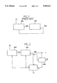
- FIG. 1 shows a block diagram of a prior art circuit
- FIG. 2 shows a block diagram of a circuit according to the invention
- FIG. 3 shows a detailed diagram of an embodiment of the invention
- FIG. 4 shows a detail of the regulator
- FIG. 5 shows a timing diagram of the signals of the circuit of FIG. 3.
- FIG. 1 recalls the prior art constitution of a circuit for the generation of a programming voltage Vpp for an EPROM or an EEPROM when the voltage has to be produced inside the integrated circuit.
- the integrated circuit is supplied with a voltage Vcc, equal for example to five volts.
- Vcc a voltage raising circuit PMP, often called a load pump because of its mode of operation.
- This load pump PMP produces a voltage VHT that is substantially higher than Vcc, for example between 15 and 20 volts.
- the voltage VHT is applied to a regulator circuit REG that gives the programming voltage Vpp from the voltage VHT.
- the voltage Vpp may be equal to the voltage VHT.
- the main function of the regulation circuit REG is to compare the voltage Vpp with a reference value, give a signal for the interruption of the load pump when Vpp exceeds a given level and start it up again if Vpp falls below this threshold (possibly with a hysteresis).
- the regulator most commonly used is a resistive divider bridge and it consumes current.
- FIG. 2 The diagram of the circuit according to the invention is shown in a general form in FIG. 2. There is still a load pump or voltage raising circuit PMP that has the same role as above and can be constituted as in the prior art.
- the load pump gives a voltage VHT, available at an output capacitor of the load pump, that is again applied to a voltage regulator circuit REG.
- This circuit gives the desired voltage Vpp (which may be voltage VHT itself). It compares the voltage Vpp with a reference value and gives a signal Sr when the voltage Vpp exceeds this reference value. This signal Sr is used to interrupt the working of the load pump.
- the regulator of FIG. 2 additionally possesses the following particular feature: it has a control input by which its current supply can be interrupted. This control input may receive a signal A that interrupts the current supply. Naturally, when the supply of the regulator is thus interrupted, it can no longer exert its function of regulation and no longer consumes any current, whether on Vcc or on Vpp.
- the signal A is prepared from the signal Sr and sent out when the voltage Vpp has reached its reference value. It is this signal that is also used to interrupt the load pump.
- the Vpp generation circuit furthermore comprises a control circuit CTRL having the following function: it receives the voltage Vpp, and it gives a signal Sc as soon as this voltage falls by more than a quantity dV below the initial value that it possesses subtantially when the working of the load pump is interrupted by the signal A.
- This control circuit therefore does not compare the voltage Vpp with an absolute reference threshold, but it starts from the initial value Vpp0 of the voltage Vpp at a given instant, and it detects the drop by a value dV to give a signal when Vpp falls below Vpp0-dV.
- Vpp0 is precisely the reference voltage reached by Vpp when the regulator sends the signal Sr to stop the load pump.
- the signal Sc sent out by the control circuit is used to restore the current supply of the regulation circuit REG and to start up the load pump PMP again.
- a logic circuit CL uses the signals Sr (coming from the regulator REG) and Sc (coming from the control circuit CTRL) to give the signal A which controls both the current supply of the regulator and the operation of the load pump.
- Sr prompts the setting up of the signal A; Sc prompts its interruption.
- the signal A appears under the control of Sr to interrupt the current supply of the regulator and interrupt the load pump as soon as the regulator has detected the fact that Vpp has reached its reference value Vpp0.
- This signal A disappears under the control of Sc to restore the current supply of the regulator and start up the load pump again as soon as the control circuit has detected the passage of Vpp to below Vpp0-dV.
- the regulator consumes current only when the voltage Vpp has to be raised by the load pump. And the necessity of raising this voltage is lessened precisely because the regulator no longer consumes any current on the conductor giving Vpp. Indeed, the fact is that the programming of memory cells by Vpp consumes very little current on Vpp. It is actually the regulator that consumes current and that makes Vpp drop in the prior art. This often makes it necessary to reactivate the load pump which, for its part, also consumes a great deal of current (on the Vcc supply).
- FIG. 3 shows a detailed diagram of a preferred mode of execution of the invention.
- the load pump PMP has not been described in detail because it may be a standard device. It has an oscillator, switches controlled in phase alternation by the oscillator, capacitors and possibly diodes. Its operation consists in switching over the capacitors alternately in parallel and then in series to make a charge flow, always in the same direction, from a first capacitor to a second capacitor. The charge gradually accumulates on the second capacitor.
- the signal A used to interrupt or start up the load pump will act quite simply by interrupting or permitting the operation of the oscillator.
- the regulation circuit REG preferably has a resistive divider bridge DR connected between the voltage Vpp (here, Vpp is directly the voltage VHT coming from the load pump) and the ground.
- a switch constituted by a transistor T1 is, however, interposed between the divider and the ground. When this switch is on, it may be considered to be a short circuit (with very low resistance as compared with that of the resistive divider). When it is off, it interrupts the passage of current in the resistive divider. The divider then no longer consumes any current and no longer works properly.
- the gate of the transistor T1 receives the signal A mentioned with reference to FIG. 2.
- the regulator REG also comprises a comparator CMP1 used as a detector of the level of the voltage Vpp. It has one input connected to an intermediate point of the resistive divider and another input connected to a reference voltage Vref.
- This comparator has the function of giving a signal Sr when the voltage at the intermediate point of the divider exceeds a voltage Vref. This then corresponds to the fact that the voltage Vpp applied to the end of the divider DR exceeds a reference value Vpp0.
- the choice of the intermediate point of the resistive divider makes it possible, with only one reference value Vref, to choose the reference value Vpp0. In an integrated circuit, it will be enough to modify a connection to choose the level Vpp0.
- each of the the resistors will preferably be constituted by an individual P channel transistor having its drain connected to the gate.
- Each transistor is placed in an individual N type well (different from that of the other resistors), this well being formed in a P type substrate.
- the source of the transistor is preferably connected to the well to reduce the effect of the variations in potential of the substrate on the threshold voltage of the transistors.
- FIG. 4 shows the assembly of the resistive divider bridge DR.
- the transistor T1 which is used to interrupt the current supply, is an N channel transistor.
- the separate wells are represented by dashed boxes around each transistor of the divider.
- the signal Sr coming from the comparator CMP1 is applied to the logic circuit CL to participate in the preparing of the signal A. Furthermore, it is applied to the circuit CTRL so that this circuit starts working from the instant when the voltage Vpp has reached the desired value Vpp0.
- the signal Sr is applied to a monostable flip-flop circuit BS forming part of the control circuit CTRLo
- This flip-flop circuit sets up a short pulse through the triggering of the signal Sr.
- This short pulse precharges a floating node N at a fixed voltage Vprech.
- the output of the flip-flop BS is applied to the gate of a transistor T2 which is connected between the floating node N and the precharging voltage Vprech.
- the node N ceases to be floating during the short output pulse from the flip-flop circuit BS and it goes to the potential Vprech.
- the end of the pulse is reached, it becomes a floating node again (apart from the inevitable leakages) because of the fact that it is connected to other circuit elements only by capacitors or by very high resistive impedances.
- the floating node N is indeed connected, firstly, to the voltage Vpp by means of a capacitor C and, secondly, to an input of a comparator CMP2 (with a very high input impedance).
- the other input of the comparator is connected to a reference voltage which has a value Vprech-dV, where dV (directly or possibly with a factor of multiplication) represents the maximum acceptable drop in voltage on Vpp.
- the output of the comparator CMP2 gives the signal Sc which contributes to the preparation of the signal A mentioned with reference to FIG. 2.
- the control circuit works as follows: when Vpp reaches the value Vpp0, the flip-flop circuit BS gives the pulse for the precharging of the floating node. This floating node goes to the voltage Vprech. The voltage at the terminals of the capacitor C becomes Vpp0-Vprech. When the pulse ends, the capacitor C remains charged with the voltage Vpp0-Vprech. If the voltage Vpp now changes and drops following a useful or parasitic current consumption, the floating node will follow the variations of Vpp. If Vpp goes below Vpp0dV, the voltage of the floating node will go below Vprech-dV and the comparator will give the signal Sr which will start up the load pump and the regulator again.
- the control circuit CTRL consumes very little current, notably because it does not have a resistive divider or any other resistive element that is permanently connected to Vpp.
- FIG. 5 shows a timing diagram of the signals in the circuit of FIG. 3.
- the appearance of the signal Sr corresponds to a negative logic transition (from 1 to 0) at the output of the comparator CMP1, and this is also so for the purpose of the signal A, which controls the transistor T1; the appearance of the signal Sc corresponds, on the contrary, to a positive transition (from 0 to 1) at output of the comparator CMP2.
Landscapes
- Engineering & Computer Science (AREA)
- Microelectronics & Electronic Packaging (AREA)
- Physics & Mathematics (AREA)
- Power Engineering (AREA)
- Electromagnetism (AREA)
- General Physics & Mathematics (AREA)
- Radar, Positioning & Navigation (AREA)
- Automation & Control Theory (AREA)
- Nonlinear Science (AREA)
- Dc-Dc Converters (AREA)
- Semiconductor Integrated Circuits (AREA)
- Read Only Memory (AREA)
Applications Claiming Priority (3)
| Application Number | Priority Date | Filing Date | Title |
|---|---|---|---|
| FR9111008A FR2681180B1 (fr) | 1991-09-05 | 1991-09-05 | Circuit de regulation de tension de programmation, pour memoires programmables. |
| FR9111008 | 1991-09-05 | ||
| PCT/FR1992/000833 WO1993005513A1 (fr) | 1991-09-05 | 1992-08-31 | Circuit de regulation de tension de programmation, pour memoires programmables |
Publications (1)
| Publication Number | Publication Date |
|---|---|
| US5444412A true US5444412A (en) | 1995-08-22 |
Family
ID=9416676
Family Applications (1)
| Application Number | Title | Priority Date | Filing Date |
|---|---|---|---|
| US08/196,160 Expired - Fee Related US5444412A (en) | 1991-09-05 | 1992-08-31 | Programming voltage regulation circuit for programmable memories |
Country Status (7)
| Country | Link |
|---|---|
| US (1) | US5444412A (fr) |
| EP (1) | EP0603285B1 (fr) |
| JP (1) | JP3256732B2 (fr) |
| DE (1) | DE69202340T2 (fr) |
| ES (1) | ES2074892T3 (fr) |
| FR (1) | FR2681180B1 (fr) |
| WO (1) | WO1993005513A1 (fr) |
Cited By (22)
| Publication number | Priority date | Publication date | Assignee | Title |
|---|---|---|---|---|
| US5596532A (en) * | 1995-10-18 | 1997-01-21 | Sandisk Corporation | Flash EEPROM self-adaptive voltage generation circuit operative within a continuous voltage source range |
| US5625305A (en) * | 1994-10-20 | 1997-04-29 | Acer Incorporated | Load detection apparatus |
| US5822247A (en) * | 1995-12-29 | 1998-10-13 | Sgs-Thomson Microelectronics, S.R.L. | Device for generating and regulating a gate voltage in a non-volatile memory |
| US5889721A (en) * | 1997-08-21 | 1999-03-30 | Integrated Silicon Solution, Inc. | Method and apparatus for operating functions relating to memory and/or applications that employ memory in accordance with available power |
| US6058481A (en) * | 1995-10-09 | 2000-05-02 | Inside Technologies | Smart cards |
| US6152367A (en) * | 1995-10-09 | 2000-11-28 | Inside Technologies | Wired logic microcircuit and authentication method having protection against fraudulent detection of a user secret code during authentication |
| US6195290B1 (en) | 1995-12-29 | 2001-02-27 | Stmicroelectronics S.R.L. | Method of avoiding disturbance during the step of programming and erasing an electrically programmable, semiconductor non-volatile storage device |
| US6275090B1 (en) * | 1995-12-15 | 2001-08-14 | Agere Systems Guardian Corp. | Adaptive resistor trimming circuit |
| EP1184962A1 (fr) * | 2000-08-22 | 2002-03-06 | STMicroelectronics S.r.l. | Circuit électronique très efficace pour générer et réguler une tension d'alimentation |
| US6356488B1 (en) * | 1999-12-27 | 2002-03-12 | Hyundai Electronics Industries Co., Ltd. | Bias level generating circuit in a flash memory device |
| US6469573B2 (en) * | 1999-12-10 | 2002-10-22 | Kabushiki Kaisha Toshiba | Semiconductor integrated circuit |
| US6483750B2 (en) * | 1995-07-24 | 2002-11-19 | Stmicroelectronics S.R.L. | Flash EEPROM with on-chip erase source voltage generator |
| US20030034825A1 (en) * | 2001-08-14 | 2003-02-20 | International Business Machines Corporation | System and method for disconnecting a portion of an integrated circuit |
| US20060119418A1 (en) * | 2004-12-08 | 2006-06-08 | Marc Merandat | Power regulation scheme for a high voltage output in integrated circuit devices |
| WO2006062645A3 (fr) * | 2004-12-08 | 2006-08-24 | Atmel Corp | Schema de regulation de puissance pour une sortie de haute tension dans des dispositifs a circuit integre |
| US20060261881A1 (en) * | 2005-05-20 | 2006-11-23 | Sitronix Technology Corp. | Circuit of voltage multiplier with programmable output |
| US20070014176A1 (en) * | 2005-07-18 | 2007-01-18 | Dialog Semiconductor Gmbh | Accurate power supply system for flash-memory including on-chip supply voltage regulator, reference voltage generation, power-on reset, and supply voltage monitor |
| CN100382418C (zh) * | 2005-04-05 | 2008-04-16 | 矽创电子股份有限公司 | 一种可程控调整输出电压的倍增电路 |
| CN101632984A (zh) * | 2008-07-24 | 2010-01-27 | Ge医疗系统环球技术有限公司 | 电压产生电路及超声波诊断装置 |
| US7964992B2 (en) | 2008-09-15 | 2011-06-21 | Silicon Laboratories Inc. | Circuit device including multiple parameterized power regulators |
| US8089306B1 (en) * | 2007-03-12 | 2012-01-03 | Cypress Semiconductor Corporation | Intelligent voltage regulator |
| US20150269975A1 (en) * | 2014-03-21 | 2015-09-24 | Elite Semiconductor Memory Technology Inc. | Programmable voltage generator for nonvolatile memory device |
Families Citing this family (6)
| Publication number | Priority date | Publication date | Assignee | Title |
|---|---|---|---|---|
| FR2703501B1 (fr) * | 1993-04-01 | 1995-05-19 | Gemplus Card Int | Circuit intégré pour carte à mémoire et procédé de décomptage d'unités dans une carte à mémoire. |
| FR2703526B1 (fr) * | 1993-04-02 | 1995-05-19 | Gemplus Card Int | Circuit de déclenchement automatique. |
| FR2705810B1 (fr) * | 1993-05-26 | 1995-06-30 | Gemplus Card Int | Puce de carte à puce munie d'un moyen de limitation du nombre d'authentifications. |
| FR2719135B1 (fr) * | 1994-04-21 | 1996-06-28 | Sgs Thomson Microelectronics | Circuit de limitation de tension avec comparateur à hystérésis. |
| DE69719188T2 (de) * | 1997-11-05 | 2003-12-04 | Stmicroelectronics S.R.L., Agrate Brianza | Hochspannungsregelungsschaltung und entsprechendes Spannungsregelungsverfahren |
| JP6027330B2 (ja) * | 2012-03-30 | 2016-11-16 | ラピスセミコンダクタ株式会社 | 電圧発生回路、半導体メモリ、及び電圧制御方法 |
Citations (7)
| Publication number | Priority date | Publication date | Assignee | Title |
|---|---|---|---|---|
| US4533846A (en) * | 1979-01-24 | 1985-08-06 | Xicor, Inc. | Integrated circuit high voltage clamping systems |
| JPS60225918A (ja) * | 1984-04-25 | 1985-11-11 | Nec Corp | 直流安定化電源 |
| JPS6195561A (ja) * | 1984-10-17 | 1986-05-14 | Fujitsu Ltd | 半導体集積回路 |
| US4952821A (en) * | 1987-06-12 | 1990-08-28 | Oki Electric Industry Co., Ltd. | Voltage detection circuit and comparison voltage generator therefor |
| US5168174A (en) * | 1991-07-12 | 1992-12-01 | Texas Instruments Incorporated | Negative-voltage charge pump with feedback control |
| US5175706A (en) * | 1989-12-07 | 1992-12-29 | Sgs-Thomson Microelectronics S.A. | Programming voltage generator circuit for programmable memory |
| US5291446A (en) * | 1992-10-22 | 1994-03-01 | Advanced Micro Devices, Inc. | VPP power supply having a regulator circuit for controlling a regulated positive potential |
Family Cites Families (2)
| Publication number | Priority date | Publication date | Assignee | Title |
|---|---|---|---|---|
| JPS60225917A (ja) * | 1984-04-25 | 1985-11-11 | Nec Corp | 定電圧発生回路 |
| JPH02215154A (ja) * | 1989-02-16 | 1990-08-28 | Toshiba Corp | 電圧制御回路 |
-
1991
- 1991-09-05 FR FR9111008A patent/FR2681180B1/fr not_active Expired - Fee Related
-
1992
- 1992-08-31 WO PCT/FR1992/000833 patent/WO1993005513A1/fr not_active Ceased
- 1992-08-31 JP JP50499793A patent/JP3256732B2/ja not_active Expired - Fee Related
- 1992-08-31 ES ES92919647T patent/ES2074892T3/es not_active Expired - Lifetime
- 1992-08-31 EP EP92919647A patent/EP0603285B1/fr not_active Expired - Lifetime
- 1992-08-31 DE DE69202340T patent/DE69202340T2/de not_active Expired - Fee Related
- 1992-08-31 US US08/196,160 patent/US5444412A/en not_active Expired - Fee Related
Patent Citations (7)
| Publication number | Priority date | Publication date | Assignee | Title |
|---|---|---|---|---|
| US4533846A (en) * | 1979-01-24 | 1985-08-06 | Xicor, Inc. | Integrated circuit high voltage clamping systems |
| JPS60225918A (ja) * | 1984-04-25 | 1985-11-11 | Nec Corp | 直流安定化電源 |
| JPS6195561A (ja) * | 1984-10-17 | 1986-05-14 | Fujitsu Ltd | 半導体集積回路 |
| US4952821A (en) * | 1987-06-12 | 1990-08-28 | Oki Electric Industry Co., Ltd. | Voltage detection circuit and comparison voltage generator therefor |
| US5175706A (en) * | 1989-12-07 | 1992-12-29 | Sgs-Thomson Microelectronics S.A. | Programming voltage generator circuit for programmable memory |
| US5168174A (en) * | 1991-07-12 | 1992-12-01 | Texas Instruments Incorporated | Negative-voltage charge pump with feedback control |
| US5291446A (en) * | 1992-10-22 | 1994-03-01 | Advanced Micro Devices, Inc. | VPP power supply having a regulator circuit for controlling a regulated positive potential |
Cited By (45)
| Publication number | Priority date | Publication date | Assignee | Title |
|---|---|---|---|---|
| US5625305A (en) * | 1994-10-20 | 1997-04-29 | Acer Incorporated | Load detection apparatus |
| US6483750B2 (en) * | 1995-07-24 | 2002-11-19 | Stmicroelectronics S.R.L. | Flash EEPROM with on-chip erase source voltage generator |
| US6058481A (en) * | 1995-10-09 | 2000-05-02 | Inside Technologies | Smart cards |
| US6152367A (en) * | 1995-10-09 | 2000-11-28 | Inside Technologies | Wired logic microcircuit and authentication method having protection against fraudulent detection of a user secret code during authentication |
| US5596532A (en) * | 1995-10-18 | 1997-01-21 | Sandisk Corporation | Flash EEPROM self-adaptive voltage generation circuit operative within a continuous voltage source range |
| US6275090B1 (en) * | 1995-12-15 | 2001-08-14 | Agere Systems Guardian Corp. | Adaptive resistor trimming circuit |
| US5822247A (en) * | 1995-12-29 | 1998-10-13 | Sgs-Thomson Microelectronics, S.R.L. | Device for generating and regulating a gate voltage in a non-volatile memory |
| US6195290B1 (en) | 1995-12-29 | 2001-02-27 | Stmicroelectronics S.R.L. | Method of avoiding disturbance during the step of programming and erasing an electrically programmable, semiconductor non-volatile storage device |
| US5889721A (en) * | 1997-08-21 | 1999-03-30 | Integrated Silicon Solution, Inc. | Method and apparatus for operating functions relating to memory and/or applications that employ memory in accordance with available power |
| US6674318B2 (en) | 1999-12-10 | 2004-01-06 | Kabushiki Kaisha Toshiba | Semiconductor integrated circuit |
| US6469573B2 (en) * | 1999-12-10 | 2002-10-22 | Kabushiki Kaisha Toshiba | Semiconductor integrated circuit |
| US6356488B1 (en) * | 1999-12-27 | 2002-03-12 | Hyundai Electronics Industries Co., Ltd. | Bias level generating circuit in a flash memory device |
| EP1184962A1 (fr) * | 2000-08-22 | 2002-03-06 | STMicroelectronics S.r.l. | Circuit électronique très efficace pour générer et réguler une tension d'alimentation |
| US6518830B2 (en) | 2000-08-22 | 2003-02-11 | Stmicroelectronics S.R.L. | High efficiency electronic circuit for generating and regulating a supply voltage |
| US20030034825A1 (en) * | 2001-08-14 | 2003-02-20 | International Business Machines Corporation | System and method for disconnecting a portion of an integrated circuit |
| US7057866B2 (en) * | 2001-08-14 | 2006-06-06 | International Business Machines Corp. | System and method for disconnecting a portion of an integrated circuit |
| US20060119418A1 (en) * | 2004-12-08 | 2006-06-08 | Marc Merandat | Power regulation scheme for a high voltage output in integrated circuit devices |
| WO2006062645A3 (fr) * | 2004-12-08 | 2006-08-24 | Atmel Corp | Schema de regulation de puissance pour une sortie de haute tension dans des dispositifs a circuit integre |
| US7808300B2 (en) * | 2004-12-08 | 2010-10-05 | Atmel Corporation | Power regulation scheme for a high voltage output in integrated circuit devices |
| CN100382418C (zh) * | 2005-04-05 | 2008-04-16 | 矽创电子股份有限公司 | 一种可程控调整输出电压的倍增电路 |
| US20060261881A1 (en) * | 2005-05-20 | 2006-11-23 | Sitronix Technology Corp. | Circuit of voltage multiplier with programmable output |
| US7199645B2 (en) * | 2005-05-20 | 2007-04-03 | Sitronix Technology Corp. | Circuit of voltage multiplier with programmable output |
| US7200066B2 (en) * | 2005-07-18 | 2007-04-03 | Dialog Semiconductor Manufacturing Ltd. | Accurate power supply system for flash-memory including on-chip supply voltage regulator, reference voltage generation, power-on reset, and supply voltage monitor |
| US20070014176A1 (en) * | 2005-07-18 | 2007-01-18 | Dialog Semiconductor Gmbh | Accurate power supply system for flash-memory including on-chip supply voltage regulator, reference voltage generation, power-on reset, and supply voltage monitor |
| US8510584B1 (en) | 2007-03-12 | 2013-08-13 | Luciano Processing L.L.C. | Ultra low power sleep mode |
| US8786357B1 (en) | 2007-03-12 | 2014-07-22 | Luciano Processing L.L.C. | Intelligent voltage regulator |
| US8089306B1 (en) * | 2007-03-12 | 2012-01-03 | Cypress Semiconductor Corporation | Intelligent voltage regulator |
| US11237578B2 (en) | 2007-03-12 | 2022-02-01 | Tamiras Per Pte. Ltd., Llc | Intelligent voltage regulator |
| US8179193B1 (en) * | 2007-03-12 | 2012-05-15 | Cypress Semiconductor Corporation | Intelligent voltage regulator |
| US8269531B1 (en) | 2007-03-12 | 2012-09-18 | Cypress Semiconductor Corporation | Programmable power supervisor |
| US8278978B1 (en) | 2007-03-12 | 2012-10-02 | Cypress Semiconductor Corporation | Programmable voltage regulator |
| US8280060B1 (en) | 2007-03-12 | 2012-10-02 | Cypress Semiconductor Corporation | Secure wireless transmission |
| US10545519B2 (en) | 2007-03-12 | 2020-01-28 | Tamiras Per Pte. Ltd., Llc | Intelligent voltage regulator |
| US8680902B1 (en) | 2007-03-12 | 2014-03-25 | Luciano Processing L.L.C. | Programmable power supervisor |
| US8761397B1 (en) | 2007-03-12 | 2014-06-24 | Cypress Semiconductor Corporation | Secure wireless transmission |
| US10162774B2 (en) | 2007-03-12 | 2018-12-25 | Tamiras Per Pte. Ltd., Llc | Intelligent voltage regulator |
| US9429964B2 (en) | 2007-03-12 | 2016-08-30 | Tamiras Per Pte. Ltd., Llc | Intelligent voltage regulator |
| US9143027B2 (en) | 2007-03-12 | 2015-09-22 | Luciano Processing L.L.C. | Intelligent power supervisor |
| US9210571B1 (en) | 2007-03-12 | 2015-12-08 | Cypress Semiconductor Corporation | Secure wireless communication |
| CN101632984B (zh) * | 2008-07-24 | 2014-09-17 | Ge医疗系统环球技术有限公司 | 电压产生电路及超声波诊断装置 |
| CN101632984A (zh) * | 2008-07-24 | 2010-01-27 | Ge医疗系统环球技术有限公司 | 电压产生电路及超声波诊断装置 |
| US8138823B2 (en) * | 2008-07-24 | 2012-03-20 | Ge Medical Systems Global Technology Company, Llc | Voltage generating circuit and ultrasonic diagnosing device |
| US7964992B2 (en) | 2008-09-15 | 2011-06-21 | Silicon Laboratories Inc. | Circuit device including multiple parameterized power regulators |
| US20150269975A1 (en) * | 2014-03-21 | 2015-09-24 | Elite Semiconductor Memory Technology Inc. | Programmable voltage generator for nonvolatile memory device |
| US9275691B2 (en) * | 2014-03-21 | 2016-03-01 | Elite Semiconductor Memory Technology Inc. | Programmable voltage generator for nonvolatile memory device |
Also Published As
| Publication number | Publication date |
|---|---|
| WO1993005513A1 (fr) | 1993-03-18 |
| ES2074892T3 (es) | 1995-09-16 |
| EP0603285B1 (fr) | 1995-05-03 |
| FR2681180B1 (fr) | 1996-10-25 |
| DE69202340T2 (de) | 1996-01-25 |
| JP3256732B2 (ja) | 2002-02-12 |
| DE69202340D1 (de) | 1995-06-08 |
| JPH06510390A (ja) | 1994-11-17 |
| FR2681180A1 (fr) | 1993-03-12 |
| EP0603285A1 (fr) | 1994-06-29 |
Similar Documents
| Publication | Publication Date | Title |
|---|---|---|
| US5444412A (en) | Programming voltage regulation circuit for programmable memories | |
| US5889723A (en) | Standby voltage boosting stage and method for a memory device | |
| US5768115A (en) | Voltage booster with an acceleration circuit | |
| US6188590B1 (en) | Regulator system for charge pump circuits | |
| US6091282A (en) | High voltage generating circuit for a semiconductor memory circuit | |
| US4839787A (en) | Integrated high voltage generating system | |
| US5574634A (en) | Regulator for pumped voltage generator | |
| US5812017A (en) | Charge pump voltage multiplier circuit | |
| US5365121A (en) | Charge pump with controlled ramp rate | |
| US6545917B2 (en) | Circuit for clamping word-line voltage | |
| US7348835B2 (en) | Midpoint potential generating circuit for use in a semiconductor device | |
| US6373311B1 (en) | Oscillator and switch-over control circuit for a high-voltage generator | |
| CN111211682B (zh) | 具有改善放电的电荷泵电路和对应的放电方法 | |
| KR940011637B1 (ko) | 영속성 메모리 회로 | |
| US6977828B2 (en) | DC-DC converter applied to semiconductor device | |
| US6028780A (en) | Two-phase clock charge pump with power regulation | |
| US7449937B2 (en) | Power supply circuit | |
| EP0786777B1 (fr) | Régulateur de niveau de tension | |
| US6483376B1 (en) | Voltage generation circuit of charge pump type, with a self-oscillating control circuit | |
| JPH1050088A (ja) | 半導体装置 | |
| US5914867A (en) | Voltage generator-booster for supplying a pulsating voltage having approximately constant voltage levels | |
| US7132902B2 (en) | Oscillator circuit for EEPROM high voltage generator | |
| EP4216017A1 (fr) | Circuit régulateur de tension pour une charge de circuit de commutation | |
| JPH0353860B2 (fr) | ||
| JPH0430207B2 (fr) |
Legal Events
| Date | Code | Title | Description |
|---|---|---|---|
| AS | Assignment |
Owner name: GEMPLUS CARD INTERNATIONAL, FRANCE Free format text: ASSIGNMENT OF ASSIGNORS INTEREST;ASSIGNOR:KOWALSKI, JACEK;REEL/FRAME:007025/0136 Effective date: 19931208 |
|
| FEPP | Fee payment procedure |
Free format text: PAYOR NUMBER ASSIGNED (ORIGINAL EVENT CODE: ASPN); ENTITY STATUS OF PATENT OWNER: LARGE ENTITY |
|
| FPAY | Fee payment |
Year of fee payment: 4 |
|
| FEPP | Fee payment procedure |
Free format text: PAYER NUMBER DE-ASSIGNED (ORIGINAL EVENT CODE: RMPN); ENTITY STATUS OF PATENT OWNER: LARGE ENTITY Free format text: PAYOR NUMBER ASSIGNED (ORIGINAL EVENT CODE: ASPN); ENTITY STATUS OF PATENT OWNER: LARGE ENTITY |
|
| FPAY | Fee payment |
Year of fee payment: 8 |
|
| REMI | Maintenance fee reminder mailed | ||
| LAPS | Lapse for failure to pay maintenance fees | ||
| STCH | Information on status: patent discontinuation |
Free format text: PATENT EXPIRED DUE TO NONPAYMENT OF MAINTENANCE FEES UNDER 37 CFR 1.362 |
|
| FP | Lapsed due to failure to pay maintenance fee |
Effective date: 20070822 |