US5463337A - Delay locked loop based clock synthesizer using a dynamically adjustable number of delay elements therein - Google Patents
Delay locked loop based clock synthesizer using a dynamically adjustable number of delay elements therein Download PDFInfo
- Publication number
- US5463337A US5463337A US08/160,107 US16010793A US5463337A US 5463337 A US5463337 A US 5463337A US 16010793 A US16010793 A US 16010793A US 5463337 A US5463337 A US 5463337A
- Authority
- US
- United States
- Prior art keywords
- signal
- delay
- reference signal
- delay elements
- phase
- Prior art date
- Legal status (The legal status is an assumption and is not a legal conclusion. Google has not performed a legal analysis and makes no representation as to the accuracy of the status listed.)
- Expired - Lifetime
Links
Images




Classifications
-
- H—ELECTRICITY
- H03—ELECTRONIC CIRCUITRY
- H03L—AUTOMATIC CONTROL, STARTING, SYNCHRONISATION OR STABILISATION OF GENERATORS OF ELECTRONIC OSCILLATIONS OR PULSES
- H03L7/00—Automatic control of frequency or phase; Synchronisation
- H03L7/06—Automatic control of frequency or phase; Synchronisation using a reference signal applied to a frequency- or phase-locked loop
- H03L7/16—Indirect frequency synthesis, i.e. generating a desired one of a number of predetermined frequencies using a frequency- or phase-locked loop
-
- H—ELECTRICITY
- H03—ELECTRONIC CIRCUITRY
- H03L—AUTOMATIC CONTROL, STARTING, SYNCHRONISATION OR STABILISATION OF GENERATORS OF ELECTRONIC OSCILLATIONS OR PULSES
- H03L7/00—Automatic control of frequency or phase; Synchronisation
-
- H—ELECTRICITY
- H03—ELECTRONIC CIRCUITRY
- H03L—AUTOMATIC CONTROL, STARTING, SYNCHRONISATION OR STABILISATION OF GENERATORS OF ELECTRONIC OSCILLATIONS OR PULSES
- H03L7/00—Automatic control of frequency or phase; Synchronisation
- H03L7/06—Automatic control of frequency or phase; Synchronisation using a reference signal applied to a frequency- or phase-locked loop
- H03L7/08—Details of the phase-locked loop
- H03L7/081—Details of the phase-locked loop provided with an additional controlled phase shifter
- H03L7/0812—Details of the phase-locked loop provided with an additional controlled phase shifter and where no voltage or current controlled oscillator is used
-
- H—ELECTRICITY
- H03—ELECTRONIC CIRCUITRY
- H03L—AUTOMATIC CONTROL, STARTING, SYNCHRONISATION OR STABILISATION OF GENERATORS OF ELECTRONIC OSCILLATIONS OR PULSES
- H03L7/00—Automatic control of frequency or phase; Synchronisation
- H03L7/06—Automatic control of frequency or phase; Synchronisation using a reference signal applied to a frequency- or phase-locked loop
- H03L7/08—Details of the phase-locked loop
- H03L7/081—Details of the phase-locked loop provided with an additional controlled phase shifter
- H03L7/0812—Details of the phase-locked loop provided with an additional controlled phase shifter and where no voltage or current controlled oscillator is used
- H03L7/0816—Details of the phase-locked loop provided with an additional controlled phase shifter and where no voltage or current controlled oscillator is used the controlled phase shifter and the frequency- or phase-detection arrangement being connected to a common input
-
- H—ELECTRICITY
- H03—ELECTRONIC CIRCUITRY
- H03B—GENERATION OF OSCILLATIONS, DIRECTLY OR BY FREQUENCY-CHANGING, BY CIRCUITS EMPLOYING ACTIVE ELEMENTS WHICH OPERATE IN A NON-SWITCHING MANNER; GENERATION OF NOISE BY SUCH CIRCUITS
- H03B19/00—Generation of oscillations by non-regenerative frequency multiplication or division of a signal from a separate source
Definitions
- the present invention relates generally to clock synthesizers for generating clock signals, and more particularly, to clock synthesizers which are implemented using delay locked loops having a dynamically adjustable number of delay elements located therein.
- a clock synthesizer generates a clock signal having a particular frequency from a reference clock, such as a crystal oscillator.
- a reference clock such as a crystal oscillator.
- FIG. 1 is a block diagram of a conventional circuit 102 which performs this function.
- the circuit 102 of FIG. 1 includes a phase locked loop 114 having a phase detector 106, a loop filter 108, and a voltage controlled oscillator (VCO) 110.
- VCO voltage controlled oscillator
- Phase locked loops are well known and, thus, the structure and operation of the phase locked loop 114 contained in the circuit 102 of FIG. 1 will be apparent to persons skilled in the relevant art. It is noted that phase locked loops are discussed in many publicly available documents, such as Phase Locked Loops by R.E. Best (McGraw Hill, New York, 1984).
- phase detectors and loop filters can be classified as voltage-based or charge-pump based.
- charge-pump based system Only a charge-pump based system will be discussed here, but the following discussion is also applicable to voltage-based systems.
- the circuit 102 of FIG. 1 also includes a "divide by N” divider 104 (hereafter called the “N divider”) and a “divide by M” divider 112 (hereafter called the “M divider”).
- the N divider 104 operates to generate an output signal from an input signal, wherein the frequency of the output signal is equal to the frequency of the input signal divided by N.
- the M divider 112 operates to generate an output signal from an input signal, wherein the frequency of the output signal is equal to the frequency of the input signal divided by M.
- the dividers 104 and 112 can be implemented using a trigger (or T) flip flop (see FIG. 2), whose output signal S OUT changes state with each rising edge of its input signal S IN (see FIG. 3).
- a divide by two divider that is, where N and/or M equals 2
- T flip flops can be combined and used to implement dividers for other values of N and M.
- the N divider 104 and the M divider 112 operate to modify an input signal F IN (which is generated from a reference clock, not shown) and an output signal F OUT in the manner described above. These modified signals are transferred to the phase detector 106 and, consequently, these modified signals are processed by the phase locked loop 114 in a well known manner.
- the steady state frequency of the output signal F OUT can be described by the following relationship:
- F IN is a signal having a fixed frequency
- the N divider 104 and the M divider 112 are implemented such that the values of N and M can be dynamically adjusted.
- the frequency of F OUT can be set to a particular frequency value by appropriately setting the values of N and M.
- Table 1 illustrates the frequencies which can be synthesized for particular values of N and M. For example, where N is 1 and M is 3, an output signal F OUT can be generated from an input signal F IN , wherein the frequency of F OUT is three times the frequency of F IN .
- phase locked loop circuits are plagued by many problems. These problems include jitter peaking, stability, acquisition behavior, and process variability. These and other problems of phase locked loop circuits are discussed in many publicly available documents, such as Phase Locked Loops, cited above.
- the conventional circuit 102 of FIG. 1 enables one to generate, from a single reference clock, clock signals having frequencies which are different from the frequency of the reference clock.
- the conventional circuit 102 suffers from the same problems that plague phase locked loop circuits.
- a clock synthesizer which enables one to generate, from a single reference clock, clock signals having frequencies which are different from the frequency of the reference clock, and which does not suffer from the problems that plague phase locked loop based clock synthesizers.
- the present invention is directed to a delay-locked-loop based clock synthesizer for generating, from a reference signal, a clock signal having a frequency different from a frequency of the reference signal.
- the clock synthesizer of the present invention includes a delay-locked-loop circuit.
- the delay-locked-loop circuit includes a plurality of controllable delay elements serially connected to one another. Each of the delay elements delays the reference signal by an adjustable quantum of time such that the delay elements generate a plurality of delayed signals offset in time from one another and from the reference signal.
- a first multiplexer which is coupled to one or more of the delay elements, receives the delayed signals generated by the one or more of the delay elements, and routes one of the received delayed signals to an output of the first multiplexer.
- a phase detector which is connected to the output of the first multiplexer, receives the routed delayed signal and the reference signal, and generates a control signal indicative of a difference between a phase of the routed delayed signal and a phase of the reference signal.
- the delay-locked-loop circuit also includes a feedback loop, connected to the delay elements and the phase detector, for transferring the control signal from the phase detector to the delay elements.
- Each of the delay elements adjusts, in accordance with the control signal, the quantum of time by which they each delay the reference signal, such that the phase of the reference signal is synchronized with the phase of the routed delayed signal.
- the clock synthesizer also includes one or more mixing circuits, wherein each of the mixing circuits is connected to the controllable delay circuit and is associated with one of the one or more delay elements.
- the mixing circuits include combinational networks for logically combining the delayed signals such that the mixing circuits generate logically combined signals.
- the clock synthesizer further includes a second multiplexer, connected to the mixing circuits, for receiving the logically combined signals and for routing one of the received logically combined signals to an output of the second multiplexer, wherein the routed logically combined signal represents the clock signal.
- FIG. 1 is a block diagram of a conventional phase locked loop-based clock synthesizer
- FIG. 2 is a block diagram of a conventional divider which is implemented using a trigger flip flop
- FIG. 3 shows signals used to illustrate the operation of the divider of FIG. 2;
- FIG. 4 is a block diagram of a delay locked loop-based clock synthesizer according to a preferred embodiment of the present invention.
- FIG. 5 shows signals used to illustrate the operation of the clock synthesizer of FIG. 4;
- FIG. 6 is a block diagram of a delay locked loop-based clock synthesizer according to an alternate embodiment of the present invention.
- FIG. 7 is a block diagram of a mixing circuit which represents an element of the clock synthesizer of FIG. 6;
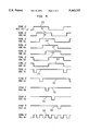
- FIG. 8 shows signals used to illustrate the operation of the clock synthesizer of FIG. 6.
- the present invention is directed to a clock synthesizer for synthesizing frequencies which are different from a reference clock frequency.
- the present invention is directed to a clock synthesizer for generating, from a single reference clock, clock signals having frequencies which are different from each other, and different from the frequency of the reference clock.
- the clock synthesizer of the present invention does not suffer from the problems that plague phase locked loop based clock synthesizers.
- FIG. 4 is a block diagram of a clock synthesizer 402 according to a preferred embodiment of the present invention.
- a reference clock (not shown), which is preferably a crystal oscillator, generates an input signal F IN (also called herein a reference clock signal), wherein the input signal F IN has a predetermined frequency.
- F IN also called herein a reference clock signal
- clock frequency requirements vary among applications.
- the value of the predetermined frequency of the input signal F IN is implementation dependent.
- the clock synthesizer 402 operates generally as follows.
- the clock synthesizer 402 generates an output signal F OUT from the input signal F IN , wherein the frequency of the output signal F OUT is usually different from the predetermined frequency of the input signal F IN . More particularly, the frequency of the output signal F OUT is an integer or non-integer multiple (or fraction) of the predetermined frequency of the input signal F IN .
- This integer or non-integer multiple (or fraction) by which the frequency of the output signal F OUT varies from the predetermined frequency of the input signal F IN may be dynamically, adjusted, such that the frequency of the output signal F OUT may be dynamically adjusted.
- the clock synthesizer 402 of the present invention synthesizes frequencies which differ from each other, and which differ from the frequency of the reference clock signal. The clock synthesizer 402 shall now be described in detail.
- the clock synthesizer 402 includes a "Divide by N” divider 404 (hereafter call the "N divider") which receives the input signal F IN .
- the N divider 404 is similar in structure and operation to the N divider 104 and the M divider 112 shown in FIG. 1, and discussed above.
- the N divider 404 operates to generate a modified input signal F IN ' from the input signal F IN , wherein the frequency of the modified input signal F IN ' is equal to the frequency of the input signal F IN divided by N.
- the N divider 404 enables the clock synthesizer 402 to synthesize a broader range of frequencies.
- the modified input signal F IN ' is transferred to a delay locked loop 408.
- Delay locked loops are generally well known, and are discussed in many publicly available documents, such as "A Monolithic CMOS 10 MHz DPLL For Burst-Mode Data” by Stanford and Leonowich (ISSCC Digest, 1990), which is herein incorporated by reference in its entirety.
- the delay locked loop 408 is similar in structure to a phase locked loop, and operates in the same way as a phase locked loop.
- a controllable delay line comprising a plurality of controllable delay elements 406 has replaced the voltage controlled oscillator (VCO) of the phase locked loop.
- VCO voltage controlled oscillator
- the problems which plague phase locked loop are due to the VCO contained therein. Since the delay locked loop 408 does not include a VCO, the delay locked loop 408 does not suffer from the problems which plague phase locked loops. Consequently, since the clock synthesizer 402 of the present invention is based on a delay locked loop, rather than a phase locked loop, the clock synthesizer 402 of the present invention does not suffer from the problems which plague phase locked loop-based clock synthesizers.
- the modified input signal F IN ' is received by a delay element 406A.
- the delay element 406A delays the modified input signal F IN ' by a quantran of time to produce a signal at a node 420, which differs in phase from the modified input signal F IN ' by the quantum of time. This is shown in FIG. 5, wherein a signal 502 represents the signal present at a node 418 (that is, the modified input signal F IN ') and a signal 504 represents the signal at the node 420 generated by the delay element 406A.
- Each delay element 406 delays an input signal which it receives by a quantum of time to generate an output signal which differs in phase from its input signal by the quantum of time. This is shown in FIG. 5, wherein a signal 506 represents the signal present at a node 422 generated by the delay element 406B, a signal 508 represents the signal present at a node 424 generated by the delay element 406C, a signal 510 represents the signal present at a node 426 generated by the delay element 406D, and a signal 512 represents the signal present at a node 428 generated by the delay element 406E.
- the quantum of time introduced by each of the delay elements 406 is the same.
- the delay elements 406 are controllable, such that the amount of delay introduced by each is adjustable.
- the delay elements 406 can be implemented in any number of ways.
- the delay elements 406 can be implemented using a combination of multiplexers, inverters, and/or registers. Persons skilled in the relevant art will find it apparent to implement controllable delay elements, particularly in light of the publicly available documents which discuss controllable delay elements, such as "A Monolithic CMOS 10 MHz DPLL For Burst-Mode Data," cited above.
- An inverter 416 inverts the modified input signal F IN '. This inverted modified input signal, which is present at a node 429, is shown in FIG. 5 as a signal 514.
- a phase detector 412 receives the signal generated by the delay element 406E and present at the node 428 (that is, the signal 512 in FIG. 5). The phase detector 412 also receives the inverted modified input signal which is present at the node 429 (that is, the signal 514 in FIG. 5).
- phase detector 412 compares the phase of the signal 512 to the phase of the signal 514 (preferably, the phase detector 412 operates to match a rising edge of the signal 512 to a rising edge of the signal 514), and generates an error voltage Ve (or, alternatively, an error current), wherein the magnitude of the error voltage Ve is proportional to the difference in phase between these two signals 512 and 514.
- the error voltage Ve is processed in a well known manner by a loop filter 414 to produce a control voltage Vc.
- the loop filter 914 is a low-pass filter which integrates the error voltage (or current) to a relatively constant control voltage Vc.
- the control voltage Vc is approximately the average value of the error voltage, Ve.
- the magnitude of the control voltage Vc is proportional to the delay through the delay elements 406A-E.
- the control voltage Vc is transferred to each of the delay elements 406, and causes the delay elements 406 to modify the amount of delay which they each introduce.
- the error voltage Ve and the control voltage Vc will correspond to a value which causes delay elements 406 to have a collective propagation delay equal to 1/2F IN '.
- the error voltage Ve When the signal 512 present at the node 428 is not equal in phase to the signal 514 present at the node 429, the error voltage Ve has a non-zero magnitude which is proportional to this phase difference.
- the loop filter 414 integrates this error voltage Ve (or error current) and modifies Vc appropriately.
- the delay elements 406 Upon receiving the control voltage Vc, the delay elements 406 modify the amount of delay which they introduce in accordance with the nonzero magnitude of the error voltage Ve. In this manner, the phase detector 412 controls the amount of delay which the delay elements 406 introduce such that the phase of the signal 512 present at the node 428 is equal to the phase of the signal 514 present at the node 429.
- the signals shown in FIG. 5 are those which are generated after the delay locked loop 408 has reached a "steady state.” That is, the signals in FIG. 5 are those which are generated after the phase detector 412 has adjusted the amount of delay introduced by the delay elements 406 such that the phase of the signal 512 is equal to the phase of the signal 5 14.
- the phase detector 412 preferably operates to match the phase of the signal 512 to the phase of the signal 514 after the passage of one half a period of the modified input signal F IN '. Consequently, the amount of time delay introduced by each of the delay elements 406 when the delay locked loop is in the "steady state" condition is represented by the following equation: 1/(2*frequency(F IN ')*X), where X is the number of delay elements 406 in the delay locked loop 408 (in the embodiment of FIG. 4, X is equal to five).
- the phase detector 412 could be implemented such that it matches the phase of the signal 512 present at the node 428 to the phase of the signal 514 present at the node 429 after other predetermined time periods, such as after the passage of one full period of the modified input signal F IN '.
- the amount of time delay introduced by each of the delay elements 406 when the delay locked loop is in the "steady state" condition is represented by the following equation: 1/(frequency(F IN ')*X).
- the signals 502-512 have the same frequency but different phases.
- the delay locked loop 408 by itself, cannot synthesize clock frequencies which are different from the frequency of the reference clock signal F IN .
- delay locked loops are used for purposes other than frequency synthesis, such as pulse shaping a transmitted wave (this operation is sometimes called “pre-distortion”).
- Conventional uses of delay locked loops are described in "A Monolithic CMOS 10 MHz DPLL For Burst-Mode Data," cited above.
- a mixing circuit 410 is used to generate, from the signals 502-512 generated by the delay locked loop 408, a clock signal 526 having a frequency which is different from the frequency of the reference clock signal F IN and which is different from the frequency of the modified reference clock signal F IN ' (signal 502).
- the mixing circuit 410 shall now be described.
- the mixing circuit 410 includes NAND gates 442,444,446, 448,450, and 460 (the bubbles at some of the inputs of these NAND gates represent inversion). These NAND gates 442, 444, 446, 448, 450, 460 are interconnected and receive the signals 502-512 generated by the delay locked loop 408 such that the mixing circuit 410 generates a clock signal 526 having a frequency which is different from the frequencies of the reference clock signal F IN and the modified reference clock signal F IN '.
- the signal 502 present at the node 418 is applied to the NAND gate 442.
- the signal 504 at the node 420 is inverted and applied to the NAND gate 442.
- the NAND gate 442 performs the well known "NAND" logical operation using these two signals to thereby produce a signal 16 (FIG. 5), which is present at a node 432, and which is applied to the NAND gate 460.
- the NAND gate 444 produces a signal 522, which is present at a node 438, and which is applied to the NAND gate 460.
- the NAND gate 446 produces a signal 518, which is present at a node 434, and which is applied to the NAND gate 460.
- the NAND gate 448 produces a signal 520, which is present at a node 436, and which is applied to the NAND gate 460.
- the NAND gate 450 produces a signal 524, which is present at a node 440, and which is applied to the NAND gate 460.
- the NAND gate 460 performs the well known "NAND" operation using these signals 432, 434, 436, 438, 440 discussed above to thereby produce a signal 526, which is present at a node 462, and which represents the output signal F OUT .
- the frequency of the output signal F OUT is five times the frequency of the modified input signal F IN '.
- mixing circuit 402 could be alternatively implemented using a combinational network different from that shown in FIG. 4.
- the structure and operation of such alternative combinational networks will be apparent to persons skilled in the relevant art.
- the N divider 404 enables the clock synthesizer 402 to synthesize a broader range of frequencies. This is the case, since the N divider 404 generates a modified input signal F IN ' from the input signal F IN , wherein the frequency of the modified input signal F IN ' is equal to the frequency of the input signal F IN divided by N.
- Table 2 illustrates the frequencies which can be synthesized for particular values of N using the clock synthesizer 402 shown in FIG. 4. For example, where N is 1, the frequency of F OUT is five times the frequency of F IN (this is the case shown in FIG. 5).
- the clock synthesizer 402 of FIG. 4 is limited relative to the phase locked loop synthesizer 102 (shown in FIG. 1 ) in the number of frequencies which it can synthesize from the reference clock frequency (that is, from the frequency of the input signal F IN ).
- the clock synthesizer 402 of FIG. 4 cannot synthesize the frequencies corresponding to M equals 3 and M equals 4 shown in Table 1. This is the case, since there are no phase transitions at the appropriate times in a five tap delay locked loop (that is, a delay locked loop having five delay elements).
- these frequencies can be synthesized using three and four tap delay locked loops (in combination with mixing circuits), since such delay locked loops produce signals having phase transitions which occur at the appropriate times. This is described in detail below.
- FIG. 6 is a block diagram of a clock synthesizer 601 according to an alternate embodiment of the present invention.
- a reference clock (not shown), which is preferably a crystal oscillator, generates an input signal, or reference clock signal, F IN .
- the clock synthesizer 601 includes a "Divide by N” divider 404 (hereafter call the “N divider") which is identical in structure and operation to the N divider 404 shown in FIG. 4.
- the N divider operates to generate a modified input signal F IN ' from the input signal F IN , wherein the frequency of the modified input signal F IN ' is equal to the frequency of the input signal F IN divided by N.
- the modified input signal F IN ' is transferred to a delay locked loop 603.
- the delay locked loop 603 shown in FIG. 6 is similar in operation and structure to the delay locked loop 408 shown in FIG. 4. The differences between these two delay locked loops 408, 603 shall now be discussed.
- the delay locked loop 603 shown in FIG. 6 includes a multiplexer 602 which is positioned between the delay elements 406C, 406D, 406E and the phase detector 412.
- the multiplexer 602 routes to the phase detector 412 either the signal output by the delay element 406C (and present at the node 424), the signal output by the delay element 406D (and present at the node 426), or the signal output by the delay element 406E (and present at the node 428).
- the phase detector 412 also receives the inverted modified input signal.
- the phase detector 412 operates to check whether the phase of the signal present at the node 428 is substantially equal to the phase of the signal present at the node 429 (for reference purposes, this is called the five tap case).
- all five of the delay elements 406 are used to ultimately produce the signal present at the node 428, wherein each of the delay elements 406 introduces a time delay of 1/(2*frequency(F IN ')*5).
- the signals produced by the delay elements 406 are shown as 504, 506, 508, 510, and 512 in FIG. 5.
- the phase detector 412 When the multiplexer 602 routes to the phase detector 412 the signal output by the delay element 406D (and present at the node 426), the phase detector 412 operates to check whether the phase of the signal present at the node 426 is substantially equal to the phase of the signal present at the node 429 (for reference purposes, this is called the four tap case). Note that only four of the delay elements 406A-406D are used to ultimately produce the signal present at the node 426, wherein each of these four delay elements 406A-406D introduces a time delay of 1/(2*frequency(F IN ')*4). In the four tap case, the signals produced by the delay elements 406A-406D are shown as 804, 806, 808, and 810 in FIG. 8.
- the phase detector 412 When the multiplexer 602 routes to the phase detector 412 the signal output by the delay element 406C (and present at the node 424), the phase detector 412 operates to check whether the phase of the signal present at the node 424 is substantially equal to the phase of the signal present at the node 429 (for reference purposes, this is called the three tap case). Note that only three of the delay elements 406A-406C are used to ultimately produce the signal present at the node 424, wherein each of these three delay elements 406A-406C introduces a time delay of 1/(2*frequency(F IN ')*3). The shape of the signals produced by the delay elements 406A-406C in the three tap case will be apparent to persons skilled in the relevant art based on the teachings contained herein.
- the phase of the signals produced in the three tap case is different than the phases of the signals produced in the four and five tap case. Consequently, frequencies which cannot be synthesized in the four and five tap cases can be synthesized in the three tap case.
- the clock synthesizer 601 includes three mixing circuits 604,608, and 410. Each of the mixing circuits 604, 608, and 410 is used to generate, from the signals generated by the delay locked loop 603, a clock signal having a frequency which is different from the frequency of the reference clock signal F IN , and which is different from the frequency of the modified reference clock signal F IN '.
- the mixing circuit 410 generates a clock signal having a frequency which is different from the frequencies of the reference clock signal F IN and the modified reference clock signal F IN '.
- the signals generated by the mixing circuits 604 and 610 are ignored (as described below).
- the mixing circuit 608 generates a clock signal having a frequency which is different from the frequencies of the reference clock signal F IN and the modified reference clock signal F IN '.
- the signals generated by the mixing circuits 604 and 410 are ignored.
- the mixing circuit 604 generates a clock signal having a frequency which is different from the frequencies of the reference clock signal F IN and the modified reference clock signal F IN '.
- the signals generated by the mixing circuits 608 and 410 are ignored.
- a multiplexer 612 receives the signals generated by the mixing circuits 604,608,410.
- the multiplexer 612 routes one of these signals to a node 614.
- This signal present at node 614 is the output signal F OUT .
- the routing functions performed by the multiplexers 602 and 612 are controlled by a single control signal 616.
- the control signal 616 is generated by a control mechanism (not shown), which determines whether the clock synthesizer 601 operates in the three tap case, the four tap case, or the five tap case.
- the control mechanism which may operate according to input from a user, preferably adjusts to the clock frequency needs of the system in which it is contained and, therefore, the control mechanism is implementation dependent.
- the control mechanism determines that the clock synthesizer 601 should operate in the three tap case, the control mechanism generates the control signal 616 such that the multiplexer 602 routes the signal present at node 424 to the phase detector 412, and such that the multiplexer 612 routes the signal generated by the mixing circuit 604 to the node 614.
- control mechanism determines that the clock synthesizer 601 should operate in the four tap case, the control mechanism generates the control signal 616 such that the multiplexer 602 routes the signal present at node 426 to the phase detector 412, and such that the multiplexer 612 routes the signal generated by the mixing circuit 608 to the node 614.
- control mechanism determines that the clock synthesizer 601 should operate in the five tap case, the control mechanism generates the control signal 616 such that the multiplexer 602 routes the signal present at node 428 to the phase detector 412, and such that the multiplexer 612 routes the signal generated by the mixing circuit 410 to the node 614.
- the mixing circuits 604, 608, and 410 shall now be described.
- the mixing circuit 410 can be implemented using various combinational networks. The structure and operation of such combinational networks will be apparent to persons skilled in the relevant art.
- One combinational network which can be used to implement the mixing circuit 410 is shown in FIG. 4 (described above).
- the mixing circuit 608 can be implemented using various combinational networks. The structure and operation of such combinational networks will be apparent to persons skilled in the relevant art.
- One combinational network which can be used to implement the mixing circuit 608 is shown in FIG. 7, and shall now be described. Recall that the signals produced by the delay elements 406A-406D during the four tap case are shown as 804, 806, 808, and 810 in FIG. 8.
- the mixing circuit 608 includes exclusive-OR gates 702, 704 and an OR gate 706. These gates 702, 704, 706 are interconnected and receive the signals present at nodes 418, 420, 422, and 424 (note that the signal present at node 426 is not used by the mixing circuit 608), such that the mixing circuit 608 generates a clock signal having a frequency which is different from the frequencies of the reference clock signal F IN and the modified reference clock signal F IN '.
- the signals present at nodes 418 and 420 are applied to the exclusive-OR gate 702.
- the exclusive-OR gate 702 performs the well known "exclusive-OR" logical operation using these two signals to thereby produce a signal 814, which is present at a node 708, and which is applied to the OR gate 610.
- the exclusive-OR gate 704 produces a signal 816, which is present at a node 7 10, and which is applied to the OR gate 610.
- the OR gate 706 performs the well known "OR" logical operation using these signals 814, 816 discussed above to thereby produce a signal 818, which is present at a node 610, and which represents the output signal F OUT during the four tap case. As apparent from FIG. 8, the frequency of F OUT is four times the frequency of F IN '.
- the mixing circuit 604 can be implemented using various combinational networks. The structure and operation of such combinational networks will be apparent to persons skilled in the relevant art.
- the mixing circuit 604 could be implemented by using the combinational network shown in FIG. 4, except that nodes 436 and 440 are forced to a high logical state in a well known manner. In this manner, the frequency of F OUT with be three times the frequency of F IN '.
- the clock synthesizer 601 can synthesize all of the frequencies shown in Table 1. Additional frequencies can be synthesized by modifying the combinational logic of the mixing circuits 4 10, 604,610 (i.e., by using larger numbers of taps, for example). Such modifications will be apparent to persons skilled in the relevant art. Note that, while the mixing circuits 410, 604, 610 are shown in FIG. 6 as receiving all of the signals produced by the DLL 603, the mixing circuits 410, 604, and 610 may process only some of these signals depending on the specific implementation.
Landscapes
- Stabilization Of Oscillater, Synchronisation, Frequency Synthesizers (AREA)
- Pulse Circuits (AREA)
Priority Applications (4)
| Application Number | Priority Date | Filing Date | Title |
|---|---|---|---|
| US08/160,107 US5463337A (en) | 1993-11-30 | 1993-11-30 | Delay locked loop based clock synthesizer using a dynamically adjustable number of delay elements therein |
| EP94308649A EP0655840A3 (de) | 1993-11-30 | 1994-11-23 | Taktgenerator nach dem "delay locked loop"-Prinzip mit einer dynamisch einstellbaren Anzahl von Verzögerungselementen. |
| KR1019940031648A KR950016009A (ko) | 1993-11-30 | 1994-11-29 | 지연-로크-루프 기반 클럭 신서사이저 |
| JP6319364A JPH07202655A (ja) | 1993-11-30 | 1994-11-30 | クロック合成器 |
Applications Claiming Priority (1)
| Application Number | Priority Date | Filing Date | Title |
|---|---|---|---|
| US08/160,107 US5463337A (en) | 1993-11-30 | 1993-11-30 | Delay locked loop based clock synthesizer using a dynamically adjustable number of delay elements therein |
Publications (1)
| Publication Number | Publication Date |
|---|---|
| US5463337A true US5463337A (en) | 1995-10-31 |
Family
ID=22575535
Family Applications (1)
| Application Number | Title | Priority Date | Filing Date |
|---|---|---|---|
| US08/160,107 Expired - Lifetime US5463337A (en) | 1993-11-30 | 1993-11-30 | Delay locked loop based clock synthesizer using a dynamically adjustable number of delay elements therein |
Country Status (4)
| Country | Link |
|---|---|
| US (1) | US5463337A (de) |
| EP (1) | EP0655840A3 (de) |
| JP (1) | JPH07202655A (de) |
| KR (1) | KR950016009A (de) |
Cited By (103)
| Publication number | Priority date | Publication date | Assignee | Title |
|---|---|---|---|---|
| US5629651A (en) * | 1994-08-12 | 1997-05-13 | Nec Corporation | Phase lock loop having a reduced synchronization transfer period |
| US5646564A (en) * | 1994-09-02 | 1997-07-08 | Xilinx, Inc. | Phase-locked delay loop for clock correction |
| US5646519A (en) * | 1995-06-07 | 1997-07-08 | Symmetricom, Inc. | Digital phase detector employing a digitally controllable delay line |
| US5654659A (en) * | 1994-02-28 | 1997-08-05 | Nec Corporation | Scan circuit having a reduced clock signal delay |
| DE19634181A1 (de) * | 1996-02-15 | 1997-08-21 | Mitsubishi Electric Corp | Variable Verzögerungsschaltung sowie Ringoszillator und variable Impulsbreitenschaltung, die diese variable Verzögerungsschaltung verwenden |
| WO1997040576A1 (en) * | 1996-04-25 | 1997-10-30 | Credence Systems Corporation | Frequency multiplier |
| US5786715A (en) * | 1996-06-21 | 1998-07-28 | Sun Microsystems, Inc. | Programmable digital frequency multiplier |
| US5801559A (en) * | 1995-09-06 | 1998-09-01 | Mitsubishi Denki Kabushiki Kaisha | Clock generating circuit, PLL circuit, semiconductor device, and methods for designing and making the clock generating circuit |
| US5805003A (en) * | 1995-11-02 | 1998-09-08 | Cypress Semiconductor Corp. | Clock frequency synthesis using delay-locked loop |
| US5815016A (en) * | 1994-09-02 | 1998-09-29 | Xilinx, Inc. | Phase-locked delay loop for clock correction |
| US5901190A (en) * | 1995-12-27 | 1999-05-04 | Samsung Electronics, Co., Ltd. | Digital delay locked loop circuit using synchronous delay line |
| US5914963A (en) * | 1996-06-21 | 1999-06-22 | Compaq Computer Corporation | Clock skew reduction |
| US5955902A (en) * | 1996-04-01 | 1999-09-21 | Kabushiki Kaisha Toshiba | Frequency multiplier using a voltage controlled delay circuit |
| US5959481A (en) * | 1997-02-18 | 1999-09-28 | Rambus Inc. | Bus driver circuit including a slew rate indicator circuit having a one shot circuit |
| WO1999056393A1 (en) * | 1998-04-30 | 1999-11-04 | Intel Corporation | Method and apparatus for varying a clock frequency on a phase by phase basis |
| WO1999059053A1 (en) * | 1998-05-13 | 1999-11-18 | Intel Corporation | Multiple synthesizer based timing signal generation scheme |
| US5990715A (en) * | 1996-11-19 | 1999-11-23 | Fujitsu Limited | Semiconductor integrated circuit using a synchronized control signal |
| US6005420A (en) * | 1996-04-01 | 1999-12-21 | Kabushiki Kaisha Toshiba | Frequency multiplying circuit having a greater multiplying ratio |
| US6020773A (en) * | 1997-11-14 | 2000-02-01 | Mitsubishi Denki Kabushiki Kaisha | Clock signal generator for generating a plurality of clock signals with different phases, and clock phase controller using the same |
| US6037813A (en) * | 1997-01-20 | 2000-03-14 | Fujitsu Limited | Semiconductor device capable of selecting operation mode based on clock frequency |
| US6043694A (en) * | 1998-06-24 | 2000-03-28 | Siemens Aktiengesellschaft | Lock arrangement for a calibrated DLL in DDR SDRAM applications |
| US6052748A (en) * | 1997-03-18 | 2000-04-18 | Edwin A. Suominen | Analog reconstruction of asynchronously sampled signals from a digital signal processor |
| US6055287A (en) * | 1998-05-26 | 2000-04-25 | Mcewan; Thomas E. | Phase-comparator-less delay locked loop |
| US6100735A (en) * | 1998-11-19 | 2000-08-08 | Centillium Communications, Inc. | Segmented dual delay-locked loop for precise variable-phase clock generation |
| US6137334A (en) * | 1998-07-06 | 2000-10-24 | Micron Technology, Inc. | Logic circuit delay stage and delay line utilizing same |
| US6208183B1 (en) * | 1999-04-30 | 2001-03-27 | Conexant Systems, Inc. | Gated delay-locked loop for clock generation applications |
| US6232813B1 (en) | 1998-10-19 | 2001-05-15 | Samsung Electronics Co., Ltd. | Phase locked loop integrated circuits having fuse-enabled and fuse-disabled delay devices therein |
| US6282210B1 (en) | 1998-08-12 | 2001-08-28 | Staktek Group L.P. | Clock driver with instantaneously selectable phase and method for use in data communication systems |
| US6329854B1 (en) | 1998-09-02 | 2001-12-11 | Samsung Electronics Co., Ltd. | Phase locked loop integrated circuits having dynamic phase locking characteristics and methods of operating same |
| US6369627B1 (en) * | 1999-10-12 | 2002-04-09 | Fujitsu Limited | Delay circuit and semiconductor integrated circuit having same |
| US6404250B1 (en) | 2001-03-28 | 2002-06-11 | Infineon Technologies Richmond, Lp | On-chip circuits for high speed memory testing with a slow memory tester |
| US6415008B1 (en) | 1998-12-15 | 2002-07-02 | BéCHADE ROLAND ALBERT | Digital signal multiplier |
| US6421784B1 (en) | 1999-03-05 | 2002-07-16 | International Business Machines Corporation | Programmable delay circuit having a fine delay element selectively receives input signal and output signal of coarse delay element |
| US6441659B1 (en) * | 1999-04-30 | 2002-08-27 | Mosaid Technologies Incorporated | Frequency-doubling delay locked loop |
| US6441666B1 (en) * | 2000-07-20 | 2002-08-27 | Silicon Graphics, Inc. | System and method for generating clock signals |
| US6448834B2 (en) * | 2000-03-10 | 2002-09-10 | Konica Corporation | Clock generating device |
| US20020163986A1 (en) * | 1999-03-01 | 2002-11-07 | Harrison Ronnie M. | Method and apparatus for generating a phase dependent control signal |
| US6486722B2 (en) * | 1999-11-22 | 2002-11-26 | Mitsubishi Denki Kabushiki Kaisha | Semiconductor device including a control signal generation circuit allowing reduction in size |
| US6594772B1 (en) * | 2000-01-14 | 2003-07-15 | Hewlett-Packard Development Company, L.P. | Clock distribution circuitry to different nodes on integrated circuit with clock coupling circuitry to maintain predetermined phase relation between output and input of adjacent nodes |
| US20030137333A1 (en) * | 2001-12-25 | 2003-07-24 | Minoru Kozaki | Multiphase-clock processing circuit and clock multiplying circuit |
| US6603337B2 (en) * | 2000-12-29 | 2003-08-05 | Hynix Semiconductor Inc. | Duty cycle correction circuit |
| US6625242B1 (en) * | 1999-01-27 | 2003-09-23 | Samsung Electronics Co., Ltd. | Delay locked loops and methods that shift the phase of a delayed clock signal based on a reference phase value |
| US20030210602A1 (en) * | 1999-11-01 | 2003-11-13 | Hynix Semiconductor, Inc. | Delay locked loop for use in synchronous dynamic random access memory |
| US20040059533A1 (en) * | 2002-09-25 | 2004-03-25 | Parrish Gregory C. | Method and apparatus for calibration of a delay element |
| US20040066222A1 (en) * | 2002-10-04 | 2004-04-08 | Mcwilliams John | Non-iterative introduction of phase delay into signal without feedback |
| US6727734B2 (en) | 2001-08-29 | 2004-04-27 | Micron Technology, Inc. | Variable delay circuit and method, and delay locked loop, memory device and computer system using same |
| US6727764B2 (en) * | 2002-03-08 | 2004-04-27 | Sirific Wireless Corporation | Generation of virtual local oscillator inputs for use in direct conversion radio systems |
| US20040109514A1 (en) * | 2000-02-17 | 2004-06-10 | Rahul Magoon | Method and apparatus for multiple phase splitting for dual band IQ subharmonic mixer |
| US20040130371A1 (en) * | 2003-01-08 | 2004-07-08 | Roy Aninda K. | Unity gain interpolator for delay locked loops |
| US6765976B1 (en) | 2000-03-29 | 2004-07-20 | G-Link Technology | Delay-locked loop for differential clock signals |
| US6774691B2 (en) | 2003-01-07 | 2004-08-10 | Infineon Technologies Ag | High resolution interleaved delay chain |
| US6777990B2 (en) * | 2002-03-19 | 2004-08-17 | Infineon Technologies Ag | Delay lock loop having an edge detector and fixed delay |
| US20040179640A1 (en) * | 2003-03-12 | 2004-09-16 | Infineon Technologies North America Corp. | Multiple delay locked loop integration system and method |
| US6795514B2 (en) | 2000-02-28 | 2004-09-21 | Zarlink Semiconductor Inc. | Integrated data clock extractor |
| US20040227550A1 (en) * | 2003-05-12 | 2004-11-18 | Byun Gyung-Su | Semiconductor device having delay-locked loop and test method thereof |
| US20050017774A1 (en) * | 2001-05-29 | 2005-01-27 | Stmicroelectronics, Inc. | Precision closed loop delay line for wide frequency data recovery |
| US6885228B2 (en) | 2002-10-02 | 2005-04-26 | Hewlett-Packard Development Company, L.P. | Non-iterative signal synchronization |
| US20050110539A1 (en) * | 2003-11-26 | 2005-05-26 | Micron Technology, Inc. | Digital delay-locked loop circuits with hierarchical delay adjustment |
| US20050110554A1 (en) * | 2003-11-21 | 2005-05-26 | Micron Technology, Inc. | Digital phase mixers with enhanced speed |
| US20050127964A1 (en) * | 2003-12-11 | 2005-06-16 | Micron Technology, Inc. | Digital frequency-multiplying DLLs |
| US20050134337A1 (en) * | 2003-12-22 | 2005-06-23 | Micron Technology, Inc. | Clock signal distribution with reduced parasitic loading effects |
| RU2260905C1 (ru) * | 2004-02-10 | 2005-09-20 | Пензенский технологический институт | Генератор импульсов с процентным фазовым шумом |
| US6954097B2 (en) * | 1997-06-20 | 2005-10-11 | Micron Technology, Inc. | Method and apparatus for generating a sequence of clock signals |
| US20050253631A1 (en) * | 2004-05-12 | 2005-11-17 | Chul-Soo Kim | Internal signal replication device and method |
| US20050265506A1 (en) * | 1994-10-06 | 2005-12-01 | Mosaid Technologies, Inc. | Delay locked loop implementation in a synchronous dynamic random access memory |
| US6975695B1 (en) * | 2001-04-30 | 2005-12-13 | Cypress Semiconductor Corp. | Circuit for correction of differential signal path delays in a PLL |
| US7009434B2 (en) | 2003-12-12 | 2006-03-07 | Micron Technology, Inc. | Generating multi-phase clock signals using hierarchical delays |
| US7085975B2 (en) | 1998-09-03 | 2006-08-01 | Micron Technology, Inc. | Method and apparatus for generating expect data from a captured bit pattern, and memory device using same |
| US7098710B1 (en) * | 2003-11-21 | 2006-08-29 | Xilinx, Inc. | Multi-speed delay-locked loop |
| US20060232315A1 (en) * | 2005-04-15 | 2006-10-19 | Seong-Hoon Lee | Variable delay line with multiple hierarchy |
| US7159092B2 (en) | 2001-06-28 | 2007-01-02 | Micron Technology, Inc. | Method and system for adjusting the timing offset between a clock signal and respective digital signals transmitted along with that clock signal, and memory device and computer system using same |
| US20070011483A1 (en) * | 2005-06-01 | 2007-01-11 | Feng Lin | Delay-lock loop and method adapting itself to operate over a wide frequency range |
| US7168027B2 (en) | 2003-06-12 | 2007-01-23 | Micron Technology, Inc. | Dynamic synchronization of data capture on an optical or other high speed communications link |
| KR100715845B1 (ko) * | 2001-02-17 | 2007-05-10 | 삼성전자주식회사 | 위상혼합기 및 이를 이용한 다중위상 발생기 |
| US7221202B1 (en) * | 2004-09-15 | 2007-05-22 | Cypress Semiconductor Corporation | Delay-locked loop with reduced susceptibility to false lock |
| US20070118251A1 (en) * | 2005-11-08 | 2007-05-24 | Jui-Hsing Tseng | Systems and methods for automatically eliminating imbalance between signals |
| US7236028B1 (en) * | 2005-07-22 | 2007-06-26 | National Semiconductor Corporation | Adaptive frequency variable delay-locked loop |
| US20070200609A1 (en) * | 2006-02-28 | 2007-08-30 | Samsung Electronics Co., Ltd. | Integrated circuit devices generating a plurality of drowsy clock signals having different phases |
| US20080018372A1 (en) * | 2004-09-17 | 2008-01-24 | Nec Corporation | Clock Generating Circuit and Clock Generating Method |
| US20080074151A1 (en) * | 2006-09-22 | 2008-03-27 | Samsung Electronics Co., Ltd. | Dual-edge-triggered, clock-gated logic circuit and method |
| US20080116951A1 (en) * | 2006-11-22 | 2008-05-22 | Zuoguo Wu | Frequency multiplying delay-locked loop |
| USRE40552E1 (en) | 1990-04-06 | 2008-10-28 | Mosaid Technologies, Inc. | Dynamic random access memory using imperfect isolating transistors |
| US20080276116A1 (en) * | 2005-06-01 | 2008-11-06 | Tobias Bjerregaard | Method and an Apparatus for Providing Timing Signals to a Number of Circuits, an Integrated Circuit and a Node |
| US7453297B1 (en) * | 2005-08-05 | 2008-11-18 | Xilinx, Inc. | Method of and circuit for deskewing clock signals in an integrated circuit |
| US7453301B1 (en) | 2005-08-05 | 2008-11-18 | Xilinx, Inc. | Method of and circuit for phase shifting a clock signal |
| US7461286B2 (en) | 2003-10-27 | 2008-12-02 | Micron Technology, Inc. | System and method for using a learning sequence to establish communications on a high-speed nonsynchronous interface in the absence of clock forwarding |
| US20080303575A1 (en) * | 2007-06-05 | 2008-12-11 | Seiko Epson Corporation | Pulse generating circuit and uwb communication system |
| US20090009220A1 (en) * | 2006-02-09 | 2009-01-08 | Fujitsu Limited | Signal generating apparatus, periodic-signal observing system, integrated circuit, periodic-signal observing method, and method of testing integrated circuit |
| US20090116602A1 (en) * | 2007-11-07 | 2009-05-07 | Micron Technology, Inc. | High speed, wide frequency-range, digital phase mixer and methods of operation |
| US7535749B2 (en) | 1990-04-06 | 2009-05-19 | Mosaid Technologies, Inc. | Dynamic memory word line driver scheme |
| US7564283B1 (en) | 1998-06-22 | 2009-07-21 | Xilinx, Inc. | Automatic tap delay calibration for precise digital phase shift |
| US20090195279A1 (en) * | 2008-02-05 | 2009-08-06 | Feng Lin | Delay locked loop circuit and method |
| US20100007389A1 (en) * | 2008-07-09 | 2010-01-14 | Yi Li | Multiple frequency synchronized phase clock generator |
| US7675332B1 (en) * | 2007-01-31 | 2010-03-09 | Altera Corporation | Fractional delay-locked loops |
| US7675336B1 (en) * | 2004-12-17 | 2010-03-09 | Altera Corporation | Clock duty cycle recovery circuit |
| US20120182053A1 (en) * | 2011-01-18 | 2012-07-19 | Qualcomm Incorporated | Half cycle delay locked loop |
| US20130088268A1 (en) * | 2011-10-05 | 2013-04-11 | Tinnotek Inc. | Multi-Phase Clock Generation System and Clock Calibration Method Thereof |
| US8692602B2 (en) * | 2012-07-30 | 2014-04-08 | Taiwan Semiconductor Manufacturing Company, Ltd. | Method and apparatus of digital control delay line |
| US10496127B1 (en) * | 2018-06-04 | 2019-12-03 | Linear Technology Holding Llc | Multi-chip timing alignment to a common reference signal |
| US10720928B1 (en) | 2019-03-12 | 2020-07-21 | United States Of America As Represented By The Secretary Of The Air Force | Frequency agile modulator |
| US12301240B2 (en) * | 2022-06-16 | 2025-05-13 | Stmicroelectronics S.R.L. | Clock generator circuit, corresponding device and method |
| US12652054B1 (en) * | 2024-12-05 | 2026-06-09 | Qualcomm Incorporated | Current starved delay line bandwidth across process corners |
| RU2864199C1 (ru) * | 2026-02-05 | 2026-06-18 | Акционерное общество "Аэроприбор-Восход" | Устройство слежения за характерной точкой импульсного радиосигнала |
Families Citing this family (15)
| Publication number | Priority date | Publication date | Assignee | Title |
|---|---|---|---|---|
| US5614868A (en) * | 1995-10-24 | 1997-03-25 | Vlsi Technology, Inc. | Phase locked loop having voltage controlled oscillator utilizing combinational logic |
| US5786732A (en) * | 1995-10-24 | 1998-07-28 | Vlsi Technology, Inc. | Phase locked loop circuitry including a multiple frequency output voltage controlled oscillator circuit |
| US6028903A (en) * | 1997-03-31 | 2000-02-22 | Sun Microsystems, Inc. | Delay lock loop with transition recycling for clock recovery of NRZ run-length encoded serial data signals |
| US5889435A (en) * | 1997-06-30 | 1999-03-30 | Sun Microsystems, Inc. | On-chip PLL phase and jitter self-test circuit |
| KR100483052B1 (ko) * | 1997-12-24 | 2005-08-25 | 주식회사 하이닉스반도체 | 위상지연회로 |
| US6289068B1 (en) | 1998-06-22 | 2001-09-11 | Xilinx, Inc. | Delay lock loop with clock phase shifter |
| US6064272A (en) * | 1998-07-01 | 2000-05-16 | Conexant Systems, Inc. | Phase interpolated fractional-N frequency synthesizer with on-chip tuning |
| GB2376821B (en) * | 1998-12-30 | 2003-04-09 | Hyundai Electronics Ind | Delayed locked loop clock generator using delay-pulse-delay |
| KR100303777B1 (ko) | 1998-12-30 | 2001-11-02 | 박종섭 | 지연-펄스-지연을 이용한 지연고정루프 클록발생기 |
| JP2003050738A (ja) * | 2001-08-03 | 2003-02-21 | Elpida Memory Inc | キャリブレーション方法及びメモリシステム |
| US7154978B2 (en) * | 2001-11-02 | 2006-12-26 | Motorola, Inc. | Cascaded delay locked loop circuit |
| US7157951B1 (en) | 2004-04-30 | 2007-01-02 | Xilinx, Inc. | Digital clock manager capacitive trim unit |
| US7038519B1 (en) | 2004-04-30 | 2006-05-02 | Xilinx, Inc. | Digital clock manager having cascade voltage switch logic clock paths |
| US7046052B1 (en) | 2004-04-30 | 2006-05-16 | Xilinx, Inc. | Phase matched clock divider |
| US7482885B2 (en) * | 2005-12-29 | 2009-01-27 | Orca Systems, Inc. | Method of frequency synthesis for fast switching |
Citations (3)
| Publication number | Priority date | Publication date | Assignee | Title |
|---|---|---|---|---|
| US5049766A (en) * | 1989-10-27 | 1991-09-17 | Ncr Corporation | Delay measuring circuit |
| US5120990A (en) * | 1990-06-29 | 1992-06-09 | Analog Devices, Inc. | Apparatus for generating multiple phase clock signals and phase detector therefor |
| US5260608A (en) * | 1990-02-06 | 1993-11-09 | Bull, S.A. | Phase-locked loop and resulting frequency multiplier |
-
1993
- 1993-11-30 US US08/160,107 patent/US5463337A/en not_active Expired - Lifetime
-
1994
- 1994-11-23 EP EP94308649A patent/EP0655840A3/de not_active Withdrawn
- 1994-11-29 KR KR1019940031648A patent/KR950016009A/ko not_active Ceased
- 1994-11-30 JP JP6319364A patent/JPH07202655A/ja active Pending
Patent Citations (3)
| Publication number | Priority date | Publication date | Assignee | Title |
|---|---|---|---|---|
| US5049766A (en) * | 1989-10-27 | 1991-09-17 | Ncr Corporation | Delay measuring circuit |
| US5260608A (en) * | 1990-02-06 | 1993-11-09 | Bull, S.A. | Phase-locked loop and resulting frequency multiplier |
| US5120990A (en) * | 1990-06-29 | 1992-06-09 | Analog Devices, Inc. | Apparatus for generating multiple phase clock signals and phase detector therefor |
Non-Patent Citations (4)
| Title |
|---|
| Floyd M. Gardner, Charge Pump Phase Lock Loops, Nov., 1980, pp. 1849 1858. * |
| Floyd M. Gardner, Charge-Pump Phase-Lock Loops, Nov., 1980, pp. 1849-1858. |
| Jeff Sonntag, Robert Leonowich, Session 11: High Speed Communication IC s; FAM 11.5: A Monolithic CMOS 10MHz DPLL for Burst Mode Data Retiming, 1900 IEE International Solid State Circuits Conference (ISSCC 90) Feb. 16, 1990. pp. 194 195. * |
| Jeff Sonntag, Robert Leonowich, Session 11: High-Speed Communication IC's; FAM 11.5: A Monolithic CMOS 10MHz DPLL for Burst-Mode Data Retiming,1900 IEE International Solid-State Circuits Conference (ISSCC 90) Feb. 16, 1990. pp. 194-195. |
Cited By (194)
| Publication number | Priority date | Publication date | Assignee | Title |
|---|---|---|---|---|
| US7535749B2 (en) | 1990-04-06 | 2009-05-19 | Mosaid Technologies, Inc. | Dynamic memory word line driver scheme |
| US8023314B2 (en) | 1990-04-06 | 2011-09-20 | Mosaid Technologies Incorporated | Dynamic memory word line driver scheme |
| USRE40552E1 (en) | 1990-04-06 | 2008-10-28 | Mosaid Technologies, Inc. | Dynamic random access memory using imperfect isolating transistors |
| US5654659A (en) * | 1994-02-28 | 1997-08-05 | Nec Corporation | Scan circuit having a reduced clock signal delay |
| US5629651A (en) * | 1994-08-12 | 1997-05-13 | Nec Corporation | Phase lock loop having a reduced synchronization transfer period |
| US5815016A (en) * | 1994-09-02 | 1998-09-29 | Xilinx, Inc. | Phase-locked delay loop for clock correction |
| US5646564A (en) * | 1994-09-02 | 1997-07-08 | Xilinx, Inc. | Phase-locked delay loop for clock correction |
| US7599246B2 (en) * | 1994-10-06 | 2009-10-06 | Mosaid Technologies, Inc. | Delay locked loop implementation in a synchronous dynamic random access memory |
| US20090316514A1 (en) * | 1994-10-06 | 2009-12-24 | Foss Richard C | Delay Locked Loop Implementation in a Synchronous Dynamic Random Access Memory |
| US8638638B2 (en) | 1994-10-06 | 2014-01-28 | Mosaid Technologies Incorporated | Delay locked loop implementation in a synchronous dynamic random access memory |
| US20050265506A1 (en) * | 1994-10-06 | 2005-12-01 | Mosaid Technologies, Inc. | Delay locked loop implementation in a synchronous dynamic random access memory |
| US8369182B2 (en) * | 1994-10-06 | 2013-02-05 | Mosaid Technologies Incorporated | Delay locked loop implementation in a synchronous dynamic random access memory |
| US5646519A (en) * | 1995-06-07 | 1997-07-08 | Symmetricom, Inc. | Digital phase detector employing a digitally controllable delay line |
| US5801559A (en) * | 1995-09-06 | 1998-09-01 | Mitsubishi Denki Kabushiki Kaisha | Clock generating circuit, PLL circuit, semiconductor device, and methods for designing and making the clock generating circuit |
| US5805003A (en) * | 1995-11-02 | 1998-09-08 | Cypress Semiconductor Corp. | Clock frequency synthesis using delay-locked loop |
| US5901190A (en) * | 1995-12-27 | 1999-05-04 | Samsung Electronics, Co., Ltd. | Digital delay locked loop circuit using synchronous delay line |
| DE19634181A1 (de) * | 1996-02-15 | 1997-08-21 | Mitsubishi Electric Corp | Variable Verzögerungsschaltung sowie Ringoszillator und variable Impulsbreitenschaltung, die diese variable Verzögerungsschaltung verwenden |
| US6005420A (en) * | 1996-04-01 | 1999-12-21 | Kabushiki Kaisha Toshiba | Frequency multiplying circuit having a greater multiplying ratio |
| US5955902A (en) * | 1996-04-01 | 1999-09-21 | Kabushiki Kaisha Toshiba | Frequency multiplier using a voltage controlled delay circuit |
| WO1997040576A1 (en) * | 1996-04-25 | 1997-10-30 | Credence Systems Corporation | Frequency multiplier |
| US5914963A (en) * | 1996-06-21 | 1999-06-22 | Compaq Computer Corporation | Clock skew reduction |
| US5786715A (en) * | 1996-06-21 | 1998-07-28 | Sun Microsystems, Inc. | Programmable digital frequency multiplier |
| US5990715A (en) * | 1996-11-19 | 1999-11-23 | Fujitsu Limited | Semiconductor integrated circuit using a synchronized control signal |
| US6037813A (en) * | 1997-01-20 | 2000-03-14 | Fujitsu Limited | Semiconductor device capable of selecting operation mode based on clock frequency |
| US5959481A (en) * | 1997-02-18 | 1999-09-28 | Rambus Inc. | Bus driver circuit including a slew rate indicator circuit having a one shot circuit |
| US6052748A (en) * | 1997-03-18 | 2000-04-18 | Edwin A. Suominen | Analog reconstruction of asynchronously sampled signals from a digital signal processor |
| US6954097B2 (en) * | 1997-06-20 | 2005-10-11 | Micron Technology, Inc. | Method and apparatus for generating a sequence of clock signals |
| US7415404B2 (en) | 1997-06-20 | 2008-08-19 | Micron Technology, Inc. | Method and apparatus for generating a sequence of clock signals |
| US7889593B2 (en) | 1997-06-20 | 2011-02-15 | Round Rock Research, Llc | Method and apparatus for generating a sequence of clock signals |
| US8565008B2 (en) | 1997-06-20 | 2013-10-22 | Round Rock Research, Llc | Method and apparatus for generating a sequence of clock signals |
| US6020773A (en) * | 1997-11-14 | 2000-02-01 | Mitsubishi Denki Kabushiki Kaisha | Clock signal generator for generating a plurality of clock signals with different phases, and clock phase controller using the same |
| WO1999056393A1 (en) * | 1998-04-30 | 1999-11-04 | Intel Corporation | Method and apparatus for varying a clock frequency on a phase by phase basis |
| US6127858A (en) * | 1998-04-30 | 2000-10-03 | Intel Corporation | Method and apparatus for varying a clock frequency on a phase by phase basis |
| GB2353156B (en) * | 1998-04-30 | 2003-04-16 | Intel Corp | Method and apparatus for varying a clock frequency on a phase by phase basis |
| GB2353156A (en) * | 1998-04-30 | 2001-02-14 | Intel Corp | Method and apparatus for varying a clock frequency on a phase by phase basis |
| GB2353618A (en) * | 1998-05-13 | 2001-02-28 | Intel Corp | Multiple synthesizer based timing signal generation scheme |
| WO1999059053A1 (en) * | 1998-05-13 | 1999-11-18 | Intel Corporation | Multiple synthesizer based timing signal generation scheme |
| US6172937B1 (en) | 1998-05-13 | 2001-01-09 | Intel Corporation | Multiple synthesizer based timing signal generation scheme |
| GB2353618B (en) * | 1998-05-13 | 2003-04-30 | Intel Corp | Multiple synthesizer based timing signal generation scheme |
| US6055287A (en) * | 1998-05-26 | 2000-04-25 | Mcewan; Thomas E. | Phase-comparator-less delay locked loop |
| US7564283B1 (en) | 1998-06-22 | 2009-07-21 | Xilinx, Inc. | Automatic tap delay calibration for precise digital phase shift |
| US6043694A (en) * | 1998-06-24 | 2000-03-28 | Siemens Aktiengesellschaft | Lock arrangement for a calibrated DLL in DDR SDRAM applications |
| US6392458B1 (en) | 1998-07-06 | 2002-05-21 | Micron Technology, Inc. | Method and apparatus for digital delay locked loop circuits |
| US6359482B1 (en) | 1998-07-06 | 2002-03-19 | Micron Technology, Inc. | Method and apparatus for digital delay locked loop circuits |
| US6137334A (en) * | 1998-07-06 | 2000-10-24 | Micron Technology, Inc. | Logic circuit delay stage and delay line utilizing same |
| US6282210B1 (en) | 1998-08-12 | 2001-08-28 | Staktek Group L.P. | Clock driver with instantaneously selectable phase and method for use in data communication systems |
| DE19912967B4 (de) * | 1998-09-02 | 2008-01-24 | Samsung Electronics Co., Ltd., Suwon | Verzögerungsregelkreisschaltung und Steuerverfahren hierfür |
| US6329854B1 (en) | 1998-09-02 | 2001-12-11 | Samsung Electronics Co., Ltd. | Phase locked loop integrated circuits having dynamic phase locking characteristics and methods of operating same |
| US7657813B2 (en) | 1998-09-03 | 2010-02-02 | Micron Technology, Inc. | Method and apparatus for generating expect data from a captured bit pattern, and memory device using same |
| US7954031B2 (en) | 1998-09-03 | 2011-05-31 | Round Rock Research, Llc | Method and apparatus for generating expect data from a captured bit pattern, and memory device using same |
| US7085975B2 (en) | 1998-09-03 | 2006-08-01 | Micron Technology, Inc. | Method and apparatus for generating expect data from a captured bit pattern, and memory device using same |
| US7373575B2 (en) | 1998-09-03 | 2008-05-13 | Micron Technology, Inc. | Method and apparatus for generating expect data from a captured bit pattern, and memory device using same |
| US6232813B1 (en) | 1998-10-19 | 2001-05-15 | Samsung Electronics Co., Ltd. | Phase locked loop integrated circuits having fuse-enabled and fuse-disabled delay devices therein |
| US6100735A (en) * | 1998-11-19 | 2000-08-08 | Centillium Communications, Inc. | Segmented dual delay-locked loop for precise variable-phase clock generation |
| US6415008B1 (en) | 1998-12-15 | 2002-07-02 | BéCHADE ROLAND ALBERT | Digital signal multiplier |
| US6625242B1 (en) * | 1999-01-27 | 2003-09-23 | Samsung Electronics Co., Ltd. | Delay locked loops and methods that shift the phase of a delayed clock signal based on a reference phase value |
| US8107580B2 (en) | 1999-03-01 | 2012-01-31 | Round Rock Research, Llc | Method and apparatus for generating a phase dependent control signal |
| US7016451B2 (en) | 1999-03-01 | 2006-03-21 | Micron Technology, Inc. | Method and apparatus for generating a phase dependent control signal |
| US20020163986A1 (en) * | 1999-03-01 | 2002-11-07 | Harrison Ronnie M. | Method and apparatus for generating a phase dependent control signal |
| US7602876B2 (en) | 1999-03-01 | 2009-10-13 | Micron Technology, Inc. | Method and apparatus for generating a phase dependent control signal |
| US8433023B2 (en) | 1999-03-01 | 2013-04-30 | Round Rock Research, Llc | Method and apparatus for generating a phase dependent control signal |
| US7418071B2 (en) | 1999-03-01 | 2008-08-26 | Micron Technology, Inc. | Method and apparatus for generating a phase dependent control signal |
| US6931086B2 (en) | 1999-03-01 | 2005-08-16 | Micron Technology, Inc. | Method and apparatus for generating a phase dependent control signal |
| US6421784B1 (en) | 1999-03-05 | 2002-07-16 | International Business Machines Corporation | Programmable delay circuit having a fine delay element selectively receives input signal and output signal of coarse delay element |
| US7116141B2 (en) | 1999-04-30 | 2006-10-03 | Mosaid Technologies Incorporated | Frequency-doubling delay locked loop |
| US6441659B1 (en) * | 1999-04-30 | 2002-08-27 | Mosaid Technologies Incorporated | Frequency-doubling delay locked loop |
| US8754687B2 (en) | 1999-04-30 | 2014-06-17 | Conversant Intellectual Property Management Inc. | Frequency-doubling delay locked loop |
| US7456666B2 (en) | 1999-04-30 | 2008-11-25 | Mosaid Technologies, Inc. | Frequency-doubling delay locked loop |
| US20090039931A1 (en) * | 1999-04-30 | 2009-02-12 | Mosaid Technologies, Inc. | Frequency-doubling delay locked loop |
| US6208183B1 (en) * | 1999-04-30 | 2001-03-27 | Conexant Systems, Inc. | Gated delay-locked loop for clock generation applications |
| DE10084500B3 (de) * | 1999-04-30 | 2014-02-13 | Mosaid Technologies Inc. | Frequenzvervielfachende Delay Locked Loop |
| US8283959B2 (en) | 1999-04-30 | 2012-10-09 | Mosaid Technologies Incorporated | Frequency-doubling delay locked loop |
| US20100225370A1 (en) * | 1999-04-30 | 2010-09-09 | Mosaid Technologies Incorporated | Frequency-Doubling Delay Locked Loop |
| US8558593B2 (en) | 1999-04-30 | 2013-10-15 | Mosaid Technologies Incorporated | Frequency-doubling delay locked loop |
| US20030042947A1 (en) * | 1999-04-30 | 2003-03-06 | Demone Paul W. | Frequency-doubling delay locked loop |
| US7746136B2 (en) | 1999-04-30 | 2010-06-29 | Mosaid Technologies Incorporated | Frequency-doubling delay locked loop |
| US20060261866A1 (en) * | 1999-04-30 | 2006-11-23 | Demone Paul W | Frequency-doubling delay locked loop |
| US6369627B1 (en) * | 1999-10-12 | 2002-04-09 | Fujitsu Limited | Delay circuit and semiconductor integrated circuit having same |
| US7230875B2 (en) * | 1999-11-01 | 2007-06-12 | Hynix Semiconductor, Inc. | Delay locked loop for use in synchronous dynamic random access memory |
| US20030210602A1 (en) * | 1999-11-01 | 2003-11-13 | Hynix Semiconductor, Inc. | Delay locked loop for use in synchronous dynamic random access memory |
| US6486722B2 (en) * | 1999-11-22 | 2002-11-26 | Mitsubishi Denki Kabushiki Kaisha | Semiconductor device including a control signal generation circuit allowing reduction in size |
| US6594772B1 (en) * | 2000-01-14 | 2003-07-15 | Hewlett-Packard Development Company, L.P. | Clock distribution circuitry to different nodes on integrated circuit with clock coupling circuitry to maintain predetermined phase relation between output and input of adjacent nodes |
| US20040109514A1 (en) * | 2000-02-17 | 2004-06-10 | Rahul Magoon | Method and apparatus for multiple phase splitting for dual band IQ subharmonic mixer |
| US7145963B2 (en) * | 2000-02-17 | 2006-12-05 | Skyworks Solutions, Inc. | Method and apparatus for multiple phase splitting for dual band IQ subharmonic mixer drive chains |
| US6795514B2 (en) | 2000-02-28 | 2004-09-21 | Zarlink Semiconductor Inc. | Integrated data clock extractor |
| US6448834B2 (en) * | 2000-03-10 | 2002-09-10 | Konica Corporation | Clock generating device |
| US6765976B1 (en) | 2000-03-29 | 2004-07-20 | G-Link Technology | Delay-locked loop for differential clock signals |
| US6441666B1 (en) * | 2000-07-20 | 2002-08-27 | Silicon Graphics, Inc. | System and method for generating clock signals |
| US6603337B2 (en) * | 2000-12-29 | 2003-08-05 | Hynix Semiconductor Inc. | Duty cycle correction circuit |
| KR100715845B1 (ko) * | 2001-02-17 | 2007-05-10 | 삼성전자주식회사 | 위상혼합기 및 이를 이용한 다중위상 발생기 |
| US6404250B1 (en) | 2001-03-28 | 2002-06-11 | Infineon Technologies Richmond, Lp | On-chip circuits for high speed memory testing with a slow memory tester |
| US6975695B1 (en) * | 2001-04-30 | 2005-12-13 | Cypress Semiconductor Corp. | Circuit for correction of differential signal path delays in a PLL |
| US6985016B2 (en) * | 2001-05-29 | 2006-01-10 | Stmicroelectronics, Inc. | Precision closed loop delay line for wide frequency data recovery |
| US20050017774A1 (en) * | 2001-05-29 | 2005-01-27 | Stmicroelectronics, Inc. | Precision closed loop delay line for wide frequency data recovery |
| US7159092B2 (en) | 2001-06-28 | 2007-01-02 | Micron Technology, Inc. | Method and system for adjusting the timing offset between a clock signal and respective digital signals transmitted along with that clock signal, and memory device and computer system using same |
| US6727734B2 (en) | 2001-08-29 | 2004-04-27 | Micron Technology, Inc. | Variable delay circuit and method, and delay locked loop, memory device and computer system using same |
| US6759883B2 (en) | 2001-08-29 | 2004-07-06 | Micron Technology, Inc. | Variable delay circuit and method, and delay locked loop, memory device and computer system using same |
| US6735148B2 (en) | 2001-08-29 | 2004-05-11 | Micron Technology, Inc. | Variable delay circuit and method, and delay locked loop, memory device and computer system using same |
| US6850107B2 (en) | 2001-08-29 | 2005-02-01 | Micron Technology, Inc. | Variable delay circuit and method, and delay locked loop, memory device and computer system using same |
| US6967512B2 (en) | 2001-12-25 | 2005-11-22 | Seiko Epson Corporation | Multiphase-clock processing circuit and clock multiplying circuit |
| US20030137333A1 (en) * | 2001-12-25 | 2003-07-24 | Minoru Kozaki | Multiphase-clock processing circuit and clock multiplying circuit |
| US6727764B2 (en) * | 2002-03-08 | 2004-04-27 | Sirific Wireless Corporation | Generation of virtual local oscillator inputs for use in direct conversion radio systems |
| US6777990B2 (en) * | 2002-03-19 | 2004-08-17 | Infineon Technologies Ag | Delay lock loop having an edge detector and fixed delay |
| US20040059533A1 (en) * | 2002-09-25 | 2004-03-25 | Parrish Gregory C. | Method and apparatus for calibration of a delay element |
| US6950770B2 (en) * | 2002-09-25 | 2005-09-27 | Intel Corporation | Method and apparatus for calibration of a delay element |
| US6885228B2 (en) | 2002-10-02 | 2005-04-26 | Hewlett-Packard Development Company, L.P. | Non-iterative signal synchronization |
| US20040066222A1 (en) * | 2002-10-04 | 2004-04-08 | Mcwilliams John | Non-iterative introduction of phase delay into signal without feedback |
| US6980041B2 (en) | 2002-10-04 | 2005-12-27 | Hewlett-Packard Development Company, L.P. | Non-iterative introduction of phase delay into signal without feedback |
| US6774691B2 (en) | 2003-01-07 | 2004-08-10 | Infineon Technologies Ag | High resolution interleaved delay chain |
| US6788123B2 (en) * | 2003-01-08 | 2004-09-07 | N Microsystems, Inc. | Unity gain interpolator for delay locked loops |
| US20040130371A1 (en) * | 2003-01-08 | 2004-07-08 | Roy Aninda K. | Unity gain interpolator for delay locked loops |
| US20040179640A1 (en) * | 2003-03-12 | 2004-09-16 | Infineon Technologies North America Corp. | Multiple delay locked loop integration system and method |
| US7123540B2 (en) * | 2003-05-12 | 2006-10-17 | Samsung Electronics Co., Ltd. | Semiconductor device having delay-locked loop and test method thereof |
| US20040227550A1 (en) * | 2003-05-12 | 2004-11-18 | Byun Gyung-Su | Semiconductor device having delay-locked loop and test method thereof |
| US7168027B2 (en) | 2003-06-12 | 2007-01-23 | Micron Technology, Inc. | Dynamic synchronization of data capture on an optical or other high speed communications link |
| US8892974B2 (en) | 2003-06-12 | 2014-11-18 | Round Rock Research, Llc | Dynamic synchronization of data capture on an optical or other high speed communications link |
| US8181092B2 (en) | 2003-06-12 | 2012-05-15 | Round Rock Research, Llc | Dynamic synchronization of data capture on an optical or other high speed communications link |
| US7461286B2 (en) | 2003-10-27 | 2008-12-02 | Micron Technology, Inc. | System and method for using a learning sequence to establish communications on a high-speed nonsynchronous interface in the absence of clock forwarding |
| US7098710B1 (en) * | 2003-11-21 | 2006-08-29 | Xilinx, Inc. | Multi-speed delay-locked loop |
| US6952127B2 (en) | 2003-11-21 | 2005-10-04 | Micron Technology, Inc. | Digital phase mixers with enhanced speed |
| US7161394B2 (en) | 2003-11-21 | 2007-01-09 | Micron Technology, Inc. | Digital phase mixers with enhanced speed |
| US20060038603A1 (en) * | 2003-11-21 | 2006-02-23 | Micron Technology, Inc. | Digital phase mixers with enhanced speed |
| US20050110554A1 (en) * | 2003-11-21 | 2005-05-26 | Micron Technology, Inc. | Digital phase mixers with enhanced speed |
| US20050110539A1 (en) * | 2003-11-26 | 2005-05-26 | Micron Technology, Inc. | Digital delay-locked loop circuits with hierarchical delay adjustment |
| US6982578B2 (en) | 2003-11-26 | 2006-01-03 | Micron Technology, Inc. | Digital delay-locked loop circuits with hierarchical delay adjustment |
| US20060071696A1 (en) * | 2003-11-26 | 2006-04-06 | Micron Technology, Inc. | Digital delay-locked loop circuits with hierarchical delay adjustment |
| US7129761B2 (en) | 2003-11-26 | 2006-10-31 | Micron Technology, Inc. | Digital delay-locked loop circuits with hierarchical delay adjustment |
| US20050285643A1 (en) * | 2003-12-11 | 2005-12-29 | Micron Technology, Inc. | Digital frequency-multiplying DLLs |
| US20050127964A1 (en) * | 2003-12-11 | 2005-06-16 | Micron Technology, Inc. | Digital frequency-multiplying DLLs |
| US7372310B2 (en) | 2003-12-11 | 2008-05-13 | Micron Technology, Inc. | Digital frequency-multiplying DLLs |
| US6982579B2 (en) | 2003-12-11 | 2006-01-03 | Micron Technology, Inc. | Digital frequency-multiplying DLLs |
| US7173463B2 (en) | 2003-12-12 | 2007-02-06 | Micron Technology, Inc. | Generating multi-phase clock signals using hierarchical delays |
| US7339408B2 (en) | 2003-12-12 | 2008-03-04 | Micron Technology | Generating multi-phase clock signals using hierarchical delays |
| US20070115036A1 (en) * | 2003-12-12 | 2007-05-24 | Micron Technology, Inc. | Generating multi-phase clock signals using hierarchical delays |
| US20060164140A1 (en) * | 2003-12-12 | 2006-07-27 | Micron Technology, Inc. | Generating multi-phase clock signals using hierarchical delays |
| US7009434B2 (en) | 2003-12-12 | 2006-03-07 | Micron Technology, Inc. | Generating multi-phase clock signals using hierarchical delays |
| US20050134337A1 (en) * | 2003-12-22 | 2005-06-23 | Micron Technology, Inc. | Clock signal distribution with reduced parasitic loading effects |
| US7528638B2 (en) * | 2003-12-22 | 2009-05-05 | Micron Technology, Inc. | Clock signal distribution with reduced parasitic loading effects |
| RU2260905C1 (ru) * | 2004-02-10 | 2005-09-20 | Пензенский технологический институт | Генератор импульсов с процентным фазовым шумом |
| US7242232B2 (en) * | 2004-05-12 | 2007-07-10 | Samsung Electronics Co., Ltd. | Internal signal replication device and method |
| US20050253631A1 (en) * | 2004-05-12 | 2005-11-17 | Chul-Soo Kim | Internal signal replication device and method |
| US7221202B1 (en) * | 2004-09-15 | 2007-05-22 | Cypress Semiconductor Corporation | Delay-locked loop with reduced susceptibility to false lock |
| US20080018372A1 (en) * | 2004-09-17 | 2008-01-24 | Nec Corporation | Clock Generating Circuit and Clock Generating Method |
| US8242814B2 (en) * | 2004-09-17 | 2012-08-14 | Nec Corporation | Clock generating circuit and clock generating method |
| US7675336B1 (en) * | 2004-12-17 | 2010-03-09 | Altera Corporation | Clock duty cycle recovery circuit |
| US20060232315A1 (en) * | 2005-04-15 | 2006-10-19 | Seong-Hoon Lee | Variable delay line with multiple hierarchy |
| US7274236B2 (en) | 2005-04-15 | 2007-09-25 | Micron Technology, Inc. | Variable delay line with multiple hierarchy |
| US7961019B2 (en) | 2005-06-01 | 2011-06-14 | Micron Technology, Inc. | Delay-lock loop and method adapting itself to operate over a wide frequency range |
| US20110221500A1 (en) * | 2005-06-01 | 2011-09-15 | Micron Technology, Inc. | Delay-lock loop and method adapting itself to operate over a wide frequency range |
| US20100045354A1 (en) * | 2005-06-01 | 2010-02-25 | Micron Technology, Inc. | Delay-lock loop and method adapting itself to operate over a wide frequency range |
| US7619458B2 (en) * | 2005-06-01 | 2009-11-17 | Micron Technology, Inc. | Delay-lock loop and method adapting itself to operate over a wide frequency range |
| US8112654B2 (en) * | 2005-06-01 | 2012-02-07 | Teklatech A/S | Method and an apparatus for providing timing signals to a number of circuits, and integrated circuit and a node |
| US20070011483A1 (en) * | 2005-06-01 | 2007-01-11 | Feng Lin | Delay-lock loop and method adapting itself to operate over a wide frequency range |
| US20080276116A1 (en) * | 2005-06-01 | 2008-11-06 | Tobias Bjerregaard | Method and an Apparatus for Providing Timing Signals to a Number of Circuits, an Integrated Circuit and a Node |
| US8081020B2 (en) | 2005-06-01 | 2011-12-20 | Micron Technology, Inc. | Delay-lock loop and method adapting itself to operate over a wide frequency range |
| US7236028B1 (en) * | 2005-07-22 | 2007-06-26 | National Semiconductor Corporation | Adaptive frequency variable delay-locked loop |
| US7453297B1 (en) * | 2005-08-05 | 2008-11-18 | Xilinx, Inc. | Method of and circuit for deskewing clock signals in an integrated circuit |
| US7453301B1 (en) | 2005-08-05 | 2008-11-18 | Xilinx, Inc. | Method of and circuit for phase shifting a clock signal |
| US20070118251A1 (en) * | 2005-11-08 | 2007-05-24 | Jui-Hsing Tseng | Systems and methods for automatically eliminating imbalance between signals |
| US7362107B2 (en) * | 2005-11-08 | 2008-04-22 | Mediatek Inc. | Systems and methods for automatically eliminating imbalance between signals |
| US20090009220A1 (en) * | 2006-02-09 | 2009-01-08 | Fujitsu Limited | Signal generating apparatus, periodic-signal observing system, integrated circuit, periodic-signal observing method, and method of testing integrated circuit |
| US20070200609A1 (en) * | 2006-02-28 | 2007-08-30 | Samsung Electronics Co., Ltd. | Integrated circuit devices generating a plurality of drowsy clock signals having different phases |
| US7567109B2 (en) * | 2006-02-28 | 2009-07-28 | Samsung Electronics Co., Ltd. | Integrated circuit devices generating a plurality of drowsy clock signals having different phases |
| US20080074151A1 (en) * | 2006-09-22 | 2008-03-27 | Samsung Electronics Co., Ltd. | Dual-edge-triggered, clock-gated logic circuit and method |
| US20080116951A1 (en) * | 2006-11-22 | 2008-05-22 | Zuoguo Wu | Frequency multiplying delay-locked loop |
| US7495489B2 (en) * | 2006-11-22 | 2009-02-24 | Intel Corporation | Frequency multiplying delay-locked loop |
| US7675332B1 (en) * | 2007-01-31 | 2010-03-09 | Altera Corporation | Fractional delay-locked loops |
| US7940098B1 (en) | 2007-01-31 | 2011-05-10 | Altera Corporation | Fractional delay-locked loops |
| US20080303575A1 (en) * | 2007-06-05 | 2008-12-11 | Seiko Epson Corporation | Pulse generating circuit and uwb communication system |
| US7719338B2 (en) * | 2007-06-05 | 2010-05-18 | Seiko Epson Corporation | Pulse generating circuit and UWB communication system |
| US20090116602A1 (en) * | 2007-11-07 | 2009-05-07 | Micron Technology, Inc. | High speed, wide frequency-range, digital phase mixer and methods of operation |
| US7907928B2 (en) | 2007-11-07 | 2011-03-15 | Micron Technology, Inc. | High speed, wide frequency-range, digital phase mixer and methods of operation |
| US8437726B2 (en) | 2007-11-07 | 2013-05-07 | Micron Technology, Inc. | High speed, wide frequency-range, digital phase mixer and methods of operation |
| US8989692B2 (en) | 2007-11-07 | 2015-03-24 | Micron Technology, Inc. | High speed, wide frequency-range, digital phase mixer and methods of operation |
| US7755404B2 (en) * | 2008-02-05 | 2010-07-13 | Micron Technology, Inc. | Delay locked loop circuit and method |
| US8026750B2 (en) * | 2008-02-05 | 2011-09-27 | Micron Technology, Inc. | Delay locked loop circuit and method |
| US20090195279A1 (en) * | 2008-02-05 | 2009-08-06 | Feng Lin | Delay locked loop circuit and method |
| US20120230135A1 (en) * | 2008-02-05 | 2012-09-13 | Feng Lin | Delay locked loop circuit and method |
| US20100271889A1 (en) * | 2008-02-05 | 2010-10-28 | Feng Lin | Delay locked loop circuit and method |
| US8305120B2 (en) * | 2008-02-05 | 2012-11-06 | Micron Technology, Inc. | Delay locked loop circuit and method |
| US8183901B2 (en) * | 2008-02-05 | 2012-05-22 | Micron Technology, Inc. | Delay locked loop circuit and method |
| US20120008439A1 (en) * | 2008-02-05 | 2012-01-12 | Feng Lin | Delay locked loop circuit and method |
| US7928773B2 (en) * | 2008-07-09 | 2011-04-19 | Integrated Device Technology, Inc | Multiple frequency synchronized phase clock generator |
| US20100007389A1 (en) * | 2008-07-09 | 2010-01-14 | Yi Li | Multiple frequency synchronized phase clock generator |
| US8487678B2 (en) * | 2011-01-18 | 2013-07-16 | Qualcomm Incorporated | Half cycle delay locked loop |
| US20120182053A1 (en) * | 2011-01-18 | 2012-07-19 | Qualcomm Incorporated | Half cycle delay locked loop |
| US20130088268A1 (en) * | 2011-10-05 | 2013-04-11 | Tinnotek Inc. | Multi-Phase Clock Generation System and Clock Calibration Method Thereof |
| US8692602B2 (en) * | 2012-07-30 | 2014-04-08 | Taiwan Semiconductor Manufacturing Company, Ltd. | Method and apparatus of digital control delay line |
| US10496127B1 (en) * | 2018-06-04 | 2019-12-03 | Linear Technology Holding Llc | Multi-chip timing alignment to a common reference signal |
| US10720928B1 (en) | 2019-03-12 | 2020-07-21 | United States Of America As Represented By The Secretary Of The Air Force | Frequency agile modulator |
| US12301240B2 (en) * | 2022-06-16 | 2025-05-13 | Stmicroelectronics S.R.L. | Clock generator circuit, corresponding device and method |
| US12652054B1 (en) * | 2024-12-05 | 2026-06-09 | Qualcomm Incorporated | Current starved delay line bandwidth across process corners |
| US20260163573A1 (en) * | 2024-12-05 | 2026-06-11 | Qualcomm Incorporated | Current starved delay line bandwidth across process corners |
| RU2864199C1 (ru) * | 2026-02-05 | 2026-06-18 | Акционерное общество "Аэроприбор-Восход" | Устройство слежения за характерной точкой импульсного радиосигнала |
Also Published As
| Publication number | Publication date |
|---|---|
| JPH07202655A (ja) | 1995-08-04 |
| EP0655840A3 (de) | 1996-03-27 |
| EP0655840A2 (de) | 1995-05-31 |
| KR950016009A (ko) | 1995-06-17 |
Similar Documents
| Publication | Publication Date | Title |
|---|---|---|
| EP0655840A2 (de) | Taktgenerator nach dem "delay locked loop"-Prinzip mit einer dynamisch einstellbaren Anzahl von Verzögerungselementen | |
| US6310498B1 (en) | Digital phase selection circuitry and method for reducing jitter | |
| US5815016A (en) | Phase-locked delay loop for clock correction | |
| US7460565B2 (en) | Data communications circuit with multi-stage multiplexing | |
| US5646564A (en) | Phase-locked delay loop for clock correction | |
| US6373913B1 (en) | Internal clock signal generator including circuit for accurately synchronizing internal clock signal with external clock signal | |
| EP1434352B1 (de) | Frequenzsynthesizer mit gebrochenem Teilverhältnis und kompensierter Verzögerung | |
| US5548235A (en) | Phase-locked loop and resulting frequency multiplier | |
| US6392462B2 (en) | Multiphase clock generator and selector circuit | |
| JP3320353B2 (ja) | 可変速度位相ロック・ループ・システムおよびその方法 | |
| JPH0993100A (ja) | 位相比較器 | |
| JPH04364609A (ja) | クロック同期のための遅延ロックループ回路 | |
| US6952431B1 (en) | Clock multiplying delay-locked loop for data communications | |
| JP4015254B2 (ja) | ロック検出回路及びpll周波数シンセサイザ | |
| EP1618461B1 (de) | Deskew-system in einem taktverteilungsnetzwerk mit einem pll und einem dll | |
| US6477657B1 (en) | Circuit for I/O clock generation | |
| US7046058B1 (en) | Delayed-locked loop with fine and coarse control using cascaded phase interpolator and variable delay circuit | |
| US7145367B2 (en) | Fractional-integer phase-locked loop system with a fractional-frequency-interval phase frequency detector | |
| US6359948B1 (en) | Phase-locked loop circuit with reduced jitter | |
| US6690209B1 (en) | Phase detecting with parallel discharge paths | |
| KR100604783B1 (ko) | 지연동기루프 모드를 갖는 위상동기루프 회로 | |
| JPS5881337A (ja) | 周波数シンセサイザ | |
| KR100769690B1 (ko) | 주파수 전압 변환기 기반의 클럭 생성 장치 및 주파수 전압변환기 기반의 클럭 생성 장치를 이용한 인터페이스 장치 | |
| US7539277B2 (en) | Binary stream switching controlled modulus divider for fractional frequency synthesis | |
| US5949263A (en) | Integrated circuit comprising a phase-control loop with programmable phase shift |
Legal Events
| Date | Code | Title | Description |
|---|---|---|---|
| AS | Assignment |
Owner name: AMERICAN TELEPHONE AND TELEGRAPH COMPANY, NEW YORK Free format text: ASSIGNMENT OF ASSIGNORS INTEREST;ASSIGNOR:LEONOWICH, ROBERT HENRY;REEL/FRAME:006785/0793 Effective date: 19931123 |
|
| STCF | Information on status: patent grant |
Free format text: PATENTED CASE |
|
| FEPP | Fee payment procedure |
Free format text: PAYOR NUMBER ASSIGNED (ORIGINAL EVENT CODE: ASPN); ENTITY STATUS OF PATENT OWNER: LARGE ENTITY |
|
| FPAY | Fee payment |
Year of fee payment: 4 |
|
| FEPP | Fee payment procedure |
Free format text: PAYOR NUMBER ASSIGNED (ORIGINAL EVENT CODE: ASPN); ENTITY STATUS OF PATENT OWNER: LARGE ENTITY Free format text: PAYER NUMBER DE-ASSIGNED (ORIGINAL EVENT CODE: RMPN); ENTITY STATUS OF PATENT OWNER: LARGE ENTITY |
|
| FPAY | Fee payment |
Year of fee payment: 8 |
|
| AS | Assignment |
Owner name: AGERE SYSTEMS INC., PENNSYLVANIA Free format text: ASSIGNMENT OF ASSIGNORS INTEREST;ASSIGNORS:AT&T CORP.;LUCENT TECHNOLOGIES INC.;REEL/FRAME:015962/0044;SIGNING DATES FROM 19960329 TO 20020531 |
|
| FPAY | Fee payment |
Year of fee payment: 12 |