US5641896A - Coupled oscillator scanning imager - Google Patents
Coupled oscillator scanning imager Download PDFInfo
- Publication number
- US5641896A US5641896A US08/395,089 US39508995A US5641896A US 5641896 A US5641896 A US 5641896A US 39508995 A US39508995 A US 39508995A US 5641896 A US5641896 A US 5641896A
- Authority
- US
- United States
- Prior art keywords
- piezoelectric material
- dither
- tuning fork
- scanning probe
- probe microscope
- Prior art date
- Legal status (The legal status is an assumption and is not a legal conclusion. Google has not performed a legal analysis and makes no representation as to the accuracy of the status listed.)
- Expired - Lifetime
Links
Images


Classifications
-
- G—PHYSICS
- G01—MEASURING; TESTING
- G01Q—SCANNING-PROBE TECHNIQUES OR APPARATUS; APPLICATIONS OF SCANNING-PROBE TECHNIQUES, e.g. SCANNING PROBE MICROSCOPY [SPM]
- G01Q60/00—Particular types of SPM [Scanning Probe Microscopy] or microscopes; Essential components thereof
- G01Q60/24—AFM [Atomic Force Microscopy] or apparatus therefor, e.g. AFM probes
- G01Q60/38—Probes, their manufacture, or their related instrumentation, e.g. holders
-
- B—PERFORMING OPERATIONS; TRANSPORTING
- B82—NANOTECHNOLOGY
- B82Y—SPECIFIC USES OR APPLICATIONS OF NANOSTRUCTURES; MEASUREMENT OR ANALYSIS OF NANOSTRUCTURES; MANUFACTURE OR TREATMENT OF NANOSTRUCTURES
- B82Y20/00—Nanooptics, e.g. quantum optics or photonic crystals
-
- B—PERFORMING OPERATIONS; TRANSPORTING
- B82—NANOTECHNOLOGY
- B82Y—SPECIFIC USES OR APPLICATIONS OF NANOSTRUCTURES; MEASUREMENT OR ANALYSIS OF NANOSTRUCTURES; MANUFACTURE OR TREATMENT OF NANOSTRUCTURES
- B82Y35/00—Methods or apparatus for measurement or analysis of nanostructures
-
- G—PHYSICS
- G01—MEASURING; TESTING
- G01Q—SCANNING-PROBE TECHNIQUES OR APPARATUS; APPLICATIONS OF SCANNING-PROBE TECHNIQUES, e.g. SCANNING PROBE MICROSCOPY [SPM]
- G01Q10/00—Scanning or positioning arrangements, i.e. arrangements for actively controlling the movement or position of the probe
- G01Q10/04—Fine scanning or positioning
- G01Q10/045—Self-actuating probes, i.e. wherein the actuating means for driving are part of the probe itself, e.g. piezoelectric means on a cantilever probe
-
- G—PHYSICS
- G01—MEASURING; TESTING
- G01Q—SCANNING-PROBE TECHNIQUES OR APPARATUS; APPLICATIONS OF SCANNING-PROBE TECHNIQUES, e.g. SCANNING PROBE MICROSCOPY [SPM]
- G01Q60/00—Particular types of SPM [Scanning Probe Microscopy] or microscopes; Essential components thereof
- G01Q60/18—SNOM [Scanning Near-Field Optical Microscopy] or apparatus therefor, e.g. SNOM probes
- G01Q60/22—Probes, their manufacture, or their related instrumentation, e.g. holders
-
- Y—GENERAL TAGGING OF NEW TECHNOLOGICAL DEVELOPMENTS; GENERAL TAGGING OF CROSS-SECTIONAL TECHNOLOGIES SPANNING OVER SEVERAL SECTIONS OF THE IPC; TECHNICAL SUBJECTS COVERED BY FORMER USPC CROSS-REFERENCE ART COLLECTIONS [XRACs] AND DIGESTS
- Y10—TECHNICAL SUBJECTS COVERED BY FORMER USPC
- Y10S—TECHNICAL SUBJECTS COVERED BY FORMER USPC CROSS-REFERENCE ART COLLECTIONS [XRACs] AND DIGESTS
- Y10S977/00—Nanotechnology
- Y10S977/84—Manufacture, treatment, or detection of nanostructure
- Y10S977/849—Manufacture, treatment, or detection of nanostructure with scanning probe
- Y10S977/85—Scanning probe control process
- Y10S977/851—Particular movement or positioning of scanning tip
Definitions
- the invention relates to a scanning probe microscope (SPM).
- SPM scanning probe microscope
- the invention also relates to ways of using a scanning probe microscope in accordance with the invention.
- the invention relates to a method of manufacturing a scanning probe microscope in accordance with the invention.
- the SPM of the invention is especially well suited for use as a near field microscope (NSOM), an atomic force microscope (AFM), a friction force microscope (FFM), or as an SPM capable of being used in two or more of the above modes either simultaneously (parallel) or in sequence (serial).
- NSOM near field microscope
- AFM atomic force microscope
- FFM friction force microscope
- the most preferred combination is parallel NSOM and FFM.
- the first scanning probe microscope was the Nobel prize winning scanning tunneling microscope (STM) of Binnig and Rohrer described for instance in U.S. Pat. No. 4,343,993. Since this original design, a whole family of scanning probe microscopes has grown up. Notable members are the AFM in which the atomic force between tip and sample is measured as opposed to the tunneling current in the STM; the NSOM, described for instance in EP-A-0112401, in which a waveguide tip, usually the tip of an optical fiber, measures optical coupling between tip and sample; and the FFM in which a force arising from coupling between tip and sample due to the presence of a liquid or gaseous viscous medium such as water or air respectively.
- STM Nobel prize winning scanning tunneling microscope
- the present invention relates to scanning probe microscopes of the type in which the tip is vibratable relative to the sample.
- the tip or sample is set into periodic motion by a driver means, omen referred to in the art as a dither and sometimes as a wobbler.
- the tip-sample coupling is measured by its effect on one or more of the vibrational properties of the tip.
- Known methods of measuring the tip-sample interaction are through changes in the frequency of vibration of the tip, changes in the amplitude of vibration of the tip, and changes in the phase of vibration of the tip.
- Toledo-Crow et al disclose a scanning probe microscope in Applied Physics Letters, volume 60, pages 2957 to 2959 (1992) which measures changes in the amplitude of the tip vibration. This has the advantage of offering an intrinsically more rapid measurement than measurement of the frequency since alterations in the damping, i.e. the magnitude of the vibration can, in principle, be measured instantaneously.
- Toledo-Crow et al use optical means to measure the vibrational amplitude. This optical means comprises a laser source, a Wollaston prism, a beam splitter, an objective lens, a polarisation analyser and a light detector. I have built an apparatus following the design of Toledo-Crow et al and have found it to be accurate, rapid and quite sensitive.
- Tortonese et al use a piezoresistive effect whereby the cantilever arm of an AFM is made of piezoelectric material and bending of the cantilever arm by the tip-sample interaction changes the resistance of the cantilever arm.
- This approach has proved to work well but the sensor is restricted to DC operation since there is no inverse piezoresistive effect, i.e. one cannot apply a resistance to strain the cantilever arm. Consequently, this approach is not suitable for scanning probe microscopes of the initially named kind.
- Tansock and Williams describe a cantilever suitable for an AFM in which the cantilever is also made of piezoelectric material but in the form of a bimorph. This cantilever is therefore vibratable and hence suitable for use in a scanning probe microscope of the initially named kind by applying an AC voltage across either half of the bimorph.
- the Q-factor of a simple cantilever i.e. of a single beam
- Dransfeld et al in U.S. Pat. No. 5,212,987 disclose an acoustic scanning microscope using a piezoelectric tuning fork.
- the tuning fork is driven so that the oscillation of its prongs generate acoustic waves.
- the tuning fork needs to be aligned relative to the sample to be measured such that the direction of oscillation of the prongs is inclined either perpendicular to or with a significant component perpendicular to the sample surface.
- Acoustic waves then pass through the air, or another fluid medium which can support acoustic waves, and reflect from the sample surface and then return to the tuning fork and cause feedback. In this way the oscillations of the tuning fork are sensitive to the topography and acoustic properties of the sample surface and an image can be built up.
- the acoustic scanning microscope also has the restriction that the signal is highly dependent on the acoustic medium, there being for example a strong pressure dependency of the characteristic.
- vacuum the method cannot work at all as no acoustic waves are supported.
- liquid mediums such as liquid helium it is not clear whether such a technique would be practical and what effects, for instance, the superfluid phase transitions would have.
- the technique is limited to a best resolution across the sample surface of approximately 50 nanometers.
- a scanning probe microscope comprising: a tip piece for interaction with a sample; first displacement means for providing relative movement of the tip piece towards and away from the sample in a first direction (y); second displacement means for providing relative movement of the tip piece across the sample in a plane (x,z) substantially perpendicular to said first direction (y); dither means for setting the tip piece into oscillation relative to the sample substantially in a plane (x, z) perpendicular to said first direction (y); a coupled oscillator arrangement comprising a first oscillator means and a second oscillator means coupled thereto, with said first oscillator means being a first portion of piezoelectric material extending in said first direction (y) having a first end held to a block and a second end remote said block connected with the tip piece, the tip piece extending in said first direction (y) beyond said second end of the first portion of piezoelectric material; pick-up means for obtaining an electrical signal responsive to said interaction with said sample from the coupled
- the tip piece or some other cooperating member or circuit forms an oscillator.
- the quality factor or Q-factor of this oscillator is an important parameter for the performance of the SPM as discussed above in relation to the prior art.
- the signal is purely electrical and therefore very easy to collect and process.
- the instrument is very sensitive.
- the signal responds very quickly to changes in the vibrational frequency, amplitude and phase of the tip piece.
- the absence of optical components associated with the pick-up means and the fact that no optical access to the tip piece is required results in a very compact design of the probe head, where probe head is used here as a collective term for those components of the SPM which need to be in close proximity and/or rigid association with the tip piece.
- the design of the SPM of the invention results in the probe head (i.e. that part of the scanning probe microscope which is physically scanned with the tip piece over the sample, for example in one preferred embodiment tip piece, tuning fork and ceramic piezo dither block) being a small, robust component which can withstand hostile environments such as extremes of temperature.
- the nature of the design means that the probe head is a physically separate part of the SPM which is only linked to the remainder of the SPM by electrical leads, and, in the case of an NSOM, also optical coupling, typically an optical fiber.
- the electrical leads and optionally the optical fiber are flexible and non-lossy. Consequently, the probe head can be employed remote from the remainder of the SPM.
- the probe head can be installed in a cryostat, including a magnet cryostat, in a vacuum chamber or in a separate radioactive environment. Conventional feed-outs from the cryostat, vacuum chamber etc. can be used to connect the probe head with the rest of the SPM.
- the tip piece is the end portion of an optical fiber and terminates in an optically transmissive aperture.
- the tip piece has a reflective coating around its optically transmissive aperture.
- the SPM can be made so that the tip piece is integral with the first portion of piezoelectric material.
- the first portion of piezoelectric material can be micro-machined or etched at one end in order to produce an elongate portion serving as the tip piece.
- the first oscillator means is a bimorph, i.e. the first portion of piezoelectric material is subdivided into at least two connected parts with different piezoelectric characters.
- the first oscillator means is a bimorph, i.e. the first portion of piezoelectric material is subdivided into at least two connected parts with different piezoelectric characters.
- the two halves will either be made of different materials or of the same material but connected together with different relative crystal orientations.
- the second oscillator means is also made from a portion of piezoelectric material, namely the second portion of piezoelectric material.
- the second piece can of course also be a bimorph in a similar manner to that described above in relation to the first portion of piezoelectric material.
- the first and second oscillator means are formed by a tuning fork, the tuning fork having first and second prongs in the conventional manner.
- the second oscillator means is an oscillator circuit, typically be an electronic circuit.
- the oscillator circuit is then coupled to the first oscillator means either electronically, for example with a wire, or optoelectronically, for example by an optical fiber with associated semiconductor lasers and detectors acting as the optoelectronic convertors. It is noted that the oscillator circuit is not to be confused with an oscillator driver circuit such as that disclosed by U.S. Pat. No. 4,851,671 shown schematically in FIG. 1.
- the dither means is a physically separate component made out of piezoelectric material. Electrical leads are contacted to the piezoelectric dither block which is dithered, i.e. set into oscillatory motion, by applying an electrical dither drive input, such as a sinusoidally varying voltage from a standard signal generator.
- an electrical dither drive input such as a sinusoidally varying voltage from a standard signal generator.
- the piezoelectric material used for the dither means be ceramic, amorphous, polycrystalline or other similar material with poor mechanical oscillation properties, in particular over the frequency ranges used in operation. This will ensure that the dither block does not start to resonate in sympathy with a resonant oscillation of the mechanical parts of the coupled oscillator arrangement, for example with a resonance of the tuning fork.
- a separate dither block can be dispensed with.
- the existing portion of piezoelectric material of the first oscillator means is used.
- the dither means is integral with at least the first portion of piezoelectric material and comprises at least one electrical contact arranged on at least the first portion of piezoelectric material.
- an electrical signal analogous to that described above in relation to the first design of the dither means is applied. This electrical dither drive input deforms at least the first portion of piezoelectric material thus setting the tip piece into oscillatory motion in the manner desired.
- first and second oscillator means are made of piezoelectric material
- the dither means comprises one electrical contact arranged on the first portion of piezoelectric material (e.g. on the first prong of the tuning fork) and another electrical contact arranged on the second portion of piezoelectric material (e.g. on the second prong of the tuning fork). This ensures that the dither drive acts symmetrically.
- the dither means does not have to be part of the probe head. In other words, since it is only relative tip-sample motion which is required from the dither, the dither means can be used to dither the sample instead of the tip. In contrast, the second design of the dither means with integral dither and oscillator means does not lend itself to dithering the sample.
- the invention also relates to different ways of using a scanning probe microscope of the invention.
- the dither means sets the tip piece into oscillation relative to the sample at a dither frequency which is near to a resonance frequency of the coupled oscillator arrangement in a manner such that the coupled oscillator arrangement is responsive to the dither means, whereas, in the presence of tip-sample interaction, the coupled oscillator arrangement detunes so that said oscillations of the first and second oscillator means are disturbed thus changing the electrical signal obtained from the pick-up means.
- the dither means sets the tip piece into oscillation relative to said sample at a dither frequency which is near to a resonance frequency of said coupled oscillator arrangement in a manner such that said coupled oscillator arrangement is not responsive to the dither means, whereas, in the presence of said interaction, said coupled oscillator arrangement responds to said oscillation produced by the dither means and rings thus changing said electrical signal obtained from said pick-up means.
- This mode can be seen as representing the converse situation to the first mode, since the coupled oscillator only oscillates in the presence of tip-sample interaction.
- This second mode is particularly suited to embodiments in which the dither means drives the sample, but can also be used for embodiments in which the dither means drives the tip.
- the dither means sets the tip piece into oscillation at a dither frequency by driving the tuning fork at a frequency near to a resonance frequency of the tuning fork so that the first and second prongs of said tuning fork perform mutually opposed oscillations, whereas, present said interaction, the tuning fork detunes so that said mutually opposed oscillations of the first and second prongs are disturbed thus changing said electrical signal obtained from the pick-up means.
- My invention thus also relates to a method of manufacturing a scanning probe microscope, characterized in that said coupled oscillator arrangement has a quality factor, and in that prior to connecting the first oscillator means to the tip piece, this quality factor is substantially higher than that which is ultimately desired after completion of manufacture of the scanning probe microscope, and in that, subsequent to connecting the first oscillator means to the tip piece, said quality factor is determined and then reduced by adjustment of at least a first controllable parameter until said quality factor is approximately equal to a predetermined desired value.
- the first controllable parameter can be the addition of doses of extra material, such as adhesive bonding material, to the first portion of piezoelectric material and/or, if present, to the second portion of piezoelectric material.
- said first controllable parameter is a resistance, inductance and/or capacitance of an adjustable electrical device which forms part of said oscillator circuit, such as a potentiometer, a tunable inductor, and/or a varactor respectively.
- FIG. 1 Schematic block diagram of a prior art SPM in accordance with U.S. Pat. No. 4,851,671 which comprises electrical pick-up means;
- FIG. 2 Schematic block diagram of a prior art SPM in accordance with Toledo-Crow et al which comprises optical pick-up means;
- FIG. 3 Schematic block diagram of a SPM in accordance with the invention
- FIG. 4 Schematic close-up of the probe head of the SPM in accordance with the best mode of the invention with two views one rotated 90 degrees with respect to the other;
- FIGS. 5A, 5B, and 5C Schematic and highly exaggerated figure showing the charge distribution in a piezoelectric tuning fork wherein the dash-dot lines represent the planes of zero strain: FIG. 5A at rest; FIG. 5B oscillating in a resonance mode; and FIG. 5C off resonance;
- FIGS. 6A and 6B Highly schematic diagrams of a further embodiments of SPMs in accordance with the invention:
- FIG. 6A Twin bimorph NSOM/FFM
- FIG. 6B NSOM/FFM with the first oscillator means being made of a portion of piezoelectric material and the second oscillator means comprising an electrical oscillator circuit;
- FIG. 7A, 7B, and 7C Schematic diagrams showing various tuning fork arrangements of the invention:
- FIG. 7A tuning fork suitable for use with a separate dither block with one pair of contacts for the pick-up signal arranged on one face of the tuning fork (visible in the view on the fight hand side) and with an earth or ground contact arranged on the reverse face of the tuning fork (visible in the view on the left hand side);
- FIG. 7B A tuning fork suitable for use with a separate dither block with one pair of interwoven contacts for the pick-up signal (but no ground contact) wherein the white regions indicate bare quartz and the two grey shades the two interwoven contacts;
- FIG. 7C A tuning fork with integrated dither means.
- the tuning fork has one pair of contacts for the pick-up signal arranged on one face of the tuning fork (visible in the view on the right hand side) and an earth or ground contact arranged on the reverse face of the tuning fork (visible in the view on the left hand side) as in FIG. 7A.
- FIGS. 8A, 8B, and 8C Showing various properties of SPMs using a tuning fork in accordance with FIG. 7B with an optical fiber attached to it in the manner of FIG. 4.
- measurements of the pick-up signal as a function of dither frequency are taken as a function of dither frequency:
- FIG. 8A Pick-up signal as a function of dither frequency in the absence of tip-sample interaction
- FIG. 8B Pick-up signal as a function of dither frequency for different levels of tip-sample drag force ( ⁇ friction ⁇ ) showing the effect that tip-sample interaction has on the tip oscillation. Points are measured, lines are fits calculated from a driven harmonic oscillator model;
- FIG. 8C Pick-up signal as a function of dither frequency showing the effect that bonding the tip piece onto the tuning fork has on the oscillator properties of the tuning fork.
- the fight-hand peak shows the tuning fork response prior to bonding the tip piece onto the tuning fork and the left-hand peak shows a similar response after bonding of the tip piece, i.e. in an assembled probe head.
- FIGS. 9A and 9B Images showing my blood cells taken with the best mode of the SPM of the invention, wherein both FIGS. 9A and 9B were taken simultaneously and wherein the image size is approximately 13 by 13 micrometers.
- FIG. 9A Topography image taken in FFM mode
- FIG. 9B Optical transmission image taken in NSOM mode
- FIG. 10 Image of an optical grating formed on the surface of a piece of gallium arsenide single crystal taken in AFM mode.
- the areal image size is approximately 1 by 1 micrometer and the vertical scale, i.e. perpendicular to the gallium arsenide surface, has been expanded and amounts to only approximately 90 nanometers.
- FIG. 4 shows the probe head in a first embodiment of the invention.
- a crystal quartz tuning fork 5 is attached to an optical fiber 20.
- the tuning fork 5 is attached to a cylindrically shaped dither block 50, shown by the dashed lines, made of ceramic piezoelectric material.
- the tuning fork 5 is a coupled oscillator with a first oscillator represented by the prong 30 and a second by the prong 31.
- the end of the optical fiber 20 forms the tip piece 10.
- the tip piece 10 extends beyond the end of the tuning fork by a length ⁇ p ⁇ which is typically chosen with a value of 0.5 to 1 millimeter.
- the tip piece 10 is preferably tapered in shape and has a narrow end. Tapering can for example be performed using standard optical fiber pulling techniques.
- the tip piece is preferably coated with a reflective layer of aluminum 11. The aluminum can be applied for example by using standard evaporation techniques.
- the end of the tip piece forms an optically transmissive aperture 12 through which the photons for near field optical microscopy can pass.
- the optical fiber 20 is adhesively bonded along the length of one of side of the tuning fork with bonding means 13.
- the tuning fork 5 has a pair of pick-up contacts 40, 41.
- the pick-up contacts 40, 41 are both arranged on one face of the tuning fork (visible in the view on the fight hand side) and an earth or ground contact 43 is arranged on the reverse face of the tuning fork (visible in the view on the left hand side).
- FIG. 7B shows one alternative arrangement for the contacts which is also suitable for a probe head with a separate ceramic dither block 50 of the type shown in FIG. 4.
- the pick-up contacts 40, 41 extend onto both faces of the tuning fork through a rather intricate geometrical arrangement.
- the unshaded, white regions indicate bare quartz and the hatched regions the two interwoven contacts 40, 41.
- No ground contact 43 is provided.
- This contact arrangement is particularly efficient in converting deformation-induced piezoelectric charge into pick-up signal and is known from the electronics industry.
- FIG. 7C Another arrangement is shown in FIG. 7C in which two pairs of contacts are provided. Firstly, one pair of pick-up contacts 40, 41 and, secondly, one additional pair of contacts 44, 45. As explained below, these contacts 44, 45 actually represent the dither means with potential differences applied between contacts 44 and 45 resulting in deformation of the prongs of the tuning fork.
- the pick-up contacts are arranged at the base of the prongs on the inner and outer sides respectively as these are the areas of maximum stress during vibration and thus deliver the largest pick-up signal.
- the tuning fork performs a dual function in the dithering and sensing.
- the obvious advantage of this design is that a separate dither block as shown in FIG. 4 can be dispensed with, resulting in a yet compacter and simpler SPM. With this design it is desirable to keep the driving dither circuit and pick-up circuit as physically separate as possible in order to avoid capacitive coupling.
- the coupling between the circuits should be ideally purely piezoelectric.
- tuning fork 5 itself is also very important for the performance of an SPM in accordance with the invention and is now discussed at length. Both the dimensions and the materials properties are important.
- An ideal tuning fork for SPM applications would have a high resonance frequency to allow rapid scanning of samples, a low compliance (i.e. spring constant) for its prongs, and produce a large piezoelectric response from a small deformation.
- the parameters which enter into the design of a tuning fork for such applications are the dimensions of the prongs 30, 31, namely their length ⁇ l ⁇ , width ⁇ w ⁇ and thickness ⁇ t ⁇ , and the properties of the material used, namely its Young's (elastic) modulus ⁇ E ⁇ , density ⁇ , piezoelectric stress tensor d ij , and crystal axes along which the tuning fork is formed.
- the directions X and Z shown in the figures represent the ⁇ a ⁇ and ⁇ c ⁇ axes of the hexagonal lattice basis of quartz (using conventional notation).
- a convenient starting point for determining the dimensions of the tuning fork is to first select a desired value for the frequency ⁇ f ⁇ .
- a frequency of 10 to 100 kHz allows a good compromise between resolution and scanning speed, however, the choice is extremely dependent on the desired application.
- the desired resolution of the image also varies hugely application to application.
- atomic resolution is essential, i.e. of the order of 0.1 nanometers, whereas for others, for instance the checking of integrated circuits in the semiconductor industry, the relevant size scale maybe 0.1 micrometers, that is 1000 times larger.
- the overall size of a typical image may be very different so that the number of picture elements will also vary by orders of magnitude.
- a desired compliance ⁇ k eff ⁇ at resonance for the prongs should also be chosen.
- a value of ⁇ k eff ⁇ of the order of 1 Newton per meter or lower is generally desirable. This value is chosen since the typical effective spring constant for atoms bound to a solid are of the order of 10 Newtons per meter and, at least for imaging applications, one does not want the tip to break atomic bonds in the solid. Such a value for ⁇ k eff ⁇ also ensures that the tip remains atomically sharp when scanned over a sample surface and does not pick up ⁇ fluff ⁇ , i.e. atoms from the sample itself.
- the pick-up signal voltage can now be approximated by the potential drop across the width ⁇ w ⁇ occasioned by the electric field averaged under the whole area of each contact electrode and is given by: ##EQU3##
- the width ⁇ w ⁇ of the tuning fork can, to some extent, be chosen freely.
- I have selected ⁇ w ⁇ so that a typical dither-induced tip displacement of 0.1 nanometers results in an induced voltage in the microvolts range.
- a voltage of this order means that the pick-up signal remains easy to measure with standard instrumentation and is large enough that typical sources of interference do not cause any difficulties.
- a quartz plate is selected with a thickness of 100 micrometers and an orientation of (XYt)-5°, as denoted with the IEEE standard notation on piezoelectricity ANSI/IEEE Standard 176 (1987). Such an orientation gives high signal sensitivity.
- the sensitivity of the tuning fork can be specified by the voltage induced on the contacts by an incremental deformation at the end of a prong of the tuning fork.
- a typical size of deformation at the end of the prongs produced by dithering is 5 picometers. This corresponds to an induced piezoelectric voltage at the contacts 40, 41 of approximately 10 microvolts. Note that I have assumed here that voltage is used as the pick-up signal as this is what I have done in most of my SPMs until now. However, other pick-up signals can be used, for instance impedance.
- FIGS. 5A, 5B, and 5C are referred to FIGS. 5A, 5B, and 5C show.
- FIG. 5A shows the distribution for zero flexure, i.e. at rest.
- FIG. 5B shows the situation for equal and opposite flexure of the two prongs of the tuning fork such as occurs when the tuning fork is dithered at its primary resonance frequency.
- FIG. 5C shows the situation when the two prongs flex together.
- the pick-up signal When using for instance the contact arrangement of FIG. 7A, the pick-up signal is almost zero for equal and opposite flexure (FIG. 5B) as the contributions from the two contacts cancel.
- the pick-up signal then rises in response to non-mirror-symmetric deformation of the prongs 30, 31 such as occurs when tip-sample interaction damps the prong to which the tip piece is attached. That is to say, the signal is a measure of the differential flexure of the two prongs with such a contact arrangement with maximum signal arising for exactly like flexure of the prongs as shown in FIG. 5C.
- This mechanism is in fact the mechanism which couples the mechanical oscillations of the two prongs of the tuning fork which, in turn, is the origin of the high Q-factors.
- the pick-up signal is typically used to keep the tip-sample interaction at a constant level when scanning by feeding it into appropriate regulation software/hardware.
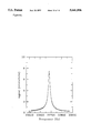
- FIGS. 8A, 8B and 8C show signal as a function of dither frequency for an embodiment in which a probe head comprising a tuning fork in accordance with FIG. 7B is used.
- the tuning fork is attached to a ceramic dither block 50 of the type described in conjunction with FIG. 4.
- An optical fiber 20 is attached to the tuning fork in the manner shown, for example, in FIG. 4.
- the signal measured is the amplitude of the AC voltage picked up from the contacts 40, 41, this signal being induced by the flexure of the prongs of the tuning fork as shown in FIGS. 5A, 5B, and 5C.
- the pick-up signal is measured as the dither frequency is varied.
- the measurement was made in air with the tip piece well away from any sample, i.e. in the absence of tip-sample interaction.
- the points are measured data and the lines fits calculated from a driven harmonic oscillator model.
- the resonance frequency is measured to be 33683 Hertz and the Q-factor 1410.
- the frequency resolution is 1.94 Hertz.
- a peak signal of approximately 7.5 microvolts is measured.
- FIG. 8B shows the effect of tip-sample interaction on the probe head response.
- the highest, sharpest peak corresponds to the situation shown in FIG. 8A, namely no tip-sample interaction.
- the response is then measured with progressively increasing interaction. From fight-to-left in the figure the tip-sample drag force or ⁇ friction ⁇ is measured at 0, 0.6, 1.2 and 3 nanonewtons, whereby the oscillations become increasingly damped.
- the points are measured data and the lines fits calculated from a driven harmonic oscillator model. Frequency resolution is 1.94 Hertz.
- the signal at the peak frequency for no interaction is a sensitive measure of the degree of tip-sample interaction.
- the frequency shift of the response peak with drag force is accompanied by a reduction in the Q-factor so that the signal at the peak frequency for no interaction remains measurable over a wide range of tip-sample drag force. Consequently, a simple, fixed frequency dither is still practical for an SPM in accordance with the invention.
- the signal is used to maintain a constant tip-sample distance. Distances in the range of 0 to 200 nanometers are usual.
- FIG. 8C shows the effect that bonding the tip piece onto the tuning fork has on the oscillator properties.
- the fight-hand peak shows the tuning fork response prior to bonding the tip piece onto the tuning fork.
- the measurement system was not accurate enough to measure the Q-factor of the true peak signal value because the resonance is too sharp. However, a lower limit of 5000 can be placed on the Q-factor, this probably being a considerable underestimate.
- the left-hand peak shows a similar response after bonding of the tip piece onto the same tuning fork, i.e. in an assembled probe head.
- the Q-factor has reduced to a value of 3560. Frequency resolution 1.94 Hertz.
- the standard way of regulating tip-sample distance in SPMs is to use the amplitude of the signal, whether it be a tunnel current (STM), atomic force (AFM) or some other convenient scalar quantity in a feed-back loop with a piezo translator which controls the tip-sample distance.
- STM tunnel current
- AFM atomic force
- Such a way of operating is also suitable for SPMs in accordance with the invention.
- the response of a tuning fork can be considered as electrically equivalent to a capacitance connected in series with a capacitance, inductance and resistance. Moreover, this impedance peaks at the resonance frequency of the tuning fork. Since tip-sample interaction affects the deformation of the tuning fork and induces detuning as shown for example in FIG. 8B, measurement of the impedance of the tuning fork is sensitive to the tip-sample interaction. It is thus possible to use the impedance to regulate the tip-sample distance. For instance, the tip-sample distance can be maintained at a distance defined by a constant impedance value.
- An SPM with a contact arrangement as shown in FIG. 7C can be dithered using an external drive circuit (not shown) by applying an AC dither drive input to the contacts 44, 45 with a frequency near to the resonance frequency of the tuning fork.
- the weak piezoelectric signal sensed by the pick-up electrodes 40, 41 is fed into a voltage amplifier 46 with adjustable gain and/or phase.
- the output of the amplifier is fed back to the contacts 44, 45 causing the fork to vibrate at its own inherent oscillation frequency.
- the tuning force is thus used as its own oscillator.
- the gain and phase of the amplifier are set so that the signal feeds itself in a closed loop.
- FIGS. 9A and 9B show images of blood cells taken with an SPM of the invention.
- the image size is approximately 13 by 13 micrometers.
- FIG. 9A is a topography image taken in FFM mode.
- FIG. 9B is an optical transmission image taken in NSOM mode. Both images 9A and 9B were taken simultaneously.
- FIG. 10 is an image of an optical grating formed on the surface of a piece of gallium arsenide single crystal taken in AFM mode.
- the areal image size is approximately 1 by 1 micrometers and the vertical scale, i.e. perpendicular to the gallium arsenide surface, has been expanded for clarity and amounts to only approximately 90 nanometers.
- FIGS. 6A and 6B show further embodiments of SPMs in accordance with the invention.
- the same reference numerals as in FIGS. 4, 7A, 7B and 7C are retained for analogous parts. Only some of the major pans are shown, since these figures are primarily intended to show the principles involved.
- FIG. 6A shows an embodiment incorporating an optical fiber 20 in the manner of FIG. 4 but using a twin-bimorph coupled oscillator arrangement.
- Each arm is a bimorph bar comprising a first strip 30a, 31a of one kind of piezoelectric material bonded together with a second strip 30b, 31b of another kind of piezoelectric material.
- the individual arms are connected by electrically conducting wires (dashed lines) which serve to couple the mechanical oscillations of the respective arms. Pick-up contacts are not shown to avoid cluttering up the figure.
- the dither block 50 is placed under the sample S and the part 60 holding the bimorphs together is a simple mounting block. In other words in this embodiment the relative movement between tip and sample is produced by vibrating the sample instead of the tip.
- Such an arrangement is particularly suited to a mode of use whereby, in the absence of tip-sample interaction, the arms 30, 31 remain still, whereas tip-sample interaction causes the arms to ting, i.e. to start oscillating. To do this the dither frequency should be matched to the natural oscillation frequency of the coupled oscillator arrangement.
- FIG. 6B shows an embodiment incorporating an optical fiber 20 bonded to the piezoelectric arm 30 in the manner of FIG. 4.
- the arm 30 is a single piece of piezoelectric material. This is the first oscillator 30.
- an electrical oscillator circuit 31 is provided.
- the two oscillators 30, 31 are connected by electrically conducting wires (dashed lines) which serve to couple the mechanical oscillations of the arm 30 and the electrical oscillations in the circuit 31.
- the pick-up contact geometry is not shown to avoid cluttering up the figure.
- a comparable embodiment could be made wherein the first oscillator is not a single piece of piezoelectric material but a bimorph.
- An electrical oscillator circuit 31 is used as the second oscillator.
Landscapes
- Physics & Mathematics (AREA)
- Health & Medical Sciences (AREA)
- General Health & Medical Sciences (AREA)
- General Physics & Mathematics (AREA)
- Nuclear Medicine, Radiotherapy & Molecular Imaging (AREA)
- Radiology & Medical Imaging (AREA)
- Chemical & Material Sciences (AREA)
- Nanotechnology (AREA)
- Engineering & Computer Science (AREA)
- Crystallography & Structural Chemistry (AREA)
- Optics & Photonics (AREA)
- Biophysics (AREA)
- Life Sciences & Earth Sciences (AREA)
- Analytical Chemistry (AREA)
- Length Measuring Devices With Unspecified Measuring Means (AREA)
- Length Measuring Devices By Optical Means (AREA)
Priority Applications (1)
| Application Number | Priority Date | Filing Date | Title |
|---|---|---|---|
| US08/827,216 US6006594A (en) | 1994-05-11 | 1997-03-28 | Scanning probe microscope head with signal processing circuit |
Applications Claiming Priority (2)
| Application Number | Priority Date | Filing Date | Title |
|---|---|---|---|
| GB9409414A GB2289759B (en) | 1994-05-11 | 1994-05-11 | Coupled oscillator scanning imager |
| GB9409414 | 1994-05-11 |
Related Child Applications (1)
| Application Number | Title | Priority Date | Filing Date |
|---|---|---|---|
| US08/827,216 Continuation-In-Part US6006594A (en) | 1994-05-11 | 1997-03-28 | Scanning probe microscope head with signal processing circuit |
Publications (1)
| Publication Number | Publication Date |
|---|---|
| US5641896A true US5641896A (en) | 1997-06-24 |
Family
ID=10754958
Family Applications (1)
| Application Number | Title | Priority Date | Filing Date |
|---|---|---|---|
| US08/395,089 Expired - Lifetime US5641896A (en) | 1994-05-11 | 1995-02-27 | Coupled oscillator scanning imager |
Country Status (4)
| Country | Link |
|---|---|
| US (1) | US5641896A (de) |
| CH (1) | CH686906A5 (de) |
| DE (1) | DE19510368C2 (de) |
| GB (1) | GB2289759B (de) |
Cited By (34)
| Publication number | Priority date | Publication date | Assignee | Title |
|---|---|---|---|---|
| EP0896201A1 (de) * | 1997-08-04 | 1999-02-10 | Seiko Instruments Inc. | Rastersondenmikroskop |
| US5939623A (en) * | 1996-02-20 | 1999-08-17 | Seiko Instruments Inc. | Scanning type near field interatomic force microscope |
| US5985085A (en) * | 1997-10-01 | 1999-11-16 | Arcturus Engineering, Inc. | Method of manufacturing consumable for laser capture microdissection |
| US5990477A (en) * | 1997-04-10 | 1999-11-23 | Seiko Instruments Inc. | Apparatus for machining, recording, and reproducing, using scanning probe microscope |
| US6006594A (en) * | 1994-05-11 | 1999-12-28 | Dr. Khaled Und Dr. Miles Haines Gesellschaft Burgerlichen Rechts | Scanning probe microscope head with signal processing circuit |
| US6094971A (en) * | 1997-09-24 | 2000-08-01 | Texas Instruments Incorporated | Scanning-probe microscope including non-optical means for detecting normal tip-sample interactions |
| WO2001006296A1 (en) * | 1999-07-20 | 2001-01-25 | Martin Moskovits | High q-factor micro tuning fork by thin optical fiber for nsom |
| US6184973B1 (en) | 1997-02-07 | 2001-02-06 | Arcturus Engineering, Inc. | Laser capture microdissection pressure plate and transfer arm |
| US6194711B1 (en) * | 1997-03-12 | 2001-02-27 | Seiko Instruments Inc. | Scanning near-field optical microscope |
| US6201227B1 (en) * | 1997-04-09 | 2001-03-13 | Seiko Instruments Inc. | Scanning probe microscope |
| US6223591B1 (en) * | 1997-11-28 | 2001-05-01 | Nikon Corporation | Probe needle arrangement and movement method for use in an atomic force microscope |
| US6234009B1 (en) * | 1998-05-04 | 2001-05-22 | International Business Machines Corporation | Controlling motion of a scanning force microscope probe tip moving into engagement with a sample surface |
| US6240771B1 (en) * | 1999-02-25 | 2001-06-05 | Franz J. Giessibl | Device for noncontact intermittent contact scanning of a surface and a process therefore |
| WO2001023939A3 (de) * | 1999-09-30 | 2001-08-16 | Surface Imaging Systems S I S | Vorrichtung zur optischen nahfeldmikroskopie |
| EP1055901A3 (de) * | 1999-05-24 | 2001-10-10 | Jasco Corporation | Rasterabtastmikroskop |
| US6373049B1 (en) * | 1999-05-03 | 2002-04-16 | Industrial Technology Research Institute | Knock mode scanning near-field optical microscope |
| US6495195B2 (en) | 1997-02-14 | 2002-12-17 | Arcturus Engineering, Inc. | Broadband absorbing film for laser capture microdissection |
| US20030086161A1 (en) * | 1997-07-16 | 2003-05-08 | Harris Martin Russell | Scanning microscope with miniature head |
| JP3481213B2 (ja) | 2001-03-22 | 2003-12-22 | 日本電子株式会社 | 原子間力顕微鏡における試料観察方法および原子間力顕微鏡 |
| RU2221287C2 (ru) * | 2002-03-14 | 2004-01-10 | Зао "Нт-Мдт" | Оптический зонд на основе кварцевого резонатора для сканирующего зондового микроскопа |
| US20040159781A1 (en) * | 2001-05-11 | 2004-08-19 | Terunobu Akiyama | Actuating and sensing device for scanning probe microscopes |
| US20040182140A1 (en) * | 2003-03-17 | 2004-09-23 | Weide Daniel Van Der | Heterodyne feedback system for scanning force microscopy and the like |
| DE10226801B4 (de) * | 2002-06-15 | 2005-03-31 | Bundesrepublik Deutschland, vertr. d. d. Bundesministerium für Wirtschaft und Arbeit, dieses vertr. d. d. Präsidenten der Physikalisch-Technischen Bundesanstalt | Oberflächenmessvorrichtung und Verfahren zur mechanischen sowie berührungslosen-optischen Untersuchung von Objektoberflächen |
| US20060148070A1 (en) * | 1997-10-01 | 2006-07-06 | Baer Thomas M | Consumable for laser capture microdissection |
| US7473401B1 (en) | 1997-12-04 | 2009-01-06 | Mds Analytical Technologies (Us) Inc. | Fluidic extraction of microdissected samples |
| US7584653B2 (en) | 2003-08-11 | 2009-09-08 | Veeco Instruments, Inc. | System for wide frequency dynamic nanomechanical analysis |
| JP2009541742A (ja) * | 2006-06-21 | 2009-11-26 | ユニバーシティ・オブ・デイトン | 偏光設計の方法およびそれらの適用例 |
| US20100154084A1 (en) * | 2007-04-24 | 2010-06-17 | The University Of Akron | Method and apparatus for performing apertureless near-field scanning optical microscopy |
| WO2012084994A1 (fr) | 2010-12-22 | 2012-06-28 | Commissariat à l'énergie atomique et aux énergies alternatives | Sonde de microscope à force atomique, son procédé de préparation et ses utilisations |
| CN103884418A (zh) * | 2014-04-17 | 2014-06-25 | 山西大学 | 基于声激励的音叉式石英晶振谐振频率的测量方法及装置 |
| CN105334157A (zh) * | 2015-10-23 | 2016-02-17 | 清华大学 | 滑动摩擦系数测量装置和滑动摩擦系数测量方法 |
| CN105467159A (zh) * | 2015-12-29 | 2016-04-06 | 中国科学院物理研究所 | 一种基于扫描探针技术的定位系统及其使用方法 |
| CN109883580A (zh) * | 2019-03-19 | 2019-06-14 | 西安交通大学 | 一种全石英差动式谐振压力传感器芯片 |
| CN112985251A (zh) * | 2021-03-24 | 2021-06-18 | 新乡学院 | 一种微观表面形貌测量装置及方法 |
Families Citing this family (10)
| Publication number | Priority date | Publication date | Assignee | Title |
|---|---|---|---|---|
| EP0864898A1 (de) * | 1997-03-12 | 1998-09-16 | Karrai-Haines GbR | Optisches Nahfeldmikroskop |
| EP0864846A3 (de) * | 1997-03-12 | 2000-12-13 | Haines, Miles, Dr. | Rasterabtastmikroskop |
| DE19713746C2 (de) * | 1997-04-03 | 2001-06-28 | Inst Mikrotechnik Mainz Gmbh | Sensor für gleichzeitige Rasterkraftmikroskopie und optische Nahfeldmikroskopie |
| AUPO790197A0 (en) * | 1997-07-16 | 1997-08-07 | Optiscan Pty Limited | Scanning microscope with miniature head |
| DE19852833A1 (de) * | 1998-11-17 | 2000-05-18 | Thomas Stifter | Verfahren zur Bestimmung des Abstandes einer Nahfeldsonde von einer zu untersuchenden Probenoberfläche und Nahfeldmikroskop |
| JP3819250B2 (ja) * | 2000-05-15 | 2006-09-06 | 株式会社ミツトヨ | 加振型接触検出センサ |
| GB2374201A (en) * | 2001-04-03 | 2002-10-09 | Khaled Karrai | Laser |
| DE112005002322B4 (de) * | 2004-09-24 | 2021-04-22 | Hoya Corp. | Abtasteinrichtung, optischer Kopf, optisches Instrument und Abtastverfahren |
| DE102012109580A1 (de) * | 2012-10-09 | 2014-04-10 | Prüftechnik Dieter Busch AG | Sensoranordnung und Verfahren zum Herstellen einer Sensoranordnung |
| CN115752203B (zh) * | 2022-11-23 | 2025-05-09 | 西安交通大学 | 基于摩擦纳米发电的真空开关位移传感器装置 |
Citations (11)
| Publication number | Priority date | Publication date | Assignee | Title |
|---|---|---|---|---|
| US4343993A (en) * | 1979-09-20 | 1982-08-10 | International Business Machines Corporation | Scanning tunneling microscope |
| EP0112401A1 (de) * | 1982-12-27 | 1984-07-04 | International Business Machines Corporation | Optisches Nahfeldabtastmikroskop |
| EP0394962A2 (de) * | 1989-04-24 | 1990-10-31 | Olympus Optical Co., Ltd. | Atomkraftmikroskop |
| EP0422548A2 (de) * | 1989-10-09 | 1991-04-17 | Olympus Optical Co., Ltd. | Atomkraftmikroskop |
| US5105305A (en) * | 1991-01-10 | 1992-04-14 | At&T Bell Laboratories | Near-field scanning optical microscope using a fluorescent probe |
| EP0487233A2 (de) * | 1990-11-19 | 1992-05-27 | AT&T Corp. | Optisches Nahfeldabtastmikroskop und dessen Anwendungen |
| US5212987A (en) * | 1988-06-16 | 1993-05-25 | Hommelwerke Gmbh | Acoustic screen scan microscope for the examination of an object in the short-range field of a resonant acoustic oscillator |
| EP0545538A1 (de) * | 1991-11-04 | 1993-06-09 | AT&T Corp. | Raster-Mikroskop mit einem Kraftfühler |
| US5280341A (en) * | 1992-02-27 | 1994-01-18 | International Business Machines Corporation | Feedback controlled differential fiber interferometer |
| EP0587459A1 (de) * | 1992-08-07 | 1994-03-16 | Digital Instruments, Inc. | Atomkraftmikroskop für ultrakleine Kräfte |
| US5467642A (en) * | 1992-11-06 | 1995-11-21 | Hitachi, Ltd. | Scanning probe microscope and method of control error correction |
Family Cites Families (3)
| Publication number | Priority date | Publication date | Assignee | Title |
|---|---|---|---|---|
| EP0290647B1 (de) * | 1987-05-12 | 1991-07-24 | International Business Machines Corporation | Atomares Kräftemikroskop mit oscillierendem Quarz |
| DE3820518C1 (de) * | 1988-06-16 | 1990-01-11 | Wild Leitz Gmbh, 6330 Wetzlar, De | |
| JPH03167744A (ja) * | 1989-11-27 | 1991-07-19 | Seiko Instr Inc | 微小距離移動機構 |
-
1994
- 1994-05-11 GB GB9409414A patent/GB2289759B/en not_active Expired - Lifetime
-
1995
- 1995-02-27 US US08/395,089 patent/US5641896A/en not_active Expired - Lifetime
- 1995-03-22 DE DE19510368A patent/DE19510368C2/de not_active Expired - Lifetime
- 1995-05-05 CH CH01332/95A patent/CH686906A5/de not_active IP Right Cessation
Patent Citations (11)
| Publication number | Priority date | Publication date | Assignee | Title |
|---|---|---|---|---|
| US4343993A (en) * | 1979-09-20 | 1982-08-10 | International Business Machines Corporation | Scanning tunneling microscope |
| EP0112401A1 (de) * | 1982-12-27 | 1984-07-04 | International Business Machines Corporation | Optisches Nahfeldabtastmikroskop |
| US5212987A (en) * | 1988-06-16 | 1993-05-25 | Hommelwerke Gmbh | Acoustic screen scan microscope for the examination of an object in the short-range field of a resonant acoustic oscillator |
| EP0394962A2 (de) * | 1989-04-24 | 1990-10-31 | Olympus Optical Co., Ltd. | Atomkraftmikroskop |
| EP0422548A2 (de) * | 1989-10-09 | 1991-04-17 | Olympus Optical Co., Ltd. | Atomkraftmikroskop |
| EP0487233A2 (de) * | 1990-11-19 | 1992-05-27 | AT&T Corp. | Optisches Nahfeldabtastmikroskop und dessen Anwendungen |
| US5105305A (en) * | 1991-01-10 | 1992-04-14 | At&T Bell Laboratories | Near-field scanning optical microscope using a fluorescent probe |
| EP0545538A1 (de) * | 1991-11-04 | 1993-06-09 | AT&T Corp. | Raster-Mikroskop mit einem Kraftfühler |
| US5280341A (en) * | 1992-02-27 | 1994-01-18 | International Business Machines Corporation | Feedback controlled differential fiber interferometer |
| EP0587459A1 (de) * | 1992-08-07 | 1994-03-16 | Digital Instruments, Inc. | Atomkraftmikroskop für ultrakleine Kräfte |
| US5467642A (en) * | 1992-11-06 | 1995-11-21 | Hitachi, Ltd. | Scanning probe microscope and method of control error correction |
Non-Patent Citations (28)
| Title |
|---|
| Akamine, S., et al., "Microfabricated Scanning Tunneling Microscope," IEEE Electron Device Letters, vol. 10, No. 11, pp. 490-492 (Nov. 1989). |
| Akamine, S., et al., Microfabricated Scanning Tunneling Microscope, IEEE Electron Device Letters , vol. 10, No. 11, pp. 490 492 (Nov. 1989). * |
| Betzig et al Applied Physics Letters, vol. 60, No. 20 pp. 2484 2486 (May 1992) (American Institute of Physics). * |
| Betzig et al Applied Physics Letters, vol. 60, No. 20 pp. 2484-2486 (May 1992) (American Institute of Physics). |
| Betzig, E., et al., "Breaking the Diffraction Barrier: Optical Microscopy on a Nanometric Scale," Science, vol. 251, pp. 1468-1470 (Mar. 22, 1991). |
| Betzig, E., et al., Breaking the Diffraction Barrier: Optical Microscopy on a Nanometric Scale, Science , vol. 251, pp. 1468 1470 (Mar. 22, 1991). * |
| Buckland, E.L., et al., "Resolution in Collection-Mode Scanning Optical Microscopy," Journal of Applied Physics, vol. 73, No. 3, pp. 1018-1028 (Feb. 1, 1993). |
| Buckland, E.L., et al., Resolution in Collection Mode Scanning Optical Microscopy, Journal of Applied Physics , vol. 73, No. 3, pp. 1018 1028 (Feb. 1, 1993). * |
| Clayton, L., et al., "Miniature Crystalline Quartz Electromechanical Structures," Sensors and Actuators, vol. 20, pp. 171-177 (1989). |
| Clayton, L., et al., Miniature Crystalline Quartz Electromechanical Structures, Sensors and Actuators , vol. 20, pp. 171 177 (1989). * |
| Grober, R., et al., "Design and Implementation of a Low Temperature Near-Field Scanning Optical Microscope," Review of Scientific Instruments, vol. 65, No. 3, pp. 626-631 (Mar. 1994). |
| Grober, R., et al., Design and Implementation of a Low Temperature Near Field Scanning Optical Microscope, Review of Scientific Instruments , vol. 65, No. 3, pp. 626 631 (Mar. 1994). * |
| Itoh, T., et al., "Piezoelectric Sensor for Detecting Force Gradients in Atomic Force Microscopy," Japanese Journal of Applied Physics, vol. 33, Pt. 1, No. 1A, pp. 334-340 (Jan. 1994). |
| Itoh, T., et al., Piezoelectric Sensor for Detecting Force Gradients in Atomic Force Microscopy, Japanese Journal of Applied Physics , vol. 33, Pt. 1, No. 1A, pp. 334 340 (Jan. 1994). * |
| Patent Abstracts of Japan, JP A 3 167744, E 1123, vol. 15, No. 408 (Oct. 17, 1991). * |
| Patent Abstracts of Japan, JP-A-3-167744, E-1123, vol. 15, No. 408 (Oct. 17, 1991). |
| Pohl, D.W., et al., "Optical Stethoscopy: Image Recording with Resolution λ/20," Applied Physics Letters, vol. 44, No. 7, pp. 651-653 (Apr. 1, 1984). |
| Pohl, D.W., et al., Optical Stethoscopy: Image Recording with Resolution /20, Applied Physics Letters , vol. 44, No. 7, pp. 651 653 (Apr. 1, 1984). * |
| Sasaki, A., et al., "Scanning Shearing-Stress Microscopy of Gold Thin Films," Japanese Journal of Applied Physics, vol. 33, Pt. 2, No. 4A, pp. L 547 -L 549 (Apr. 1994). |
| Sasaki, A., et al., Scanning Shearing Stress Microscopy of Gold Thin Films, Japanese Journal of Applied Physics , vol. 33, Pt. 2, No. 4A, pp. L 547 L 549 (Apr. 1994). * |
| Takata, K., "Whole Electronic Cantilever Control for Atomic Force Microscopy," Review of Scientific Instruments, vol. 64, No. 9, pp. 2598-2600 (Sep. 1993). |
| Takata, K., Whole Electronic Cantilever Control for Atomic Force Microscopy, Review of Scientific Instruments , vol. 64, No. 9, pp. 2598 2600 (Sep. 1993). * |
| Tansock and Williams Ultramicroscopy, vol. 42 44, pp. 1464 1469 (1992) (Elsevier Science Publishers). * |
| Tansock and Williams Ultramicroscopy, vol. 42-44, pp. 1464-1469 (1992) (Elsevier Science Publishers). |
| Toledo Crow et al Applied Physics Letters, vol. 60, No. 24 pp. 2957 2959 (1992) (American Institute of Physics). * |
| Toledo-Crow et al Applied Physics Letters, vol. 60, No. 24 pp. 2957-2959 92) (American Institute of Physics). |
| Tortonese et al Applied Physics Letters, vol. 62, No. 8 pp. 834 836 (Feb. 1993) (American Institute of Physics). * |
| Tortonese et al Applied Physics Letters, vol. 62, No. 8 pp. 834-836 (Feb. 1993) (American Institute of Physics). |
Cited By (57)
| Publication number | Priority date | Publication date | Assignee | Title |
|---|---|---|---|---|
| US6006594A (en) * | 1994-05-11 | 1999-12-28 | Dr. Khaled Und Dr. Miles Haines Gesellschaft Burgerlichen Rechts | Scanning probe microscope head with signal processing circuit |
| US5939623A (en) * | 1996-02-20 | 1999-08-17 | Seiko Instruments Inc. | Scanning type near field interatomic force microscope |
| US6700653B2 (en) | 1997-02-07 | 2004-03-02 | Arcturus Engineering, Inc. | Laser capture microdissection optical system |
| US6469779B2 (en) | 1997-02-07 | 2002-10-22 | Arcturus Engineering, Inc. | Laser capture microdissection method and apparatus |
| US6512576B1 (en) | 1997-02-07 | 2003-01-28 | Arcturus Engineering, Inc. | Laser capture microdissection optical system |
| US6639657B2 (en) | 1997-02-07 | 2003-10-28 | Arcturus Engineering, Inc. | Laser capture microdissection translation stage joystick |
| US7012676B2 (en) | 1997-02-07 | 2006-03-14 | Arcturus Bioscience, Inc. | Laser capture microdissection translation stage joystick |
| US6184973B1 (en) | 1997-02-07 | 2001-02-06 | Arcturus Engineering, Inc. | Laser capture microdissection pressure plate and transfer arm |
| US20040027556A1 (en) * | 1997-02-07 | 2004-02-12 | Baer Thomas M. | Laser capture microdissection translation stage joystick |
| US6697149B2 (en) | 1997-02-07 | 2004-02-24 | Arcturus Engineering, Inc. | Laser capture microdissection vacuum hold-down |
| US6215550B1 (en) * | 1997-02-07 | 2001-04-10 | Arcturus Engineering, Inc. | Laser capture microdissection optical system |
| US20040106206A1 (en) * | 1997-02-07 | 2004-06-03 | Baer Thomas M. | Laser capture microdissection vacuum hold-down |
| US6924889B2 (en) | 1997-02-07 | 2005-08-02 | Arcturus Bioscience, Inc. | Laser capture microdissection vacuum hold-down |
| US20030031781A1 (en) * | 1997-02-14 | 2003-02-13 | Baer Thomas M. | Broadband absorbing film for laser capture microdissection |
| US6495195B2 (en) | 1997-02-14 | 2002-12-17 | Arcturus Engineering, Inc. | Broadband absorbing film for laser capture microdissection |
| US6194711B1 (en) * | 1997-03-12 | 2001-02-27 | Seiko Instruments Inc. | Scanning near-field optical microscope |
| US6201227B1 (en) * | 1997-04-09 | 2001-03-13 | Seiko Instruments Inc. | Scanning probe microscope |
| US5990477A (en) * | 1997-04-10 | 1999-11-23 | Seiko Instruments Inc. | Apparatus for machining, recording, and reproducing, using scanning probe microscope |
| US6967772B2 (en) * | 1997-07-16 | 2005-11-22 | Optiscan Pty Ltd | Scanning microscope with miniature head |
| US20030086161A1 (en) * | 1997-07-16 | 2003-05-08 | Harris Martin Russell | Scanning microscope with miniature head |
| US6249000B1 (en) | 1997-08-04 | 2001-06-19 | Seiko Instruments Inc. | Scanning probe microscope |
| EP0896201A1 (de) * | 1997-08-04 | 1999-02-10 | Seiko Instruments Inc. | Rastersondenmikroskop |
| US6094971A (en) * | 1997-09-24 | 2000-08-01 | Texas Instruments Incorporated | Scanning-probe microscope including non-optical means for detecting normal tip-sample interactions |
| US7221447B2 (en) | 1997-10-01 | 2007-05-22 | Molecular Devices Corporation | Consumable for laser capture microdissection |
| US5985085A (en) * | 1997-10-01 | 1999-11-16 | Arcturus Engineering, Inc. | Method of manufacturing consumable for laser capture microdissection |
| US20060148070A1 (en) * | 1997-10-01 | 2006-07-06 | Baer Thomas M | Consumable for laser capture microdissection |
| US7075640B2 (en) | 1997-10-01 | 2006-07-11 | Arcturus Bioscience, Inc. | Consumable for laser capture microdissection |
| US6223591B1 (en) * | 1997-11-28 | 2001-05-01 | Nikon Corporation | Probe needle arrangement and movement method for use in an atomic force microscope |
| US7473401B1 (en) | 1997-12-04 | 2009-01-06 | Mds Analytical Technologies (Us) Inc. | Fluidic extraction of microdissected samples |
| US6234009B1 (en) * | 1998-05-04 | 2001-05-22 | International Business Machines Corporation | Controlling motion of a scanning force microscope probe tip moving into engagement with a sample surface |
| US6240771B1 (en) * | 1999-02-25 | 2001-06-05 | Franz J. Giessibl | Device for noncontact intermittent contact scanning of a surface and a process therefore |
| US6373049B1 (en) * | 1999-05-03 | 2002-04-16 | Industrial Technology Research Institute | Knock mode scanning near-field optical microscope |
| EP1055901A3 (de) * | 1999-05-24 | 2001-10-10 | Jasco Corporation | Rasterabtastmikroskop |
| US6470738B2 (en) * | 1999-05-24 | 2002-10-29 | Jasco Corporation | Rotating probe microscope |
| US6515274B1 (en) | 1999-07-20 | 2003-02-04 | Martin Moskovits | Near-field scanning optical microscope with a high Q-factor piezoelectric sensing element |
| WO2001006296A1 (en) * | 1999-07-20 | 2001-01-25 | Martin Moskovits | High q-factor micro tuning fork by thin optical fiber for nsom |
| WO2001023939A3 (de) * | 1999-09-30 | 2001-08-16 | Surface Imaging Systems S I S | Vorrichtung zur optischen nahfeldmikroskopie |
| JP3481213B2 (ja) | 2001-03-22 | 2003-12-22 | 日本電子株式会社 | 原子間力顕微鏡における試料観察方法および原子間力顕微鏡 |
| US20040159781A1 (en) * | 2001-05-11 | 2004-08-19 | Terunobu Akiyama | Actuating and sensing device for scanning probe microscopes |
| US7051582B2 (en) * | 2001-05-11 | 2006-05-30 | Institut De Microtechnique De L'universite De Neuchatel | Actuating and sensing device for scanning probe microscopes |
| RU2221287C2 (ru) * | 2002-03-14 | 2004-01-10 | Зао "Нт-Мдт" | Оптический зонд на основе кварцевого резонатора для сканирующего зондового микроскопа |
| DE10226801B4 (de) * | 2002-06-15 | 2005-03-31 | Bundesrepublik Deutschland, vertr. d. d. Bundesministerium für Wirtschaft und Arbeit, dieses vertr. d. d. Präsidenten der Physikalisch-Technischen Bundesanstalt | Oberflächenmessvorrichtung und Verfahren zur mechanischen sowie berührungslosen-optischen Untersuchung von Objektoberflächen |
| US6845655B2 (en) | 2003-03-17 | 2005-01-25 | Wisconsin Alumni Research Foundation | Heterodyne feedback system for scanning force microscopy and the like |
| US20040182140A1 (en) * | 2003-03-17 | 2004-09-23 | Weide Daniel Van Der | Heterodyne feedback system for scanning force microscopy and the like |
| US7584653B2 (en) | 2003-08-11 | 2009-09-08 | Veeco Instruments, Inc. | System for wide frequency dynamic nanomechanical analysis |
| US8248599B2 (en) * | 2006-06-21 | 2012-08-21 | University Of Dayton | Methods of polarization engineering and their applications |
| JP2009541742A (ja) * | 2006-06-21 | 2009-11-26 | ユニバーシティ・オブ・デイトン | 偏光設計の方法およびそれらの適用例 |
| US20100141939A1 (en) * | 2006-06-21 | 2010-06-10 | University Of Dayton | Methods of polarization engineering and their applications |
| US20100154084A1 (en) * | 2007-04-24 | 2010-06-17 | The University Of Akron | Method and apparatus for performing apertureless near-field scanning optical microscopy |
| WO2012084994A1 (fr) | 2010-12-22 | 2012-06-28 | Commissariat à l'énergie atomique et aux énergies alternatives | Sonde de microscope à force atomique, son procédé de préparation et ses utilisations |
| US8959661B2 (en) | 2010-12-22 | 2015-02-17 | Commissariat à l'énergie atomique et aux énergies alternatives | Atomic force microscope probe, method for preparing same, and uses thereof |
| CN103884418A (zh) * | 2014-04-17 | 2014-06-25 | 山西大学 | 基于声激励的音叉式石英晶振谐振频率的测量方法及装置 |
| CN103884418B (zh) * | 2014-04-17 | 2015-12-09 | 山西大学 | 基于声激励的音叉式石英晶振谐振频率的测量方法及装置 |
| CN105334157A (zh) * | 2015-10-23 | 2016-02-17 | 清华大学 | 滑动摩擦系数测量装置和滑动摩擦系数测量方法 |
| CN105467159A (zh) * | 2015-12-29 | 2016-04-06 | 中国科学院物理研究所 | 一种基于扫描探针技术的定位系统及其使用方法 |
| CN109883580A (zh) * | 2019-03-19 | 2019-06-14 | 西安交通大学 | 一种全石英差动式谐振压力传感器芯片 |
| CN112985251A (zh) * | 2021-03-24 | 2021-06-18 | 新乡学院 | 一种微观表面形貌测量装置及方法 |
Also Published As
| Publication number | Publication date |
|---|---|
| GB2289759A (en) | 1995-11-29 |
| DE19510368C2 (de) | 2003-04-10 |
| GB2289759B (en) | 1996-05-22 |
| GB9409414D0 (en) | 1994-06-29 |
| DE19510368A1 (de) | 1995-11-23 |
| CH686906A5 (de) | 1996-07-31 |
Similar Documents
| Publication | Publication Date | Title |
|---|---|---|
| US5641896A (en) | Coupled oscillator scanning imager | |
| US6006594A (en) | Scanning probe microscope head with signal processing circuit | |
| Karrai et al. | Piezo-electric tuning fork tip—sample distance control for near field optical microscopes | |
| US5319977A (en) | Near field acoustic ultrasonic microscope system and method | |
| US6201227B1 (en) | Scanning probe microscope | |
| Friedt et al. | Introduction to the quartz tuning fork | |
| US8448502B2 (en) | Band excitation method applicable to scanning probe microscopy | |
| US6094971A (en) | Scanning-probe microscope including non-optical means for detecting normal tip-sample interactions | |
| US4851671A (en) | Oscillating quartz atomic force microscope | |
| Qin et al. | Calibrating a tuning fork for use as a scanning probe microscope force sensor | |
| US7979916B2 (en) | Preamplifying cantilever and applications thereof | |
| Akiyama et al. | Symmetrically arranged quartz tuning fork with soft cantilever for intermittent contact mode atomic force microscopy | |
| US20080092659A1 (en) | Whispering gallery mode ultrasonically coupled scanning probe microscopy | |
| US8387161B2 (en) | Scanning probe microscope | |
| US20100205698A1 (en) | Atomic force microscopy probe | |
| Akiyama et al. | Implementation and characterization of a quartz tuning fork based probe consisted of discrete resonators for dynamic mode atomic force microscopy | |
| US5886532A (en) | Nanometer distance regulation using electromechanical power dissipation | |
| KR100501893B1 (ko) | 주파수 응답 분리 방식을 이용한 비접촉식 측정 장치 및그 측정 방법 | |
| Shelimov et al. | Dynamics of a piezoelectric tuning fork/optical fiber assembly in a near-field scanning optical microscope | |
| Harley et al. | A high-stiffness axial resonant probe for atomic force microscopy | |
| JPH0989911A (ja) | 連成オシレータ走査イメージャー | |
| Mühlschlegel et al. | Glue-free tuning fork shear-force microscope | |
| Lei et al. | Shear force detection by using bimorph cantilever with the enhanced Q factor | |
| Decca et al. | Mechanical oscillator tip-to-sample separation control for near-field optical microscopy | |
| US10302673B2 (en) | Miniaturized and compact probe for atomic force microscopy |
Legal Events
| Date | Code | Title | Description |
|---|---|---|---|
| AS | Assignment |
Owner name: DR. KHALED KARRAI UND DR. MILES HAINES GESELLSCHA Free format text: ASSIGNMENT OF ASSIGNORS INTEREST;ASSIGNOR:KARRAI, KHALED;REEL/FRAME:007948/0141 Effective date: 19960506 |
|
| STCF | Information on status: patent grant |
Free format text: PATENTED CASE |
|
| FPAY | Fee payment |
Year of fee payment: 4 |
|
| AS | Assignment |
Owner name: KARRAI, KHALED, GERMANY Free format text: ASSIGNMENT OF ASSIGNORS INTEREST;ASSIGNOR:HAINES, MILES;REEL/FRAME:014027/0977 Effective date: 20021203 |
|
| FPAY | Fee payment |
Year of fee payment: 8 |
|
| SULP | Surcharge for late payment |
Year of fee payment: 7 |
|
| REMI | Maintenance fee reminder mailed | ||
| AS | Assignment |
Owner name: ATTOCUBE SYSTEMS AG, GERMAN DEMOCRATIC REPUBLIC Free format text: ASSIGNMENT OF ASSIGNORS INTEREST;ASSIGNOR:KARRAI, KHALED, MR.;REEL/FRAME:020119/0548 Effective date: 20071102 |
|
| FPAY | Fee payment |
Year of fee payment: 12 |
|
| REMI | Maintenance fee reminder mailed | ||
| SULP | Surcharge for late payment |