US5717519A - Confocal microscope - Google Patents
Confocal microscope Download PDFInfo
- Publication number
- US5717519A US5717519A US08/675,133 US67513396A US5717519A US 5717519 A US5717519 A US 5717519A US 67513396 A US67513396 A US 67513396A US 5717519 A US5717519 A US 5717519A
- Authority
- US
- United States
- Prior art keywords
- light
- lense
- microlenses
- incident
- objective
- Prior art date
- Legal status (The legal status is an assumption and is not a legal conclusion. Google has not performed a legal analysis and makes no representation as to the accuracy of the status listed.)
- Expired - Lifetime
Links
Images




Classifications
-
- G—PHYSICS
- G02—OPTICS
- G02B—OPTICAL ELEMENTS, SYSTEMS OR APPARATUS
- G02B21/00—Microscopes
- G02B21/0004—Microscopes specially adapted for specific applications
- G02B21/002—Scanning microscopes
- G02B21/0024—Confocal scanning microscopes (CSOMs) or confocal "macroscopes"; Accessories which are not restricted to use with CSOMs, e.g. sample holders
-
- G—PHYSICS
- G02—OPTICS
- G02B—OPTICAL ELEMENTS, SYSTEMS OR APPARATUS
- G02B21/00—Microscopes
- G02B21/0004—Microscopes specially adapted for specific applications
- G02B21/002—Scanning microscopes
- G02B21/0024—Confocal scanning microscopes (CSOMs) or confocal "macroscopes"; Accessories which are not restricted to use with CSOMs, e.g. sample holders
- G02B21/0028—Confocal scanning microscopes (CSOMs) or confocal "macroscopes"; Accessories which are not restricted to use with CSOMs, e.g. sample holders specially adapted for specific applications, e.g. for endoscopes, ophthalmoscopes, attachments to conventional microscopes
-
- G—PHYSICS
- G02—OPTICS
- G02B—OPTICAL ELEMENTS, SYSTEMS OR APPARATUS
- G02B21/00—Microscopes
- G02B21/0004—Microscopes specially adapted for specific applications
- G02B21/002—Scanning microscopes
- G02B21/0024—Confocal scanning microscopes (CSOMs) or confocal "macroscopes"; Accessories which are not restricted to use with CSOMs, e.g. sample holders
- G02B21/0032—Optical details of illumination, e.g. light-sources, pinholes, beam splitters, slits, fibers
-
- G—PHYSICS
- G02—OPTICS
- G02B—OPTICAL ELEMENTS, SYSTEMS OR APPARATUS
- G02B21/00—Microscopes
- G02B21/0004—Microscopes specially adapted for specific applications
- G02B21/002—Scanning microscopes
- G02B21/0024—Confocal scanning microscopes (CSOMs) or confocal "macroscopes"; Accessories which are not restricted to use with CSOMs, e.g. sample holders
- G02B21/0036—Scanning details, e.g. scanning stages
- G02B21/0044—Scanning details, e.g. scanning stages moving apertures, e.g. Nipkow disks, rotating lens arrays
-
- G—PHYSICS
- G02—OPTICS
- G02B—OPTICAL ELEMENTS, SYSTEMS OR APPARATUS
- G02B21/00—Microscopes
- G02B21/0004—Microscopes specially adapted for specific applications
- G02B21/002—Scanning microscopes
- G02B21/0024—Confocal scanning microscopes (CSOMs) or confocal "macroscopes"; Accessories which are not restricted to use with CSOMs, e.g. sample holders
- G02B21/0052—Optical details of the image generation
- G02B21/006—Optical details of the image generation focusing arrangements; selection of the plane to be imaged
Definitions
- This invention relates to confocal microscopes incorporating a confocal laser scanner which rotates a Nipkow disk at high speed together with a plurality of microlenses; and more particularly, to improvements of such confocal microscopes resulting in increased light use efficiency.
- Confocal microscopes are well known, as are confocal light scanners using Nipkow disks which are rotated at high speeds which light scanners are used in such microscopes.
- the conventional confocal microscopes using such confocal light scanners have problems involving inefficient use of light.
- FIG. 1 shows an example of a conventional confocal light scanner wherein a laser 1 transmits a light through microlenses (not shown) arranged in microlense disk 2 and cube shaped dichroic mirror 4, respectively, and the light is focused on pin holes (minute openings, not shown) formed in an array in Nipkow disk 3.
- the microlense disk may comprise the collector disk, for example, described in Japan Patent Appl. SN 1992/15,411 (Published 1993/60,980).
- collector disk 20 is formed of glass plate 21 on which a number of Fresnel lenses 22 are formed. The Fresnel lenses are so formed that the focusing position of each shifts radially, in turn, from one image plane to another image plane.
- Dichroic mirror 4 (see FIG. 1) is disposed in the space between microlense disk 2 and Nipkow disk 3 with a supporting mechanism not shown in FIG. 1. Light focused on the pin holes of Nipkow disk 3 is transmitted through objective lense 6 and is irradiated onto sample 7. Fluorescence emitted from sample 7 is focused onto the pin holes of disk 3 through objective lense 6. Thus, a real image of sample 7 is obtained at the pin holes. This image is reflected by dichroic mirror 4 and is formed on the light receiving plane of camera 9 through relay lense 8.
- Nipkow disk 3 is coupled to microlense disk 2 and both disks are rotated concurrently by motor 5. In such a configuration, a two dimensional image of the surface of sample 7 can be obtained on the light receiving plane of camera 9 by scanning the surface of sample 7 with a light beam by rotating microlense disk 2 and Nipkow disk 3.
- cube dichroic mirror 4 has a problem in that since it is formed of glass both in the front and back of the film and the refractive indices are the same, it is difficult to obtain a sharp characteristic for separating fluorescence from exciting light, as compared, for example, with a plate dichroic mirror which can provide a large difference between refractive indices on both sides because one side can be of air.
- Another object is to provide a confocal microscope which has improved light use efficiency.
- the invention encompasses a confocal microscope which employes a confocal light scanner and a plate beam splitter and wherein a converging laser beam is made to be incident on both the microlense and pinholes.
- the invention comprises a confocal light scanner provided with two integrated disks, in one of which a plurality of microlenses are arranged while in the other a plurality of minute openings are arranged, both being in an array of the same pattern, a rotation means for rotating the two disks, a beam splitter disposed between the two disks, and an objective lense disposed between the two disks and a sample, wherein a plate beam splitter is used as the beam splitter; the optical axis of light incident to the microlenses is tilted to the optical axis of a light vertical to the microlenses, and light incident to the microlenses is focused on the minute openings whose positions correspond to the relevant microlenses.
- a beam splitter such as a plate beam splitter, is disposed between the two disks, and the tilting of the optical axis cancels the shift of the optical axis caused by the plate beam splitter and causes the incident light to the microlense to be focused onto the corresponding minute openings.
- FIG. 1 is a diagram depicting a conventional confocal microscope.
- FIG. 2 is a diagram depicting a configuration of conventional microlenses.
- FIG. 3 is a diagram depicting shift of optical axis in a dichroic mirror.
- FIG. 4 is a diagram depicting a first illustrative embodiment of the invention as embodied in a confocal light scanner.
- FIG. 5 is an enlarged view depicting a dichroic mirror.
- FIG. 6 is a diagram depicting a second illustrative embodiment of the invention as embodied in a confocal light scanner.
- FIGS. 7, 8,9 and 10 are diagrams depicting, respectively, third, fourth, fifth and sixth illustrative embodiments of the invention as embodied in a confocal light scanner.
- FIG. 11 is a diagram depicting another exemplary conventional confocal microscope.
- FIG. 12 is a diagram depicting the relationship between the aperture of the objective lense and the laser light incident position shown in FIG. 11.
- FIG. 13 is a diagram depicting a first illustrative embodiment of a confocal microscope of the invention.
- FIG. 14 is a diagram depicting the relationship between the aperture of the objective lense and the laser light incident position in FIG. 13.
- FIG. 15 is a diagram depicting a conventional light scanner mounted on a microscope having a finite optical system.
- FIG. 16 is a diagram depicting the relationship between the aperture of the objective lense and the laser light incident position in FIG. 15.
- FIG. 17 is a diagram depicting a second illustrative embodiment of a confocal microscope of the invention.
- FIG. 18 is a diagram depicting the relationship between the aperture of the objective lense and the laser light incident position in FIG. 17.
- FIG. 19 is a diagram depicting a third illustrative embodiment of a confocal microscope of the invention.
- FIG. 1 the same symbols and numerals used in FIG. 1 represent the same parts in the remaining figures, and description of such parts is omitted hereafter for sake of brevity.
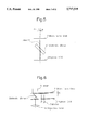
- a plate dichroic mirror 41 is positioned between microlense disk 2 and Nipkow disk 3.
- Laser 1 is positioned so that the light produced thereby is made to be incident on microlense disk 2 with an optical axis tilted by angle ⁇ from the vertical incident axis Z of microlenses in disk 2.
- the tilted angle ⁇ is determined in relation to the distance between microlense disk 2 and Nipkow disk 3 and the thickness of dichroic mirror 41.
- the laser light diaphragmed by the microlenses is shifted by its optical axis by dichroic mirror 41, then transmitted through the pin holes of Nipkow disk 3 and adjusted to be vertical under the microlense disk in the same pattern, and then scanned over a sample by being rotated by motor 5.
- the optical axis shift due to action of the plate dichroic mirror 41 can be corrected by having the laser light to be incident to microlense disk 2 with the laser light being tilted from the vertical.
- FIG. 6 shows the optical axis of the laser light to be tilted from the vertical incident axis to the microlenses.
- a unit in which microlense disk 2, Nipkow disk 3, dichroic mirror 41, and motor 5 are integrated is tilted by angle ⁇ from laser 1 with the optical axis of original laser 1 aligned with the vertical incident optical axis of the objective lense 6.
- the invention can be used with fluorescent confocal light scanners as well as with reflection confocal light scanners which use beam splitters, or half-mirrors, or polarized beam splitters, or the like, instead of dichroic mirrors.
- the invention can cancel the shift of the laser light optical axis due to the plate dichroic mirror 41 by tilting the optical axis by a significant angle against disk 2 and facilitate the use of the plate dichroic mirror having a characteristic of good fluroscent light separation from the exciting light.
- Increase of light use efficiency can also be accomplished by widening the field of view of the confocal microscope, such as shown in FIG. 1.
- microlenses of long focal lengths and a smaller number of apertures called "NA"
- NA apertures
- Such a configuration has the following problems.
- the following embodiment has the optical axis disposed on the peripheral side and light is returned to the pin holes with another mirror.
- the length of light path is extended by a relay lense. This enables use of a microlense of a short focal length and use of a commercially available dichroic mirror as the beam splitter.
- FIG. 7 shows the first (M 1 ), second (M 2 ), and third (M 3 ) reflection mirrors, respectively, and first (L 1 ) and second (L 2 ) relay lenses.
- Light transmitted through microlense ML in converging disk 2 is reflected with the first mirror M 1 diaphragmed with first lens L 1 and is made incident on beam splitter 12 (a dichroic mirror in this case).
- the incident light has shorter wavelengths, is reflected with dichroic mirror 12, then reflected with mirror M 2 , diaphragmed with second lense L 2 , reflected with third mirror M 3 and focused on pin hole PH in disk 3.
- the light focused on pin hole PH is transmitted through objective lense 6 and irradiates sample 7 is a way similar to that in the art.
- the return light from the sample is transmitted through objective lense 6 and forms an image of the sample on pin hole PH.
- the real image is reflected with third mirror M 3 , diaphragmed with second lense L 2 , reflected with second mirror M 2 , transmitted through beam splitter 12, and then diaphragmed with converging lense 43, and then focused on the light receiving plane of camera 9.
- mirrors M 1 , M 2 , M 3 , lenses L 1 , L 2 , beam splitter 12, converging lense 43 and camera 9 are arranged in fixed positions.
- the lengths of each light path from each microlense ML to its corresponding pin hole PH are the same. Since the light path is extended using relay lenses L 1 and L 2 so that the optical axis is introduced to the peripheral side of disks 14,15 with reflection mirror M 1 , and is returned to pin hole PH with second and third reflection mirrors M 2 and M 3 , microlenses ML of a short focal length can be used.
- beam splitter 12 reflects the incident light and transmits the return light
- a dichroic mirror of the type that reflects the incident light and transmits the return light can be used instead of beam splitter 12.
- a microlense of a short focal length for optical fibers available on the market can be used as the microlense ML. The adoption of such a construction makes the use of the microlenses of a short focal length and large NA's possible and enables the NA's of microlenses and the NA incident to pin holes to be designed separately.
- FIG. 8 differs from FIG. 7 in that a second lense L 2 is located between third mirror M 3 and pin hole disk 3 so that the system can cope with a large NA objective lense.
- the number of apertures of the objective lense is normally 0.2 for a magnification of 10 in a usual confocal microscope.
- the pin hole diameter is 30 ⁇ m.
- the case of large NA's i.e. a magnification of 10 and an objective lense NA of 0.9, produces the NA's at the pin hole of 0.09 and the pin hole diameter of 7 ⁇ m.
- small pin holes and large NA microlenses can be used together with large NA objective lenses.
- FIG. 9 differs from FIG. 7 in that there are only two mirrors M 1 and M 3 and second mirror M 2 is omitted.
- FIG. 10 differs from FIG. 7 in that lense L 2 and mirror M 2 are omitted.
- FIGS. 8,9, and 10 operate in a manner similar to the embodiment of FIG. 7.
- the placement of the mirrors and lenses between the microlenses and the pin holes enables the NA's of the microlenses on the light source side and the NA's on the pin hole side to be designed independently.
- the small pin holes and the microlenses of a short focal length and with large NA's can be used thereby facilitating the implementation of a measuring system having a wide field of view and large NA's.
- a reflection excitation dichroic mirror can be used instead of a beam splitter and hence a confocal microscope having a suitable wave length characteristic and of low cost can be realized.
- a plate dichroic mirror can be used.
- FIG. 11 Another embodiment for improving light use efficiency at the periphery of the field of view and for improving resolution, especially in a microscope comprising an infinite optical system is shown in FIG. 11, wherein an optical scanner 10 is attached to such a microscope and comprises a tube lense 20 and an objective lense 30.
- the laser light converged by microlense ML, in the optical scanner becomes a point source at the pin hole (i.e. the point sources from three pin holes are shown in the drawing) and the light beams from these points sources become parallel with each other via tube lense 20 and are made incident to objective lense 30.
- the interval between "b" between tube lense 20 and objective lense 30 is not equal to the focal length "a" of tube lense 20. Accordingly, if a confocal optical scanner with pin holes is attached to such a microscope having an infinite optical system, the light from the outside of the pin hole array is made incident to positions shifted from the center of the aperture of the objective lense 30 as shown in FIG. 12.
- Such a configuration has the following problems. First, the diameter of the aperture is small depending on the kind of objective lense 30. This reduces the amount of light from outside the pin holes.
- FIG. 13 differs from FIG. 11 in that spacer 50 is disposed between tube lense 20 and objective lense 30 so that the distance "b" between tube lense 20 and objective lense 30 is equal to the focal length "a" of tube lense 20.
- Spacer 20 is a hollow ring engaged with a cylinder, not shown, to which tube lense 20 and objective lense 30 are mounted, and acts to extend the cylinder. If such spacer 50 is mounted to equalize the distance "b" between tube lense 20 and objective lense 30 to the focal length "a" of tube lense 20, the laser light from all pin holes PH is made incident to the center of the aperture of objective lense 20 as a result, as shown in FIG. 14.
- the optical system can be operated without microlenses ML.
- the laser light from the pin holes at the outside areas can be made incident at the center of the aperture of the objective lense, the following effects are attained.
- the light use efficiency is increased and no illumination non-uniformity is generated.
- Second, both pin holes at the outer part and at the center part of the image area can equally and effectively use the aperture of the objective lense. The number of apertures is not decreased. Lowering of the resolution for the outer part does not occur.
- the above embodiments are for microscopes of an infinite optical system.
- the embodiment of FIG. 15 may be used.
- the distance of pin hole PH and objective lense 30 is equal to the image focal length "a" as shown in FIG. 15.
- all light beams from pin holes PH are made incident on objective lense 30 with the optical axis thereof being at 0 degrees and in parallel with each other, and the light from the outer part is made incident to the shifted part from the center of aperture of objective lense 30.
- a lense having the same focal length as the image focal of the objective lense is provided between the minute openings and the objective lens to enable the light from all minute openings to be incident to the center of the aperture of the objective lense, the loss of light at the outer part can be eliminated and light use efficiency can be improved. Also, the resolution at the outer part is raised.
- FIG. 17 shows an embodiment which differs from FIG. 15 in that field lense 60 is provided immediately under the pin hole array.
- Field lense 60 has the same focal length as the image focal length "a" of the objective lense 30 in a finite optical system microscope and is placed close to pin hole array 11.
- the laser light is diaphragmed by microlense ML into pin hole PH and the optical axis of the laser light that passes through pin hole PH is deflected toward the center of the objective lense 30 aperture by field lens 60 place immediately under pin hole PH. Accordingly, the laser light from all pin holes PH is made incident to the center of the aperture of objective lense 30, as shown in FIG. 18.
- the optical axis of the return light from the sample (not shown) is deflected by field lense 60 so that the optical axis is made incident at 0 degree to pin hole PH. This increases the light use efficiency. In this case, if field lense 60 is considerably distance from the pin hole surface, an aberration occurs. However, generally, since the focal length "a" can be designed to be about 200 mm, and the distance between pin hole PH and field lense 60 is designed to be about 10 mm, there is virtually no problem from aberration.
- FIG. 19 shows a relay lense 71 and a lense 72 disposed between pin hole PH and objective lense 30.
- Relay lense 71 forms an image plane of pin holes PH in the position of the image focal length "a" of objective lense 30 and is placed between pin holes PH and objective lense 30.
- Lense 72 has the same focal length as the image focal length "a” of objective lense 30 and is placed in the position of the image plane of pin hole PH obtained by relay lense 71. This configuration enables all of the light from the pin holes to be made incident to the center of the aperture of objective lense 30.
- microlense ML may be omitted.
- shape of the minute openings is not limited to a circle, but other suitable shapes may be used.
- the word “diaphragmed” or the like was used in connection with light being passed through a lense or microlense.
- the word “focused” can also be used in its place.
Landscapes
- Physics & Mathematics (AREA)
- Chemical & Material Sciences (AREA)
- Analytical Chemistry (AREA)
- General Physics & Mathematics (AREA)
- Optics & Photonics (AREA)
- Health & Medical Sciences (AREA)
- General Health & Medical Sciences (AREA)
- Ophthalmology & Optometry (AREA)
- Radiology & Medical Imaging (AREA)
- Surgery (AREA)
- Microscoopes, Condenser (AREA)
Priority Applications (1)
| Application Number | Priority Date | Filing Date | Title |
|---|---|---|---|
| US08/892,380 US5847867A (en) | 1996-07-03 | 1997-07-14 | Confocal microscope |
Applications Claiming Priority (8)
| Application Number | Priority Date | Filing Date | Title |
|---|---|---|---|
| JP17710495A JP3015912B2 (ja) | 1995-07-13 | 1995-07-13 | 共焦点光スキャナ |
| JP7-177104 | 1995-07-13 | ||
| JP21895995A JP2919776B2 (ja) | 1995-08-28 | 1995-08-28 | 共焦点顕微鏡 |
| JP7-218959 | 1995-08-28 | ||
| JP7-234938 | 1995-09-13 | ||
| JP07234938A JP3082183B2 (ja) | 1995-09-13 | 1995-09-13 | 共焦点顕微鏡 |
| JP7-329060 | 1995-12-18 | ||
| JP32906095A JP3189944B2 (ja) | 1995-12-18 | 1995-12-18 | 共焦点用光スキャナ |
Related Child Applications (1)
| Application Number | Title | Priority Date | Filing Date |
|---|---|---|---|
| US08/892,380 Division US5847867A (en) | 1996-07-03 | 1997-07-14 | Confocal microscope |
Publications (1)
| Publication Number | Publication Date |
|---|---|
| US5717519A true US5717519A (en) | 1998-02-10 |
Family
ID=27474749
Family Applications (1)
| Application Number | Title | Priority Date | Filing Date |
|---|---|---|---|
| US08/675,133 Expired - Lifetime US5717519A (en) | 1995-07-13 | 1996-07-03 | Confocal microscope |
Country Status (3)
| Country | Link |
|---|---|
| US (1) | US5717519A (fr) |
| EP (3) | EP1538470A3 (fr) |
| DE (3) | DE69629877T2 (fr) |
Cited By (23)
| Publication number | Priority date | Publication date | Assignee | Title |
|---|---|---|---|---|
| US5969846A (en) * | 1996-11-28 | 1999-10-19 | Olympus Optical Co., Ltd. | Confocal microscope |
| US6631029B2 (en) * | 2000-06-23 | 2003-10-07 | Yokogawa Electric Corporation | Optical image separation system and confocal scanning unit |
| US20040224421A1 (en) * | 2000-06-15 | 2004-11-11 | Deweerd Herman | Bi-directional scanning method |
| US20050007641A1 (en) * | 2001-04-10 | 2005-01-13 | Vincent Lauer | Modifiable assembly of microscopic apertures |
| US20050094261A1 (en) * | 2002-05-03 | 2005-05-05 | Stefan Hell | Confocal microscope comprising two microlens arrays and a pinhole diaphragm array |
| US7088650B1 (en) * | 1999-08-23 | 2006-08-08 | Worthington Mark O | Methods and apparatus for optical disc data acquisition using physical synchronization markers |
| US20090208370A1 (en) * | 2008-02-14 | 2009-08-20 | Yokogawa Electric Corporation | Drug discovery screening device |
| US20090279159A1 (en) * | 2007-02-27 | 2009-11-12 | Till I.D. Gmbh | Device for confocal illumination of a specimen |
| US20100117108A1 (en) * | 2006-09-28 | 2010-05-13 | X-Fab Semiconductor Foundries Ag | Uses of self-organized needle-type nanostructures |
| US20100142041A1 (en) * | 2008-12-09 | 2010-06-10 | Spectral Applied Research Inc. | Multi-Mode Fiber Optically Coupling a Radiation Source Module to a Multi-Focal Confocal Microscope |
| US20110134519A1 (en) * | 2009-12-08 | 2011-06-09 | Spectral Applied Research Inc. | Imaging Distal End of Multimode Fiber |
| US20110216404A1 (en) * | 2010-03-02 | 2011-09-08 | Yokogawa Electric Corporation | Confocal microscope system |
| US20110222051A1 (en) * | 2010-03-15 | 2011-09-15 | Bio-Rad Laboratories, Inc. | Microassembled imaging flow cytometer |
| WO2013086350A1 (fr) * | 2011-12-07 | 2013-06-13 | Celloptic, Inc. | Appareil permettant de produire un hologramme |
| US20150085360A1 (en) * | 2013-09-25 | 2015-03-26 | Canon Kabushiki Kaisha | Confocal microscope |
| US9122061B2 (en) | 2011-12-07 | 2015-09-01 | Yokogawa Electric Corporation | Confocal optical scanner and confocal microscope |
| DE102015011552A1 (de) | 2015-09-02 | 2017-03-02 | Visitron Systems GmbH | Verfahren und Anordnung zur Lichteinkopplung in ein Multifokales Konfokalmikroskop |
| US9606343B2 (en) | 2011-05-06 | 2017-03-28 | Visitech International Ltd | Enhancing spatial resolution utilizing multibeam confocal scanning systems |
| US20170276608A1 (en) * | 2014-04-24 | 2017-09-28 | Bruker Nano, Inc. | Super resolution microscopy |
| US20170336611A1 (en) * | 2016-05-23 | 2017-11-23 | Olympus Corporation | Microscope apparatus and specimen observation method |
| WO2018104536A1 (fr) | 2016-12-09 | 2018-06-14 | Leica Microsystems Cms Gmbh | Dispositif d'éclairage pour un microscope confocal et microscope confocal |
| US10520713B2 (en) | 2015-08-06 | 2019-12-31 | Till I.D. Gmbh | System for confocal illumination of a sample |
| US20230324664A1 (en) * | 2022-04-07 | 2023-10-12 | Till I.D. Gmbh | Spinning disk microscope device with potentially enhanced image resolution |
Families Citing this family (6)
| Publication number | Priority date | Publication date | Assignee | Title |
|---|---|---|---|---|
| DE19707226A1 (de) * | 1997-02-24 | 1998-08-27 | Bodenseewerk Perkin Elmer Co | Lichtabtastvorrichtung |
| DE10039520A1 (de) | 2000-08-08 | 2002-02-21 | Leica Microsystems | Vorrichtung zur Untersuchung und Manipulation von mikroskopischen Objekten |
| DE10044308A1 (de) * | 2000-09-07 | 2002-03-21 | Leica Microsystems | Verfahren und Vorrichtung zur Detektion von Fluoreszenzlicht bei der konfokalen Rastermikroskopie |
| JP3741051B2 (ja) * | 2001-05-10 | 2006-02-01 | 横河電機株式会社 | バイオチップ読取装置 |
| US20150131148A1 (en) | 2013-11-12 | 2015-05-14 | Intelligent Imaging Innovations, Inc. | Spinning disk confocal using paired microlens disks |
| EP3752879A1 (fr) | 2018-02-12 | 2020-12-23 | Intelligent Imaging Innovations, Inc. | Microscopie à feuille de lumiere (spim) à pavage utilisant des feuilles de lumiere discontinues |
Citations (3)
| Publication number | Priority date | Publication date | Assignee | Title |
|---|---|---|---|---|
| US5162941A (en) * | 1991-07-23 | 1992-11-10 | The Board Of Governors Of Wayne State University | Confocal microscope |
| US5351152A (en) * | 1991-07-23 | 1994-09-27 | The Board Of Governers Of Wayne State University | Direct-view stereoscopic confocal microscope |
| US5428475A (en) * | 1991-10-31 | 1995-06-27 | Yokogawa Electric Corporation | Confocal optical scanner |
Family Cites Families (7)
| Publication number | Priority date | Publication date | Assignee | Title |
|---|---|---|---|---|
| US5022743A (en) * | 1987-03-27 | 1991-06-11 | The Board Of Trustees Of The Leland Stanford Junior University | Scanning confocal optical microscope |
| US5067805A (en) * | 1990-02-27 | 1991-11-26 | Prometrix Corporation | Confocal scanning optical microscope |
| DE4023292A1 (de) * | 1990-07-21 | 1992-01-23 | Leica Lasertechnik | Anordnung zur simultanen konfokalen bilderzeugung |
| DE4023650A1 (de) * | 1990-07-25 | 1992-01-30 | Max Planck Gesellschaft | Ueberaufloesendes konfokales mikroskop |
| US5386317A (en) * | 1992-05-13 | 1995-01-31 | Prometrix Corporation | Method and apparatus for imaging dense linewidth features using an optical microscope |
| KR950704670A (ko) * | 1993-09-30 | 1995-11-20 | 가따다 데쯔야 | 공초점광학장치 |
| GB2289345B (en) * | 1994-05-06 | 1998-02-18 | Secretary Trade Ind Brit | Array of microlenses each associated with two pinholes |
-
1996
- 1996-07-03 US US08/675,133 patent/US5717519A/en not_active Expired - Lifetime
- 1996-07-05 EP EP05101818A patent/EP1538470A3/fr not_active Withdrawn
- 1996-07-05 EP EP96110909A patent/EP0753779B1/fr not_active Expired - Lifetime
- 1996-07-05 DE DE69629877T patent/DE69629877T2/de not_active Expired - Lifetime
- 1996-07-05 DE DE69635628T patent/DE69635628T2/de not_active Expired - Lifetime
- 1996-07-05 EP EP02012391A patent/EP1245986B1/fr not_active Expired - Lifetime
- 1996-07-05 DE DE0753779T patent/DE753779T1/de active Pending
Patent Citations (3)
| Publication number | Priority date | Publication date | Assignee | Title |
|---|---|---|---|---|
| US5162941A (en) * | 1991-07-23 | 1992-11-10 | The Board Of Governors Of Wayne State University | Confocal microscope |
| US5351152A (en) * | 1991-07-23 | 1994-09-27 | The Board Of Governers Of Wayne State University | Direct-view stereoscopic confocal microscope |
| US5428475A (en) * | 1991-10-31 | 1995-06-27 | Yokogawa Electric Corporation | Confocal optical scanner |
Cited By (39)
| Publication number | Priority date | Publication date | Assignee | Title |
|---|---|---|---|---|
| US5969846A (en) * | 1996-11-28 | 1999-10-19 | Olympus Optical Co., Ltd. | Confocal microscope |
| US7088650B1 (en) * | 1999-08-23 | 2006-08-08 | Worthington Mark O | Methods and apparatus for optical disc data acquisition using physical synchronization markers |
| US20040224421A1 (en) * | 2000-06-15 | 2004-11-11 | Deweerd Herman | Bi-directional scanning method |
| US6631029B2 (en) * | 2000-06-23 | 2003-10-07 | Yokogawa Electric Corporation | Optical image separation system and confocal scanning unit |
| US20050007641A1 (en) * | 2001-04-10 | 2005-01-13 | Vincent Lauer | Modifiable assembly of microscopic apertures |
| US7088487B2 (en) * | 2001-04-10 | 2006-08-08 | Vincent Lauer | Modifiable assembly of microscopic apertures |
| US20050094261A1 (en) * | 2002-05-03 | 2005-05-05 | Stefan Hell | Confocal microscope comprising two microlens arrays and a pinhole diaphragm array |
| US6934079B2 (en) * | 2002-05-03 | 2005-08-23 | Max-Planck-Gesellschaft zur Förderung der Wissen-schaften e. V. | Confocal microscope comprising two microlens arrays and a pinhole diaphragm array |
| US8258557B2 (en) | 2006-09-28 | 2012-09-04 | X-Fab Semiconductor Foundries Ag | Uses of self-organized needle-type nanostructures |
| US20100117108A1 (en) * | 2006-09-28 | 2010-05-13 | X-Fab Semiconductor Foundries Ag | Uses of self-organized needle-type nanostructures |
| US20090279159A1 (en) * | 2007-02-27 | 2009-11-12 | Till I.D. Gmbh | Device for confocal illumination of a specimen |
| US7706043B2 (en) * | 2007-02-27 | 2010-04-27 | Till I.D. Gmbh | Device for confocal illumination of a specimen |
| US20090208370A1 (en) * | 2008-02-14 | 2009-08-20 | Yokogawa Electric Corporation | Drug discovery screening device |
| US8275226B2 (en) | 2008-12-09 | 2012-09-25 | Spectral Applied Research Ltd. | Multi-mode fiber optically coupling a radiation source module to a multi-focal confocal microscope |
| US20100142041A1 (en) * | 2008-12-09 | 2010-06-10 | Spectral Applied Research Inc. | Multi-Mode Fiber Optically Coupling a Radiation Source Module to a Multi-Focal Confocal Microscope |
| US9134519B2 (en) | 2008-12-09 | 2015-09-15 | Spectral Applied Reseach Inc. | Multi-mode fiber optically coupling a radiation source module to a multi-focal confocal microscope |
| US8670178B2 (en) | 2009-12-08 | 2014-03-11 | Spectral Applied Research Inc. | Imaging distal end of multimode fiber |
| US20110134519A1 (en) * | 2009-12-08 | 2011-06-09 | Spectral Applied Research Inc. | Imaging Distal End of Multimode Fiber |
| US8922887B2 (en) | 2009-12-08 | 2014-12-30 | Spectral Applied Research Inc. | Imaging distal end of multimode fiber |
| US8643947B2 (en) * | 2010-03-02 | 2014-02-04 | Yokogawa Electric Corporation | Confocal microscope system |
| US20110216404A1 (en) * | 2010-03-02 | 2011-09-08 | Yokogawa Electric Corporation | Confocal microscope system |
| US9068916B2 (en) | 2010-03-15 | 2015-06-30 | Bio-Rad Laboratories, Inc. | Microassembled imaging flow cytometer |
| US20110222051A1 (en) * | 2010-03-15 | 2011-09-15 | Bio-Rad Laboratories, Inc. | Microassembled imaging flow cytometer |
| US9606343B2 (en) | 2011-05-06 | 2017-03-28 | Visitech International Ltd | Enhancing spatial resolution utilizing multibeam confocal scanning systems |
| WO2013086350A1 (fr) * | 2011-12-07 | 2013-06-13 | Celloptic, Inc. | Appareil permettant de produire un hologramme |
| US9122061B2 (en) | 2011-12-07 | 2015-09-01 | Yokogawa Electric Corporation | Confocal optical scanner and confocal microscope |
| US20140320942A1 (en) * | 2011-12-07 | 2014-10-30 | Celloptic, Inc. | Apparatus for producing a hologram |
| US9678473B2 (en) * | 2011-12-07 | 2017-06-13 | Celloptic, Inc. | Apparatus for producing a hologram |
| US20150085360A1 (en) * | 2013-09-25 | 2015-03-26 | Canon Kabushiki Kaisha | Confocal microscope |
| US9297990B2 (en) * | 2013-09-25 | 2016-03-29 | Canon Kabushiki Kaisha | Confocal microscope |
| US10352860B2 (en) * | 2014-04-24 | 2019-07-16 | Bruker Nano, Inc. | Super resolution microscopy |
| US20170276608A1 (en) * | 2014-04-24 | 2017-09-28 | Bruker Nano, Inc. | Super resolution microscopy |
| US10520713B2 (en) | 2015-08-06 | 2019-12-31 | Till I.D. Gmbh | System for confocal illumination of a sample |
| DE102015011552A1 (de) | 2015-09-02 | 2017-03-02 | Visitron Systems GmbH | Verfahren und Anordnung zur Lichteinkopplung in ein Multifokales Konfokalmikroskop |
| US10067329B2 (en) * | 2016-05-23 | 2018-09-04 | Olympus Corporation | Microscope apparatus and specimen observation method |
| US20170336611A1 (en) * | 2016-05-23 | 2017-11-23 | Olympus Corporation | Microscope apparatus and specimen observation method |
| DE102016123974A1 (de) | 2016-12-09 | 2018-06-14 | Leica Microsystems Cms Gmbh | Beleuchtungseinrichtung für ein konfokales Mikroskop und Konfokalmikroskop |
| WO2018104536A1 (fr) | 2016-12-09 | 2018-06-14 | Leica Microsystems Cms Gmbh | Dispositif d'éclairage pour un microscope confocal et microscope confocal |
| US20230324664A1 (en) * | 2022-04-07 | 2023-10-12 | Till I.D. Gmbh | Spinning disk microscope device with potentially enhanced image resolution |
Also Published As
| Publication number | Publication date |
|---|---|
| EP0753779A3 (fr) | 1997-09-24 |
| EP1245986A3 (fr) | 2003-12-03 |
| DE69629877T2 (de) | 2004-07-15 |
| DE69635628D1 (de) | 2006-01-26 |
| DE69635628T2 (de) | 2006-09-21 |
| EP1538470A2 (fr) | 2005-06-08 |
| EP1538470A3 (fr) | 2005-06-22 |
| DE753779T1 (de) | 1997-05-15 |
| EP0753779A2 (fr) | 1997-01-15 |
| EP1245986A2 (fr) | 2002-10-02 |
| DE69629877D1 (de) | 2003-10-16 |
| EP1245986B1 (fr) | 2005-12-21 |
| EP0753779B1 (fr) | 2003-09-10 |
Similar Documents
| Publication | Publication Date | Title |
|---|---|---|
| EP1245986B1 (fr) | Microscope confocale | |
| US5646411A (en) | Fluorescence imaging system compatible with macro and micro scanning objectives | |
| EP0746865B1 (fr) | Systeme d'imagerie par fluorescence utilisant un objectif a balayage sur grande echelle | |
| US5022743A (en) | Scanning confocal optical microscope | |
| US4927254A (en) | Scanning confocal optical microscope including an angled apertured rotating disc placed between a pinhole and an objective lens | |
| US5162941A (en) | Confocal microscope | |
| US6211989B1 (en) | Light-scanning device | |
| US4653880A (en) | Reflective beam splitting objective | |
| EP0880690B1 (fr) | Systeme d'imagerie par fluorescence compatible avec des objectifs de macro- et de micro-balayage | |
| US5225671A (en) | Confocal optical apparatus | |
| US7042638B2 (en) | Device for coupling light into a microscope | |
| EP0620468A1 (fr) | Microscope de balayage à laser | |
| JPH0560980A (ja) | 共焦点用光スキヤナ | |
| US5847867A (en) | Confocal microscope | |
| US6917468B2 (en) | Confocal microscope | |
| US6185035B1 (en) | Optical microscope | |
| US7405874B2 (en) | Microscope for epi fluorescence and total internal reflection microscopy | |
| JPH09127420A (ja) | 共焦点走査顕微鏡の走査装置 | |
| JP3159006B2 (ja) | 共焦点光スキャナ | |
| JP3015912B2 (ja) | 共焦点光スキャナ | |
| JP2919776B2 (ja) | 共焦点顕微鏡 | |
| JP2571859B2 (ja) | 走査型光学顕微鏡 | |
| JP3082183B2 (ja) | 共焦点顕微鏡 | |
| JP2010164834A (ja) | 顕微鏡装置、蛍光キューブ | |
| JP3189944B2 (ja) | 共焦点用光スキャナ |
Legal Events
| Date | Code | Title | Description |
|---|---|---|---|
| AS | Assignment |
Owner name: YOKOGAWA ELECTRIC CORPORATION, A JAPENESE CORP., J Free format text: ASSIGNMENT OF ASSIGNORS INTEREST;ASSIGNORS:SUGIYAMA, YUMIKO;TANAAMI, TAKEO;MIKURIYA, KENTA;AND OTHERS;REEL/FRAME:008105/0325 Effective date: 19960626 |
|
| STCF | Information on status: patent grant |
Free format text: PATENTED CASE |
|
| FEPP | Fee payment procedure |
Free format text: PAYOR NUMBER ASSIGNED (ORIGINAL EVENT CODE: ASPN); ENTITY STATUS OF PATENT OWNER: LARGE ENTITY |
|
| FPAY | Fee payment |
Year of fee payment: 4 |
|
| FPAY | Fee payment |
Year of fee payment: 8 |
|
| FPAY | Fee payment |
Year of fee payment: 12 |