US6002161A - Semiconductor device having inductor element made of first conductive layer of spiral configuration electrically connected to second conductive layer of insular configuration - Google Patents
Semiconductor device having inductor element made of first conductive layer of spiral configuration electrically connected to second conductive layer of insular configuration Download PDFInfo
- Publication number
- US6002161A US6002161A US08/756,536 US75653696A US6002161A US 6002161 A US6002161 A US 6002161A US 75653696 A US75653696 A US 75653696A US 6002161 A US6002161 A US 6002161A
- Authority
- US
- United States
- Prior art keywords
- conductive film
- semiconductor device
- conductive
- layer
- inductor element
- Prior art date
- Legal status (The legal status is an assumption and is not a legal conclusion. Google has not performed a legal analysis and makes no representation as to the accuracy of the status listed.)
- Expired - Fee Related
Links
Images




Classifications
-
- H—ELECTRICITY
- H10—SEMICONDUCTOR DEVICES; ELECTRIC SOLID-STATE DEVICES NOT OTHERWISE PROVIDED FOR
- H10D—INORGANIC ELECTRIC SEMICONDUCTOR DEVICES
- H10D1/00—Resistors, capacitors or inductors
- H10D1/20—Inductors
-
- H—ELECTRICITY
- H10—SEMICONDUCTOR DEVICES; ELECTRIC SOLID-STATE DEVICES NOT OTHERWISE PROVIDED FOR
- H10W—GENERIC PACKAGES, INTERCONNECTIONS, CONNECTORS OR OTHER CONSTRUCTIONAL DETAILS OF DEVICES COVERED BY CLASS H10
- H10W44/00—Electrical arrangements for controlling or matching impedance
- H10W44/501—Inductive arrangements
-
- H—ELECTRICITY
- H01—ELECTRIC ELEMENTS
- H01F—MAGNETS; INDUCTANCES; TRANSFORMERS; SELECTION OF MATERIALS FOR THEIR MAGNETIC PROPERTIES
- H01F17/00—Fixed inductances of the signal type
- H01F17/0006—Printed inductances
- H01F2017/0046—Printed inductances with a conductive path having a bridge
Definitions
- This invention relates to a semiconductor device and a method of producing the same, and more particularly to a semiconductor device wherein an inductor element is provided on a semiconductor substrate and a method of producing the semiconductor device.
- active elements such as MOS transistors and bipolar transistors
- passive elements such as resistors, capacitors and inductors
- an inductor L is an important element together with a capacitor C.
- An inductor element incorporated in an LSI is conventionally formed from, as shown in FIG. 1, metal wiring M, for example, an aluminum wiring, extending spirally substantially in a plane.
- the inductance of the inductor element varies depending upon outer dimension Y, turn number n and wiring width W and wiring distance S.
- Q quality factor
- the quality factor Q is a ratio between the impedance component and the resistance component, and in order to raise the quality factor Q, it is a matter of course that the inductance value L must be raised as high as possible, and besides the resistance component, that is, the parasitic resistance of the spiral wiring, must be reduced.
- FIG. 3(A) An equivalent circuit of the inductor is shown in FIG. 3(A), and a vector diagram corresponding to the equivalent circuit is shown in FIG. 3(B).
- FIG. 3(B) It can be seen from FIG. 3(B) that, since tan ⁇ increases and a displacement in phase between the voltages at the opposite ends of the inductance element increases as the resistance component increases, also from this point, it can be said that reduction of parasitic resistance R is important for improvement in performance of the inductor element.
- tan ⁇ is a reciprocal number to the quality factor Q and called dielectric loss or loss factor, and represents the loss of the inductor.
- reference character VL denotes a voltage by the inductance, VR a voltage by the resistance component, L an inductance, R a parasitic resistance, and C a distributed capacity.
- the value of the inductance L of the first expression above is raised.
- this method increases the wiring length of the inductor formed from a metal wiring layer extending in a spiral configuration substantially in a plane to increase the number of turns.
- the occupying area of the inductor increases in a limited area of an LSI chip, and for example, where it is desired to obtain an inductance value higher than 10 nH, if the number of turns is 3.5, then outer dimension a becomes approximately 0.6 mm as seen from FIG. 2, which makes a significant obstacle to high integration of other circuits.
- the wiring length is increased simply, wiring resistance Rm increases, resulting in drop of the quality factor Q on the contrary.
- the wiring resistance Rm of the denominator of the first expression above is reduced.
- the second method increases the thickness of a wiring film of the inductor shown in FIG. 1.
- FIG. 4 such an inductor element as shown in FIG. 4 is disclosed in Japanese Patent Laid-Open Application No. Showa 61-144052.
- lower layer metal wiring layer 43 and upper layer metal wiring layer 44 are arranged alternately with inter-layer insulation film 42 interposed therebetween on insulation film 42 on a major face of semiconductor substrate 41, and end portions of each adjacent ones of them are connected to each other through a through-hole 45 formed by upper layer metal wiring layer 44, thereby constituting an inductor element which extends spirally in a horizontal direction.
- FIG. 5(A) ring-shaped first layer metal wiring layer 51, ring-shaped second layer metal wiring layer 52 and ring-shaped third layer metal wiring layer 53 are placed one on another with inter-layer insulation films 56 and 57 interposed therebetween on insulation film 59 on circuit element region 60 of semiconductor substrate 50, and end portions of them are connected to each other through through-holes 54 and 55 formed in inter-layer insulation films 56 and 57, respectively, thereby to form an inductor element extending spirally in a vertical direction.
- a semiconductor device comprising an inductor element including a first conductive film pattern of a spiral configuration formed on a major face of a semiconductor substrate, and second conductive film patterns of an insular configuration electrically connected to the first conductive film pattern through contact holes formed in an inter-layer insulation film and extending in an overlapping relationship with the first conductive film pattern.
- the second conductive film patterns may be patterns of a lower layer while the first conductive film pattern is a pattern of an upper layer.
- the first conductive film pattern may be a pattern of an upper layer while the second conductive film patterns are patterns of an upper layer.
- a lead wiring formed from a same layer as that of the second conductive film patterns and electrically isolated from the second conductive film patterns is connected to a central portion of the first conductive film pattern.
- the semiconductor device may be constructed such that the second conductive film patterns are patterns of an upper layer positioned away from the semiconductor substrate with respect to the first conductive film pattern, and a trimming conductive film formed from a same layer as that of the second conductive film patterns and electrically isolated from the second conductive film patterns is connected to a plurality of locations of the first conductive film pattern such that an inductance value of the inductor element is adjusted by selecting connection or disconnection of portions of the trimming conductive film at the plurality of locations.
- a magnetic substance layer may be formed on side faces of the first conductive film pattern of the spiral configuration with insulation films interposed therebetween.
- the magnetic substance layer is an iron-nickel alloy layer or an iron-nickel-cobalt alloy layer.
- a spiral groove having a planar configuration similar to that of the first conductive film pattern is formed in the semiconductor substrate under the first conductive film pattern and is filled with an insulation film.
- a method of producing a semiconductor device comprising the steps of forming a groove of a spiral planar configuration on a major face of a semiconductor substrate and filling the groove with an insulation film to provide a separation groove region, thereby to form, on the separation groove region, an inductor element including a first conductive film pattern of a spiral configuration and second conductive film patterns of an insular configuration electrically connected only to the first conductive film pattern through contact holes formed in an inter-layer insulation film and extending in an overlapping relationship with the first conductive film pattern.
- the second conductive film patterns of the insular configuration may be conductive film patterns of a lower layer formed on the separation groove region
- the first conductive film pattern of the spiral configuration may be a conductive film pattern of an upper layer provided on the second conductive film patterns with the inter-layer insulation film interposed therebetween.
- the first conductive film pattern of the spiral configuration may be a conductive film pattern of a lower layer formed on the separation groove region
- the second conductive film pattern of the insular configuration may be conductive film patterns of an upper layer provided on the first conductive film pattern with the inter-layer insulation film interposed therebetween.
- a method of producing a semiconductor device comprising the steps of forming lower layer conductive film patterns of an insular configuration on a semiconductor substrate, forming an inter-layer insulation film, forming contact holes extending to the lower layer conductive film patterns in the inter-layer insulation film, forming an upper layer conductive film pattern of a spiral configuration connected to the lower layer conductive film patterns through the contact holes, and forming side walls of a ferromagnetic substance on side walls of the upper layer conductive film pattern with insulation films interposed therebetween, thereby forming an inductor element.
- FIG. 1 is a schematic view showing a conventional spiral inductor element
- FIG. 2 is a diagram illustrating a relationship between an outer dimension and an inductance value of a spiral inductor element
- FIGS. 3(A) and 3(B) illustrate a relationship between a parasitic resistance of an inductor element and the loss, and wherein FIG. 3(A) is an equivalent circuit diagram of the inductor element and FIG. 3(B) is a voltage vector diagram;
- FIG. 4 is a schematic view showing an inductor element of the prior art
- FIG. 5(A) and (B) is a schematic view showing another inductor element of the prior art
- FIGS. 6(A) and 6(B) show a first embodiment of the present invention, and wherein FIG. 6(A) is a plan view and FIG. 6(B) is a sectional view taken along line 6(B)--6(B) of FIG. 6(A);
- FIGS. 7(A) and 7(B) show a second embodiment of the present invention, and wherein FIG. 7(A) is a plan view and FIG. 7(B) is a sectional view taken along line 7(B)--7(B) of FIG. 7(A);
- FIG. 8 is a diagram illustrating a frequency characteristic of the quality factor of an inductor element
- FIGS. 9(A) and 9(B) show a third embodiment of the present invention, and wherein FIG. 9(A) is a plan view and FIG. 9(B) is a sectional view taken along line 9(B)--9(B) of FIG. 9(A);
- FIGS. 10(A) to 10(E) are sectional views illustrating a method of producing the third embodiment of the present invention in order of steps;
- FIGS. 11(A) and 11(B) show a fourth embodiment of the present invention, and wherein FIG. 11(A) is a plan view and FIG. 11(B) is a sectional view taken along line 11(B)--11(B) of FIG. 11(A);
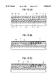
- FIGS. 12(A) to 12(C) and 13(A) and 13(B) are sectional views illustrating a method of producing the fourth embodiment of the present invention in order of steps;
- FIGS. 14(A) and 14(B) are plan views in different steps of the method of producing the fourth embodiment of the present invention, and wherein section 15--15 of FIG. 14(A) is the sectional view of FIG. 7(A) and section 15--15 of FIG. 14(B) is the sectional view of FIG. 8(A); and
- FIG. 15 is a sectional view showing a form wherein the fourth embodiment of the present invention is partially modified.
- FIGS. 6(A) and 6(B) show an essential part of the first embodiment of the present invention, wherein FIG. 6(A) is a plan view and FIG. 6(B) is a sectional view taken along line 6(B)--6(B) of FIG. 6(A),
- Insulation film 101 is provided on semiconductor substrate 100.
- Second conductive film patterns 2 in the form of a metal layer are formed on insulation film 101.
- Inter-layer insulation film 102 is formed on them.
- Contact holes 3 having elongated planar configurations and lead contact hole 3A are formed in inter-layer insulation film 102.
- First conductive film pattern 1 in the form of a metal layer having a spiral planar configuration is formed on inter-layer insulation film 102.
- This first conductive film pattern 1 is connected to second conductive film patterns 2 through contact holes 3.
- a spiral inductor element is composed of first and second conductive film patterns 1 and 2 described above.
- Second conductive film patterns 2 isolated from one another are electrically connected only to first conductive film pattern 1 of the spiral configuration. Further, one lead wiring 1A for the inductor element is formed continuously to first conductive film pattern 1 while the other lead wiring 2A of the inductor element is formed continuously to second conductive film patterns 2.
- Second conductive film patterns 2 are isolated patterns, that is, insular patterns, electrically connected only to first conductive film pattern 1. And, second conductive film patterns 2 are located just below first conductive film pattern 1 and connected to first conductive film pattern 1 through contact holes 3 and extend along first conductive film pattern 1.
- Lead wiring 2A formed from a metal layer of a lower layer similarly to second conductive film patterns 2 is connected to an end portion of first conductive film pattern 1 positioned at a central location of the spiral configuration and is led out to the outside of the spiral inductor element in such a manner that it does not contact second conductive film patterns 2.
- second conductive film patterns 2 and contact holes 3 are formed spaced away from lead wiring 2A and neighboring portions of lead wiring 2A so that second conductive film patterns 2 and lead wiring 2A may not be electrically short-circuited to each other.
- second conductive film patterns 2, lead wiring 2A and contact holes 3 and 3A of the lower layer are indicated by broken lines while first conductive film pattern 1 of the upper layer is indicated by solid lines. While, in the present embodiment, first conductive film pattern 1 and second conductive film patterns 2 extend with an equal width, in order to facilitate recognition, in the plan view of FIG. 6(A), second conductive film patterns 2 of the lower layer indicated by broken lines are shown with a greater width than first conductive film pattern 1 of the upper layer indicted by solid lines.
- second conductive film patterns 2 and contact holes 3 are formed under the substantially overall length of first conductive film pattern 1 of the spiral configuration except lead wiring 2A and the neighboring portions to lead wiring 2A, the arrangement substantially achieves increase in film thickness without increasing the effective length, and consequently, the resistance Rm of the inductor element can be reduced sufficiently. Further, since the layers are composed of the first and second conductive film patterns, there is no need of increasing the film thickness of each film, which facilitates patterning by etching or a like method.
- silicon oxide film 101 is deposited as an insulation film to a film thickness of 500 to 700 nm on the surface of semiconductor substrate 100 such as a silicon substrate using a CVD method. Then, using a sputtering method, a metal layer of a lower layer is formed to a thickness of 500 nm to 1 ⁇ m using, for example, aluminum, and then, using a photo-etching method, second conductive film patterns 2 isolated from each other and lead wiring 2A are formed by patterning.
- silicon oxide film 102 is deposited as an inter-layer insulation film to a film thickness of 500 nm to 1 ⁇ m by a CVD method, and contact holes 3 and lead contact hole 3A are formed using a dry etching method. Thereafter, a metal layer of the upper layer is formed to a thickness of 500 to 1 ⁇ m using, for example, aluminum, and using a photo-etching method, first conductive film pattern 1 of the spiral configuration and lead wiring 1A connected to first conductive film pattern 1 are formed by patterning.
- the parasitic resistance Rm can be reduced by constructing the body of the spiral inductor element from first conductive film pattern 1 of the upper layer and backing (aluminum backing) second conductive film patterns 2 of the lower layer to the body of the spiral inductor element.
- lead wiring 2A of the lower layer is used as a wiring for leading out one terminal of the inductor element from a central portion of the spiral wiring of first conductive film pattern 1.
- contact holes 3 in FIG. 6(A) of the present embodiment have elongated configurations, each of them may be an array of a large number of square contact holes.
- first and second conductive film patterns 1 and 2 form, at other locations on the semiconductor substrate, wirings which interconnect circuit elements in the LSI other than the spiral inductor.
- FIGS. 7(A) and 7(B) show an essential part of the second embodiment of the present invention, and wherein FIG. 7(A) is a plan view and FIG. 7(B) is a sectional view taken along line 7(B)--7(B) of FIG. 7(A). It is to be noted that, in FIGS. 7(A) and 7(B), same or similar elements are denoted by same reference characters to those of FIGS. 6(A) and 6(B) and overlapping description of them is omitted here.
- an inductor element can be realized which not only reduces the parasitic resistance of the inductor but also allows fine adjustment called trimming which is performed when a measured value of the inductance becomes displaced from a designed value therefor.
- first conductive film pattern 11 of a spiral configuration which serves as the body of an inductor element is formed from a metal layer of a lower layer while second conductive film patterns 12 for backing isolated from one another so as to reduce the resistance are formed from a metal layer of the upper layer.
- contact holes 3 having elongated planar configurations are formed in inter-layer insulation film 102 over the substantially overall length of first conductive film pattern 11 along second conductive film patterns 12.
- Second conductive film patterns 12 isolated one from the other are electrically connected only to first conductive film pattern 11 of the spiral configuration through contact holes 3.
- one lead wiring 12A and trimming conductive film 12B which serves as the other lead wiring are formed.
- the one lead wiring 12A extends through lead contact hole 3A and is connected to an end portion of first conductive film pattern 11 positioned at a central portion of the spiral configuration.
- Trimming conductive film 12B extends through lead contact holes 3B and is connected to an end portion of first conductive film pattern 11 positioned at an outermost peripheral portion of the spiral configuration, and serves as the other lead wiring. Further, trimming conductive film 12B extends through contact holes 3E and 3F and is connected to corresponding portions of first conductive film pattern 11.
- a selected one of X1 and X2 portions of trimming conductive film 12B is cut using a laser beam to adjust the inductance of the inductor element so as to have a desired inductance value, that is, trimming is performed. For example, if it is desired to maximize the inductor length, both of the X1 and X2 portions are cut. But if it is desired to minimize the inductor length, none of the X1 and X2 portions is cut.
- the one lead wiring 12A and trimming conductive film 12B which serves as the other lead wiring are led out to the outside of the spiral inductor element such that they do not contact with second conductive film patterns 12.
- second conductive film patterns 12 and contact holes 3 are formed each in a U-shaped planar configuration in a spaced relationship away from lead wiring 12A and trimming conductive film 12B and neighboring portions of them so that second conductive film patterns 12 may not be electrically short-circuited to lead wiring 12A or trimming conductive film 12B and may be connected to first conductive film pattern 11 over a distance as long as possible.
- second conductive film patterns 12, lead wiring 12A and trimming conductive film 12B of the upper layer are indicated by solid lines while first conductive film pattern 11 of the lower layer and contact holes 3, 3A, 3B, 3E and 3F are indicated by broken lines.
- first conductive film pattern 11 and second conductive film patterns 12 extend with an equal width, in order to facilitate recognition, in the plan view of FIG. 7(A), second conductive film patterns 12 of the upper layer indicated by solid lines are shown with a greater width than first conductive film pattern 11 indicated by solid lines.
- the first expression can be represented also like the following third expression.
- the dependency of the quality factor Q upon the frequency f exhibits such a characteristic as seen in FIG. 8 where the line width W is 15 ⁇ m, the line distance is 5 ⁇ m and the outer dimension a is 300 ⁇ m.
- the relationship between the dependency of the quality factor Q upon the frequency f and the parasitic components is such as illustrated in FIG. 8.
- the wiring resistance has a significant influence
- the factors of the parasitic capacitance Csub and the parasitic resistance Rsub have a significant influence.
- the first and second embodiments of the present invention are effective.
- the first to fourth embodiments may be adapted in a suitable combination.
- FIGS. 9(A) and 9(B) show an essential part of the third embodiment, wherein FIG. 9(A) is a plan view and FIG. 9(B) is a sectional view taken along line 9(B)--9(B) of FIG. 9(A). It is to be noted that, in FIGS. 9(A) and 9(B), same or similar elements are denoted by same reference characters to those of FIGS. 6(A) and 6(B), and therefore, overlapping description of them is omitted here.
- first conductive film pattern 1 of the spiral configuration and lead wiring 1A solid lines
- lead contact hole 3A broken line
- separation groove 4 alternate long and two short dashes lines
- the present third embodiment is different from the first and second embodiments described above in that an insulating separation region in which separation groove 4 in which insulation film 103 is filled is formed is provided in a substrate just below first conductive film pattern 1 of the spiral configuration which serves as the body of an inductor element provided on an insulation film on the substrate.
- the parasitic capacitance produced between the inductor element and the substrate can be reduced to a very low value by insulating separation region 4, 103 provided in the substrate.
- an insulation film such as, for example, silicon oxide film 101 is formed to a film thickness of 500 to 700 nm on semiconductor substrate 100 as seen in FIG. 10(A).
- semiconductor substrate 100 and silicon oxide film 101 are dry etched to form separation groove 4 of, for example, 5 ⁇ m deep as seen in FIG. 10(B).
- the width of separation groove 4 is equal to or greater by 1 to 2 ⁇ m than the width of an inductor wiring which is formed at a later step, that is, the width of the first conductive film pattern.
- an inductor wiring pattern that is, the first conductive film pattern is wide, a plurality of separation grooves can be provided just under the first conductive film pattern.
- silicon oxide film 103 is deposited to a thickness of 500 nm to 1 ⁇ m as seen in FIG. 10(C) by a CVD method.
- Silicon oxide film 103 is used as an inter-layer insulation film under second conductive film patterns 2 and lead wiring 2A of the lower layer metal layer and also as an insulation film for filling up the inside of separation groove 4.
- the surface of silicon oxide film 103 may be polished by a CMP (Chemical-Mechanical-Polishing) method to enhance the flatness of the surface.
- CMP Chemical-Mechanical-Polishing
- first conductive film 1 of the spiral configuration which serves as the body of the spiral inductor element is formed just above separation groove 4.
- the second conductive film patterns of the insular configuration are the conductive film patterns of the lower layer formed on separation groove region 4 while the first conductive film pattern of the spiral configuration is the conductive film pattern of the upper layer provided on the second conductive patterns with the inter-layer insulation film interposed therebetween.
- the first conductive film pattern of the spiral configuration may be the conductive film pattern of the lower layer formed on separation groove region 4 while the second conductive film patterns of the insular configuration may be the conductive film pattern of the upper layer provided on the first conductive film pattern with the inter-layer insulation film interposed therebetween.
- similar effects can be achieved.
- the reason why not one groove conforming to the outer profile of the inductor element is provided but separate groove regions are provided in the substrate just below the body of the inductor element along the inductor pattern of the spiral configuration is that it is intended to facilitate filling up of the inside of the separation groove with the insulation film.
- the outer profile of the inductor element normally has such a size of up to several hundreds ⁇ m square as described hereinabove, and it is very difficult to fill up over such a large area with a good flatness with an insulation film.
- the grooves provided under the inductor element and separation grooves for transistor elements used in the inside of a circuit provided in another region of the LSI are formed simultaneously, if a groove region of the spiral configuration is provided in the substrate under the inductance element as in the present embodiment, then the insides of the grooves can be filled up readily with an insulation film.
- the groove separation for bipolar transistors is provided with the width of 0.5 to 1.5 ⁇ m and the depth of 3 to 5 ⁇ m.
- a semiconductor substrate in which a groove is to be formed, it is important for a semiconductor substrate, in which a groove is to be formed, to have a resistance as high as possible (high Rsub) as seen from the third expression described above. Accordingly, for example, a substrate having a specific resistance of 10 to 100 ohm-cm is used.
- FIGS. 11(A) and 11(B) show an essential part of the fourth embodiment, and wherein FIG. 11(A) is a plan view and FIG. 11(B) is a sectional view taken along line 11(B)--11(B) of FIG. 11(A). It is to be noted that, in FIGS. 11(A) and 11(B), same or similar elements are denoted by same reference characters to those of FIGS. 6(A) and 6(B), and therefore, overlapping description of them is omitted here.
- the present fourth embodiment is different from the first to third embodiments in that a spiral inductor provided on an insulation film on a substrate has side walls of a magnetic substance layer on side faces of first conductive film pattern 1 of the spiral configuration of the upper layer which is the body of the inductor element with insulation films interposed therebetween.
- first conductive film pattern 1, lead wiring 1A and magnetic substance side walls 5 formed from the metal layer of the upper layer are shown.
- lower layer wirings 16 obtained, upon formation of mutually isolated second conductive film patterns 2 of the inductor element, by patterning of the metal layer of the same lower layer and upper layer wirings 17 obtained, upon formation of first conductive film pattern 1 of the spiral configuration of the inductor element, by patterning of the metal layer of the same upper layer are formed. And, upper layer wirings 17 and lower layer wirings 16 are connected to each other through through-holes 18 formed at the same step as that of formation of contact holes 3 of the inductor element. Thus, a multi-layer wiring structure for the other internal circuits of the semiconductor substrate is constructed from them.
- insulation films for example, silicon oxide films 104 and 105, are provided on first conductive film pattern 1 of the inductor element and upper layer wirings 17 of the multi-layer wiring structure, respectively, and silicon oxide film 105 is applied to side faces of first conductive film pattern 1 of the spiral configuration of the inductor element and side walls 5 of a magnetic substance layer are formed on silicon oxide film 105.
- an insulation film for example, silicon oxide film 101
- a lower layer metal layer is deposited and patterned to form mutually isolated second conductive film patterns 2 and lead wiring 2A of the spiral inductor element and lower layer wirings 16 for the other internal circuits.
- an insulation film for example, silicon oxide film 102
- a low temperature CVD method of a growth temperature of 200° to 400° C.
- upper layer metal layer 19 and an insulation film are formed to a film thickness of 200 to 300 nm.
- Silicon oxide film 104 on upper layer metal layer 19 is provided to facilitate etching of upper layer metal layer 19 and need not necessarily be provided.
- silicon oxide film 104 and upper layer metal layer 19 are selectively etched using photo-resist 6 as a mask to form space groove 7 for an inductor element. If, upon this etching, also inter-layer insulation film 102 below is over etched by 100 to 200 nm, then magnetic substance side walls to be formed in a following step can be formed on and cover over the side faces of first conductive film pattern 1 of the spiral configuration sufficiently and readily.
- FIG. 12(A) a structure shown in the sectional view of FIG. 12(A) is obtained. Further, a plan view only of space groove 7 in this instance is shown in FIG. 14(A), and a sectional view taken along line 15--15 of FIG. 14(A) is FIG. 12(A).
- an insulation film for example, silicon oxide film 105
- an insulation film for example, silicon oxide film 105
- a low temperature CVD method at a growth temperature of 200 to 450° C.
- a magnetic substance layer for example, alloy layer 9 of an iron-nickel (Fe ⁇ Ni) alloy is formed.
- the milling conditions are: for example, an acceleration voltage of 400 to 500 V and an acceleration current of 0.4 to 0.5 A.
- FIG. 13(A) A plan view in this instance is shown in FIG. 14(B), and a sectional view taken along line 15--15 of FIG. 14(B) is FIG. 13(A).
- etching mask 21 is removed, thereby to obtain a structure shown in the sectional view of FIG. 13(B).
- the space between the first conductive films of the spiral configuration of the spiral inductor element may otherwise be filled up fully with magnetic substance layer 5 as seen in FIG. 15.
- an iron-nickel alloy has a superior frequency characteristic and a magnetic substance layer of the alloy can be used for a region of several MHz to several tens MHz.
- cobalt may be mixed into a magnetic substance layer to form an alloy layer of iron-nickel-cobalt (Fe ⁇ Ni ⁇ Co).
- the iron-nickel-cobalt alloy is higher in frequency characteristic than the iron-nickel alloy and can be used for a radio frequency of several hundreds MHz or more.
- the silicon oxide films as insulation films 101, 102, 103, 104 and 105 employed in the first to fourth embodiments described above preferably contain no impurity such as phosphor in order to eliminate an influence of depolarization or a like phenomenon.
- the material of those insulation films is not limited to silicon oxide films, and some other insulation materials such as silicon nitride films may be employed or those insulation materials may be combined suitably to construct insulation films.
- the parasitic resistance Rm of a spiral inductor element can be reduced remarkably.
- the parasitic capacitance produced between the inductor element and the substrate can be reduced to a very low value while the quality factor Q of the inductor element can be raised high.
- a magnetic substance layer can be provided between wiring layers of a spiral inductor element more readily than by methods of production proposed conventionally, and the value of the quality factor Q of the inductor can be further raised and a good high frequency characteristic can be obtained.
Landscapes
- Semiconductor Integrated Circuits (AREA)
- Coils Or Transformers For Communication (AREA)
Applications Claiming Priority (2)
| Application Number | Priority Date | Filing Date | Title |
|---|---|---|---|
| JP7-341515 | 1995-12-27 | ||
| JP7341515A JP2904086B2 (ja) | 1995-12-27 | 1995-12-27 | 半導体装置およびその製造方法 |
Publications (1)
| Publication Number | Publication Date |
|---|---|
| US6002161A true US6002161A (en) | 1999-12-14 |
Family
ID=18346667
Family Applications (1)
| Application Number | Title | Priority Date | Filing Date |
|---|---|---|---|
| US08/756,536 Expired - Fee Related US6002161A (en) | 1995-12-27 | 1996-11-26 | Semiconductor device having inductor element made of first conductive layer of spiral configuration electrically connected to second conductive layer of insular configuration |
Country Status (4)
| Country | Link |
|---|---|
| US (1) | US6002161A (de) |
| EP (1) | EP0782190A3 (de) |
| JP (1) | JP2904086B2 (de) |
| KR (1) | KR100267413B1 (de) |
Cited By (81)
| Publication number | Priority date | Publication date | Assignee | Title |
|---|---|---|---|---|
| US6143614A (en) * | 1996-02-29 | 2000-11-07 | Texas Instruments Incorporated | Monolithic inductor |
| US6169320B1 (en) * | 1998-01-22 | 2001-01-02 | Raytheon Company | Spiral-shaped inductor structure for monolithic microwave integrated circuits having air gaps in underlying pedestal |
| US6201287B1 (en) * | 1998-10-26 | 2001-03-13 | Micron Technology, Inc. | Monolithic inductance-enhancing integrated circuits, complementary metal oxide semiconductor (CMOS) inductance-enhancing integrated circuits, inductor assemblies, and inductance-multiplying methods |
| US6287931B1 (en) * | 1998-12-04 | 2001-09-11 | Winbond Electronics Corp. | Method of fabricating on-chip inductor |
| US6373121B1 (en) * | 2001-03-23 | 2002-04-16 | United Microelectronics Corp. | Silicon chip built-in inductor structure |
| KR20020039016A (ko) * | 2000-11-20 | 2002-05-25 | 황인길 | 멀티라인구조를 갖는 나선형 인덕터 및 제조방법 |
| US6395637B1 (en) * | 1997-12-03 | 2002-05-28 | Electronics And Telecommunications Research Institute | Method for fabricating a inductor of low parasitic resistance and capacitance |
| US6429504B1 (en) * | 2000-05-16 | 2002-08-06 | Tyco Electronics Corporation | Multilayer spiral inductor and integrated circuits incorporating the same |
| US6504227B1 (en) * | 1999-06-30 | 2003-01-07 | Kabushiki Kaisha Toshiba | Passive semiconductor device mounted as daughter chip on active semiconductor device |
| US20030005572A1 (en) * | 1999-11-23 | 2003-01-09 | Gardner Donald S. | Integrated inductor |
| US6531929B2 (en) | 1998-11-23 | 2003-03-11 | Micron Technology, Inc. | Monolithic integrated circuit oscillators, complementary metal oxide semiconductor (cmos) voltage-controlled oscillators, integrated circuit oscillators, oscillator-forming methods, and oscillation methods |
| US6534842B2 (en) * | 1998-03-03 | 2003-03-18 | Matsushita Electric Industrial Co., Ltd. | Composite components and the method of manufacturing the same |
| US6545354B1 (en) | 1999-02-15 | 2003-04-08 | Casio Computer Co., Ltd. | Semiconductor device having a barrier layer |
| US20030127704A1 (en) * | 2001-12-14 | 2003-07-10 | Kazuhiko Kobayashi | Electronic device |
| US6608361B2 (en) * | 2001-07-31 | 2003-08-19 | G-Plus, Inc. | On-chip inductor using active magnetic energy recovery |
| US6650220B2 (en) * | 2002-04-23 | 2003-11-18 | Chartered Semiconductor Manufacturing Ltd. | Parallel spiral stacked inductor on semiconductor material |
| US20040100349A1 (en) * | 2002-11-14 | 2004-05-27 | Bongki Mheen | Inductor having high quality factor and unit inductor arranging method therefor |
| US20040119574A1 (en) * | 2002-09-13 | 2004-06-24 | Lee Kwang-Du | Inductor for radio frequency integrated circuit |
| US20040171227A1 (en) * | 2000-09-28 | 2004-09-02 | Kabushiki Kaisha Toshiba | Semiconductor device with spiral inductor and method for fabricating semiconductor integrated circuit device |
| US20040212039A1 (en) * | 2003-04-28 | 2004-10-28 | Nec Electronics Corporation | Semiconductor device |
| EP1480234A2 (de) * | 2003-05-21 | 2004-11-24 | Texas Instruments Incorporated | Induktivität für integrierte Schaltkreise mit integrierten Verbindungsleitern |
| US6833285B1 (en) * | 1999-02-01 | 2004-12-21 | Micron Technology, Inc. | Method of making a chip packaging device having an interposer |
| US6847066B2 (en) * | 2000-08-11 | 2005-01-25 | Oki Electric Industry Co., Ltd. | Semiconductor device |
| US20050030144A1 (en) * | 2003-08-07 | 2005-02-10 | Tdk Corporation | Coil component |
| US20050074905A1 (en) * | 2003-10-01 | 2005-04-07 | Yong-Geun Lee | Inductors in semiconductor devices and methods of manufacturing the same |
| US20050073025A1 (en) * | 2003-02-04 | 2005-04-07 | Mitsubishi Denki Kabushiki Kaisha | Spiral inductor and transformer |
| US20050099259A1 (en) * | 2003-09-30 | 2005-05-12 | Harris Edward B. | Inductor formed in an integrated circuit |
| US20050104158A1 (en) * | 2003-11-19 | 2005-05-19 | Scintera Networks, Inc. | Compact, high q inductor for integrated circuit |
| US20050104705A1 (en) * | 2003-11-19 | 2005-05-19 | Scintera Networks, Inc. | Multi-layer symmetric inductor |
| US20050174209A1 (en) * | 2003-11-14 | 2005-08-11 | Canon Kabushiki Kaisha | Wiring structure, and fabrication method of the same |
| US20050184358A1 (en) * | 1998-12-21 | 2005-08-25 | Megic Corporation | High performance system-on-chip using post passivation process |
| US20060163694A1 (en) * | 2004-12-27 | 2006-07-27 | Kabushiki Kaisha Toshiba | Semiconductor device having spiral-shaped inductor |
| US20060234459A1 (en) * | 2005-04-18 | 2006-10-19 | Oki Electric Industry Co., Ltd. | Semiconductor device and method for manufacturing the same |
| US20070107206A1 (en) * | 2003-08-22 | 2007-05-17 | Harris Edward B | Spiral Inductor Formed in a Semiconductor Substrate and a Method for Forming the Inductor |
| US20070182521A1 (en) * | 2003-05-27 | 2007-08-09 | Megica Corporation | High performance system-on-chip inductor using post passivation process |
| US20070239444A1 (en) * | 2006-03-29 | 2007-10-11 | Motorola, Inc. | Voice signal perturbation for speech recognition |
| US7312685B1 (en) * | 2006-09-11 | 2007-12-25 | Via Technologies, Inc. | Symmetrical inductor |
| US20080100408A1 (en) * | 2006-10-25 | 2008-05-01 | Chih-Hua Chen | Inductor structure |
| US20090045903A1 (en) * | 2007-08-17 | 2009-02-19 | Via Technologies, Inc. | Inductor structure |
| US20090096566A1 (en) * | 2007-10-12 | 2009-04-16 | Via Technologies, Inc. | Spiral inductor device |
| US20090104769A1 (en) * | 2005-05-18 | 2009-04-23 | Megica Corporation | Semiconductor chip with coil element over passivation layer |
| US20090261452A1 (en) * | 2008-04-18 | 2009-10-22 | Tsujimoto Kouichi | Semiconductor device including an inductor element |
| US20100230783A1 (en) * | 2009-03-13 | 2010-09-16 | Nec Electronics Corporation | Semiconductor device |
| US20100327406A1 (en) * | 2009-06-26 | 2010-12-30 | Stats Chippac, Ltd. | Semiconductor Device and Method of Forming Inductor Over Insulating Material Filled Trench In Substrate |
| US7863654B2 (en) | 1998-12-21 | 2011-01-04 | Megica Corporation | Top layers of metal for high performance IC's |
| US7960269B2 (en) | 2005-07-22 | 2011-06-14 | Megica Corporation | Method for forming a double embossing structure |
| US20110156854A1 (en) * | 2007-10-12 | 2011-06-30 | Via Technologies, Inc. | Spiral Inductor Device |
| US7973629B2 (en) | 2001-09-04 | 2011-07-05 | Megica Corporation | Method for making high-performance RF integrated circuits |
| US8008775B2 (en) | 2004-09-09 | 2011-08-30 | Megica Corporation | Post passivation interconnection structures |
| US8018060B2 (en) | 2004-09-09 | 2011-09-13 | Megica Corporation | Post passivation interconnection process and structures |
| US20110227689A1 (en) * | 2007-11-29 | 2011-09-22 | Taiwan Semiconductor Manufacturing Co., Ltd. | Method of Creating Spiral Inductor having High Q Value |
| CN102237336A (zh) * | 2010-05-05 | 2011-11-09 | Nxp股份有限公司 | 集成变压器 |
| US8178435B2 (en) | 1998-12-21 | 2012-05-15 | Megica Corporation | High performance system-on-chip inductor using post passivation process |
| US20120146273A1 (en) * | 2009-04-22 | 2012-06-14 | Tiefenboeck Herbert | Receiving device for receiving semiconductor substrates |
| US20120151748A1 (en) * | 2008-03-26 | 2012-06-21 | International Business Machines Corporation | Methods of designing an inductor having opening enclosed within conductive line |
| US20120306092A1 (en) * | 2010-11-15 | 2012-12-06 | Tessera, Inc. | Conductive pads defined by embedded traces |
| US8384189B2 (en) | 2005-03-29 | 2013-02-26 | Megica Corporation | High performance system-on-chip using post passivation process |
| US8421158B2 (en) | 1998-12-21 | 2013-04-16 | Megica Corporation | Chip structure with a passive device and method for forming the same |
| US20130140717A1 (en) * | 2010-03-31 | 2013-06-06 | Renesas Electronics Corporation | Semiconductor device |
| US20130146345A1 (en) * | 2011-12-12 | 2013-06-13 | Kazuki KAJIHARA | Printed wiring board and method for manufacturing the same |
| US20140070915A1 (en) * | 2006-03-03 | 2014-03-13 | Seiko Epson Corporation | Electronic substrate, semiconductor device, and electronic device |
| US8709831B2 (en) | 2010-10-07 | 2014-04-29 | Infineon Technologies Ag | Integrated circuits with magnetic core inductors and methods of fabrications thereof |
| US8717136B2 (en) | 2012-01-10 | 2014-05-06 | International Business Machines Corporation | Inductor with laminated yoke |
| US8749021B2 (en) | 2006-12-26 | 2014-06-10 | Megit Acquisition Corp. | Voltage regulator integrated with semiconductor chip |
| US8809951B2 (en) | 2008-12-26 | 2014-08-19 | Megit Acquisition Corp. | Chip packages having dual DMOS devices with power management integrated circuits |
| US8809190B2 (en) | 2010-09-17 | 2014-08-19 | Tessera, Inc. | Multi-function and shielded 3D interconnects |
| US8847380B2 (en) | 2010-09-17 | 2014-09-30 | Tessera, Inc. | Staged via formation from both sides of chip |
| US9064628B2 (en) | 2012-05-22 | 2015-06-23 | International Business Machines Corporation | Inductor with stacked conductors |
| US9070678B2 (en) | 2006-11-22 | 2015-06-30 | Tessera, Inc. | Packaged semiconductor chips with array |
| US9099296B2 (en) | 2010-12-02 | 2015-08-04 | Tessera, Inc. | Stacked microelectronic assembly with TSVS formed in stages with plural active chips |
| US20160012952A1 (en) * | 2013-10-02 | 2016-01-14 | Globalfoundries Inc. | Inductor structure having embedded airgap |
| US9269692B2 (en) | 2010-12-02 | 2016-02-23 | Tessera, Inc. | Stacked microelectronic assembly with TSVS formed in stages and carrier above chip |
| US20160064470A1 (en) * | 2014-09-03 | 2016-03-03 | Teledyne Scientific & Imaging, Llc | Micro-fabricated integrated coil and magnetic circuit and method of manufacturing thereof |
| US20160328080A1 (en) * | 2015-05-04 | 2016-11-10 | Semiconductor Energy Laboratory Co., Ltd. | Touch panel and data processor |
| US9640437B2 (en) | 2010-07-23 | 2017-05-02 | Tessera, Inc. | Methods of forming semiconductor elements using micro-abrasive particle stream |
| US20170317506A1 (en) * | 2012-03-29 | 2017-11-02 | Samsung Electro-Mechanics Co., Ltd. | Thin film coil and electronic device having the same |
| US10062505B1 (en) * | 2015-12-30 | 2018-08-28 | Hrl Laboratories, Llc | Laminated conductors |
| US20190057942A1 (en) * | 2017-08-16 | 2019-02-21 | Texas Instruments Incorporated | Integrated circuit with an embedded inductor or transformer |
| US10553353B2 (en) * | 2016-11-18 | 2020-02-04 | Globalfoundries Inc. | Parallel stacked inductor for high-Q and high current handling and method of making the same |
| US11183471B2 (en) * | 2019-11-12 | 2021-11-23 | Renesas Electronics Corporation | Semiconductor device |
| US11437173B2 (en) * | 2017-09-05 | 2022-09-06 | Samsung Electro-Mechanics Co., Ltd. | Coil component |
Families Citing this family (21)
| Publication number | Priority date | Publication date | Assignee | Title |
|---|---|---|---|---|
| US5861647A (en) * | 1996-10-02 | 1999-01-19 | National Semiconductor Corporation | VLSI capacitors and high Q VLSI inductors using metal-filled via plugs |
| KR19990055422A (ko) * | 1997-12-27 | 1999-07-15 | 정선종 | 실리콘 기판에서의 인덕터 장치 및 그 제조 방법 |
| NL1008353C2 (nl) * | 1998-02-19 | 1999-08-20 | Nedap Nv | Spoel- en verbindingsconstructie voor een contactloos label. |
| JP3942264B2 (ja) | 1998-03-11 | 2007-07-11 | 富士通株式会社 | 半導体基板上に形成されるインダクタンス素子 |
| SE512699C2 (sv) * | 1998-03-24 | 2000-05-02 | Ericsson Telefon Ab L M | En induktansanordning |
| FR2780551B1 (fr) * | 1998-06-29 | 2001-09-07 | Inside Technologies | Micromodule electronique integre et procede de fabrication d'un tel micromodule |
| FR2780546B1 (fr) * | 1998-06-29 | 2003-05-16 | Memscap | Circuit integre monolithique comprenant une inductance plane ou un transformateur plan, et procede de fabrication d'un tel circuit |
| EP0991123A1 (de) * | 1998-10-01 | 2000-04-05 | EM Microelectronic-Marin SA | Mikrostruktur mit einer magnetischen Antenne oder einem magnetischen Detector |
| FR2791470B1 (fr) * | 1999-03-23 | 2001-06-01 | Memscap | Circuit integre monolithique incorporant un composant inductif et procede de fabrication d'un tel circuit integre |
| KR100348247B1 (ko) * | 1999-09-21 | 2002-08-09 | 엘지전자 주식회사 | 마이크로 수동소자 및 제조 방법 |
| DE10040811A1 (de) * | 2000-08-21 | 2002-03-14 | Infineon Technologies Ag | Monolithisch integrierbare Induktivität |
| KR100420948B1 (ko) * | 2001-08-22 | 2004-03-02 | 한국전자통신연구원 | 병렬 분기 구조의 나선형 인덕터 |
| WO2003038899A2 (de) * | 2001-10-26 | 2003-05-08 | Infineon Technologies Ag | Halbleiterstruktur mit einer spule unter der ersten verdrahtungsschicht oder zwischen zwei verdrahtungsschichten |
| US6841847B2 (en) * | 2002-09-04 | 2005-01-11 | Chartered Semiconductor Manufacturing, Ltd. | 3-D spiral stacked inductor on semiconductor material |
| KR100937648B1 (ko) * | 2002-12-30 | 2010-01-19 | 동부일렉트로닉스 주식회사 | 반도체 인덕터 및 이의 제조 방법 |
| US7750413B2 (en) | 2003-06-16 | 2010-07-06 | Nec Corporation | Semiconductor device and method for manufacturing same |
| JP4668719B2 (ja) * | 2005-07-25 | 2011-04-13 | Okiセミコンダクタ株式会社 | インダクタの特性調整方法 |
| US7636242B2 (en) | 2006-06-29 | 2009-12-22 | Intel Corporation | Integrated inductor |
| JP5090688B2 (ja) * | 2006-08-17 | 2012-12-05 | ルネサスエレクトロニクス株式会社 | 半導体装置 |
| KR100818411B1 (ko) * | 2007-03-26 | 2008-04-02 | 동부일렉트로닉스 주식회사 | 온 칩 인덕터 구조 및 방법 |
| US20090115022A1 (en) * | 2007-11-06 | 2009-05-07 | Nec Electronics Coroporation | Semiconductor device |
Citations (6)
| Publication number | Priority date | Publication date | Assignee | Title |
|---|---|---|---|---|
| JPS61144052A (ja) * | 1984-12-17 | 1986-07-01 | Mitsubishi Electric Corp | 半導体装置 |
| US4959631A (en) * | 1987-09-29 | 1990-09-25 | Kabushiki Kaisha Toshiba | Planar inductor |
| JPH03263366A (ja) * | 1990-03-13 | 1991-11-22 | Fujitsu Ltd | 半導体装置及びその製造方法 |
| US5384274A (en) * | 1992-04-06 | 1995-01-24 | Nippon Precision Circuits Inc. | Method of making a combined semiconductor device and inductor |
| US5610433A (en) * | 1995-03-13 | 1997-03-11 | National Semiconductor Corporation | Multi-turn, multi-level IC inductor with crossovers |
| US5793272A (en) * | 1996-08-23 | 1998-08-11 | International Business Machines Corporation | Integrated circuit toroidal inductor |
Family Cites Families (7)
| Publication number | Priority date | Publication date | Assignee | Title |
|---|---|---|---|---|
| JPS59114807A (ja) * | 1982-12-21 | 1984-07-03 | Matsushita Electric Ind Co Ltd | プリント多層コイル |
| JPH0377360A (ja) * | 1989-08-18 | 1991-04-02 | Mitsubishi Electric Corp | 半導体装置 |
| JPH07106514A (ja) * | 1993-10-07 | 1995-04-21 | Toshiba Corp | 半導体集積回路装置 |
| JPH07211865A (ja) * | 1994-01-19 | 1995-08-11 | Fujitsu Ltd | インダクタ |
| JPH07240502A (ja) * | 1994-03-02 | 1995-09-12 | Hitachi Ltd | 半導体集積回路装置およびその製造方法 |
| GB2292015B (en) * | 1994-07-29 | 1998-07-22 | Plessey Semiconductors Ltd | Trimmable inductor structure |
| US5446311A (en) * | 1994-09-16 | 1995-08-29 | International Business Machines Corporation | High-Q inductors in silicon technology without expensive metalization |
-
1995
- 1995-12-27 JP JP7341515A patent/JP2904086B2/ja not_active Expired - Fee Related
-
1996
- 1996-11-07 EP EP96117885A patent/EP0782190A3/de not_active Withdrawn
- 1996-11-26 US US08/756,536 patent/US6002161A/en not_active Expired - Fee Related
- 1996-12-13 KR KR1019960065055A patent/KR100267413B1/ko not_active Expired - Fee Related
Patent Citations (6)
| Publication number | Priority date | Publication date | Assignee | Title |
|---|---|---|---|---|
| JPS61144052A (ja) * | 1984-12-17 | 1986-07-01 | Mitsubishi Electric Corp | 半導体装置 |
| US4959631A (en) * | 1987-09-29 | 1990-09-25 | Kabushiki Kaisha Toshiba | Planar inductor |
| JPH03263366A (ja) * | 1990-03-13 | 1991-11-22 | Fujitsu Ltd | 半導体装置及びその製造方法 |
| US5384274A (en) * | 1992-04-06 | 1995-01-24 | Nippon Precision Circuits Inc. | Method of making a combined semiconductor device and inductor |
| US5610433A (en) * | 1995-03-13 | 1997-03-11 | National Semiconductor Corporation | Multi-turn, multi-level IC inductor with crossovers |
| US5793272A (en) * | 1996-08-23 | 1998-08-11 | International Business Machines Corporation | Integrated circuit toroidal inductor |
Cited By (164)
| Publication number | Priority date | Publication date | Assignee | Title |
|---|---|---|---|---|
| US6143614A (en) * | 1996-02-29 | 2000-11-07 | Texas Instruments Incorporated | Monolithic inductor |
| US6395637B1 (en) * | 1997-12-03 | 2002-05-28 | Electronics And Telecommunications Research Institute | Method for fabricating a inductor of low parasitic resistance and capacitance |
| US6169320B1 (en) * | 1998-01-22 | 2001-01-02 | Raytheon Company | Spiral-shaped inductor structure for monolithic microwave integrated circuits having air gaps in underlying pedestal |
| US6258652B1 (en) | 1998-01-22 | 2001-07-10 | Raytheon Company | Spiral-shaped inductor structure for monolithic microwave integrated circuits having air gaps in underlying pedestal |
| US6534842B2 (en) * | 1998-03-03 | 2003-03-18 | Matsushita Electric Industrial Co., Ltd. | Composite components and the method of manufacturing the same |
| US6201287B1 (en) * | 1998-10-26 | 2001-03-13 | Micron Technology, Inc. | Monolithic inductance-enhancing integrated circuits, complementary metal oxide semiconductor (CMOS) inductance-enhancing integrated circuits, inductor assemblies, and inductance-multiplying methods |
| US6680518B2 (en) | 1998-10-26 | 2004-01-20 | Micron Technology, Inc. | Monolithic inductance-enhancing integrated circuits, complementary metal oxide semiconductor (CMOS) inductance-enhancing integrated circuits, inductor assemblies, and inductance-multiplying methods |
| US6593201B2 (en) | 1998-10-26 | 2003-07-15 | Micron Technology, Inc. | Monolithic inductance-enhancing integrated circuits, complementary metal oxide semiconductor (CMOS) inductance-enhancing integrated circuits, inductor assemblies, and inductance-multiplying methods |
| US6531929B2 (en) | 1998-11-23 | 2003-03-11 | Micron Technology, Inc. | Monolithic integrated circuit oscillators, complementary metal oxide semiconductor (cmos) voltage-controlled oscillators, integrated circuit oscillators, oscillator-forming methods, and oscillation methods |
| US6287931B1 (en) * | 1998-12-04 | 2001-09-11 | Winbond Electronics Corp. | Method of fabricating on-chip inductor |
| US20070181970A1 (en) * | 1998-12-21 | 2007-08-09 | Megica Corporation | High performance system-on-chip inductor using post passivation process |
| US20080035972A1 (en) * | 1998-12-21 | 2008-02-14 | Megica Corporation | High performance system-on-chip using post passivation process |
| US8415800B2 (en) | 1998-12-21 | 2013-04-09 | Megica Corporation | Top layers of metal for high performance IC's |
| US8421158B2 (en) | 1998-12-21 | 2013-04-16 | Megica Corporation | Chip structure with a passive device and method for forming the same |
| US20050184358A1 (en) * | 1998-12-21 | 2005-08-25 | Megic Corporation | High performance system-on-chip using post passivation process |
| US7422941B2 (en) | 1998-12-21 | 2008-09-09 | Megica Corporation | High performance system-on-chip using post passivation process |
| US8178435B2 (en) | 1998-12-21 | 2012-05-15 | Megica Corporation | High performance system-on-chip inductor using post passivation process |
| US7863654B2 (en) | 1998-12-21 | 2011-01-04 | Megica Corporation | Top layers of metal for high performance IC's |
| US20080044976A1 (en) * | 1998-12-21 | 2008-02-21 | Megica Corporation | High performance system-on-chip using post passivation process |
| US7884479B2 (en) | 1998-12-21 | 2011-02-08 | Megica Corporation | Top layers of metal for high performance IC's |
| US20080038869A1 (en) * | 1998-12-21 | 2008-02-14 | Megica Corporation | High performance system-on-chip using post passivation process |
| US7459761B2 (en) * | 1998-12-21 | 2008-12-02 | Megica Corporation | High performance system-on-chip using post passivation process |
| US7999384B2 (en) | 1998-12-21 | 2011-08-16 | Megica Corporation | Top layers of metal for high performance IC's |
| US8531038B2 (en) | 1998-12-21 | 2013-09-10 | Megica Corporation | Top layers of metal for high performance IC's |
| US8471384B2 (en) | 1998-12-21 | 2013-06-25 | Megica Corporation | Top layers of metal for high performance IC's |
| US8022545B2 (en) | 1998-12-21 | 2011-09-20 | Megica Corporation | Top layers of metal for high performance IC's |
| US8487400B2 (en) | 1998-12-21 | 2013-07-16 | Megica Corporation | High performance system-on-chip using post passivation process |
| US6833285B1 (en) * | 1999-02-01 | 2004-12-21 | Micron Technology, Inc. | Method of making a chip packaging device having an interposer |
| US6870256B2 (en) | 1999-02-15 | 2005-03-22 | Casio Computer Co., Ltd. | Semiconductor device having a thin-film circuit element provided above an integrated circuit |
| USRE41511E1 (en) | 1999-02-15 | 2010-08-17 | Casio Computer Co., Ltd. | Semiconductor device having a thin-film circuit element provided above an integrated circuit |
| US6545354B1 (en) | 1999-02-15 | 2003-04-08 | Casio Computer Co., Ltd. | Semiconductor device having a barrier layer |
| US6504227B1 (en) * | 1999-06-30 | 2003-01-07 | Kabushiki Kaisha Toshiba | Passive semiconductor device mounted as daughter chip on active semiconductor device |
| US6933205B2 (en) | 1999-06-30 | 2005-08-23 | Kabushiki Kaisha Toshiba | Integrated circuit device and method of manufacturing the same |
| US7982574B2 (en) | 1999-11-23 | 2011-07-19 | Intel Corporation | Integrated transformer |
| US7064646B2 (en) * | 1999-11-23 | 2006-06-20 | Intel Corporation | Integrated inductor |
| US20030005572A1 (en) * | 1999-11-23 | 2003-01-09 | Gardner Donald S. | Integrated inductor |
| US20100295649A1 (en) * | 1999-11-23 | 2010-11-25 | Gardner Donald S | Integrated transformer |
| US20050146411A1 (en) * | 1999-11-23 | 2005-07-07 | Gardner Donald S. | Integrated inductor |
| US6988307B2 (en) | 1999-11-23 | 2006-01-24 | Intel Corporation | Method of making an integrated inductor |
| US6429504B1 (en) * | 2000-05-16 | 2002-08-06 | Tyco Electronics Corporation | Multilayer spiral inductor and integrated circuits incorporating the same |
| US6847066B2 (en) * | 2000-08-11 | 2005-01-25 | Oki Electric Industry Co., Ltd. | Semiconductor device |
| US20040171227A1 (en) * | 2000-09-28 | 2004-09-02 | Kabushiki Kaisha Toshiba | Semiconductor device with spiral inductor and method for fabricating semiconductor integrated circuit device |
| US6951794B2 (en) * | 2000-09-28 | 2005-10-04 | Kabushiki Kaisha Toshiba | Semiconductor device with spiral inductor and method for fabricating semiconductor integrated circuit device |
| KR20020039016A (ko) * | 2000-11-20 | 2002-05-25 | 황인길 | 멀티라인구조를 갖는 나선형 인덕터 및 제조방법 |
| US6373121B1 (en) * | 2001-03-23 | 2002-04-16 | United Microelectronics Corp. | Silicon chip built-in inductor structure |
| US6608361B2 (en) * | 2001-07-31 | 2003-08-19 | G-Plus, Inc. | On-chip inductor using active magnetic energy recovery |
| US8384508B2 (en) | 2001-09-04 | 2013-02-26 | Megica Corporation | Method for making high-performance RF integrated circuits |
| US7973629B2 (en) | 2001-09-04 | 2011-07-05 | Megica Corporation | Method for making high-performance RF integrated circuits |
| US7064645B2 (en) * | 2001-12-14 | 2006-06-20 | Fujitsu Limited | Electronic device |
| US20030127704A1 (en) * | 2001-12-14 | 2003-07-10 | Kazuhiko Kobayashi | Electronic device |
| US6650220B2 (en) * | 2002-04-23 | 2003-11-18 | Chartered Semiconductor Manufacturing Ltd. | Parallel spiral stacked inductor on semiconductor material |
| US7205876B2 (en) | 2002-09-13 | 2007-04-17 | Samsung Electronics Co., Ltd. | Inductor for radio frequency integrated circuit |
| US20040119574A1 (en) * | 2002-09-13 | 2004-06-24 | Lee Kwang-Du | Inductor for radio frequency integrated circuit |
| US20040100349A1 (en) * | 2002-11-14 | 2004-05-27 | Bongki Mheen | Inductor having high quality factor and unit inductor arranging method therefor |
| US6980075B2 (en) * | 2002-11-14 | 2005-12-27 | Electronics And Telecommunications Research Institute | Inductor having high quality factor and unit inductor arranging method thereof |
| CN1314056C (zh) * | 2003-02-04 | 2007-05-02 | 三菱电机株式会社 | 螺旋形电感器和变压器 |
| US20050073025A1 (en) * | 2003-02-04 | 2005-04-07 | Mitsubishi Denki Kabushiki Kaisha | Spiral inductor and transformer |
| US7064411B2 (en) | 2003-02-04 | 2006-06-20 | Mitsubishi Denki Kabushiki Kaisha | Spiral inductor and transformer |
| US6995450B2 (en) * | 2003-04-28 | 2006-02-07 | Nec Electronics Corporation | Semiconductor device with a frequency selective guard ring |
| US20040212039A1 (en) * | 2003-04-28 | 2004-10-28 | Nec Electronics Corporation | Semiconductor device |
| US20110133880A1 (en) * | 2003-05-21 | 2011-06-09 | Texas Instruments Incorporated | Integrated circuit inductor with integrated vias |
| EP1480234A2 (de) * | 2003-05-21 | 2004-11-24 | Texas Instruments Incorporated | Induktivität für integrierte Schaltkreise mit integrierten Verbindungsleitern |
| US8344479B2 (en) | 2003-05-21 | 2013-01-01 | Texas Instruments Incorporated | Integrated circuit inductor with integrated vias |
| US20070202684A1 (en) * | 2003-05-27 | 2007-08-30 | Megica Corporation | High performance system-on-chip inductor using post passivation process |
| US20070202685A1 (en) * | 2003-05-27 | 2007-08-30 | Megica Corporation | High performance system-on-chip inductor using post passivation process |
| US20070182521A1 (en) * | 2003-05-27 | 2007-08-09 | Megica Corporation | High performance system-on-chip inductor using post passivation process |
| US20050030144A1 (en) * | 2003-08-07 | 2005-02-10 | Tdk Corporation | Coil component |
| US7283028B2 (en) * | 2003-08-07 | 2007-10-16 | Tdk Corporation | Coil component |
| US20070107206A1 (en) * | 2003-08-22 | 2007-05-17 | Harris Edward B | Spiral Inductor Formed in a Semiconductor Substrate and a Method for Forming the Inductor |
| US7381607B2 (en) * | 2003-08-22 | 2008-06-03 | Agere Systems Inc. | Method of forming a spiral inductor in a semiconductor substrate |
| CN101345242B (zh) * | 2003-08-22 | 2010-07-21 | 艾格瑞系统有限公司 | 在半导体衬底中形成的螺旋电感以及形成该电感的方法 |
| US20060192647A1 (en) * | 2003-09-30 | 2006-08-31 | Harris Edward B | Inductor formed in an integrated circuit |
| US20050099259A1 (en) * | 2003-09-30 | 2005-05-12 | Harris Edward B. | Inductor formed in an integrated circuit |
| US7068139B2 (en) * | 2003-09-30 | 2006-06-27 | Agere Systems Inc. | Inductor formed in an integrated circuit |
| US20090100668A1 (en) * | 2003-09-30 | 2009-04-23 | Agere Systems Inc. | Inductor formed in an integrated circuit |
| US7541238B2 (en) | 2003-09-30 | 2009-06-02 | Agere Systems Inc. | Inductor formed in an integrated circuit |
| US7678639B2 (en) | 2003-09-30 | 2010-03-16 | Agere Systems Inc. | Inductor formed in an integrated circuit |
| US20050074905A1 (en) * | 2003-10-01 | 2005-04-07 | Yong-Geun Lee | Inductors in semiconductor devices and methods of manufacturing the same |
| US20050174209A1 (en) * | 2003-11-14 | 2005-08-11 | Canon Kabushiki Kaisha | Wiring structure, and fabrication method of the same |
| US7126452B2 (en) * | 2003-11-14 | 2006-10-24 | Canon Kabushiki Kaisha | Wiring structure, and fabrication method of the same |
| US6940386B2 (en) * | 2003-11-19 | 2005-09-06 | Scintera Networks, Inc | Multi-layer symmetric inductor |
| US20050104705A1 (en) * | 2003-11-19 | 2005-05-19 | Scintera Networks, Inc. | Multi-layer symmetric inductor |
| US20050104158A1 (en) * | 2003-11-19 | 2005-05-19 | Scintera Networks, Inc. | Compact, high q inductor for integrated circuit |
| US8018060B2 (en) | 2004-09-09 | 2011-09-13 | Megica Corporation | Post passivation interconnection process and structures |
| US8008775B2 (en) | 2004-09-09 | 2011-08-30 | Megica Corporation | Post passivation interconnection structures |
| US20060163694A1 (en) * | 2004-12-27 | 2006-07-27 | Kabushiki Kaisha Toshiba | Semiconductor device having spiral-shaped inductor |
| US8384189B2 (en) | 2005-03-29 | 2013-02-26 | Megica Corporation | High performance system-on-chip using post passivation process |
| US20060234459A1 (en) * | 2005-04-18 | 2006-10-19 | Oki Electric Industry Co., Ltd. | Semiconductor device and method for manufacturing the same |
| US7985653B2 (en) * | 2005-05-18 | 2011-07-26 | Megica Corporation | Semiconductor chip with coil element over passivation layer |
| US20090104769A1 (en) * | 2005-05-18 | 2009-04-23 | Megica Corporation | Semiconductor chip with coil element over passivation layer |
| US20110233776A1 (en) * | 2005-05-18 | 2011-09-29 | Megica Corporation | Semiconductor chip with coil element over passivation layer |
| US8362588B2 (en) | 2005-05-18 | 2013-01-29 | Megica Corporation | Semiconductor chip with coil element over passivation layer |
| US7960269B2 (en) | 2005-07-22 | 2011-06-14 | Megica Corporation | Method for forming a double embossing structure |
| US20140070915A1 (en) * | 2006-03-03 | 2014-03-13 | Seiko Epson Corporation | Electronic substrate, semiconductor device, and electronic device |
| US9251942B2 (en) * | 2006-03-03 | 2016-02-02 | Seiko Epson Corporation | Electronic substrate, semiconductor device, and electronic device |
| US20070239444A1 (en) * | 2006-03-29 | 2007-10-11 | Motorola, Inc. | Voice signal perturbation for speech recognition |
| US7312685B1 (en) * | 2006-09-11 | 2007-12-25 | Via Technologies, Inc. | Symmetrical inductor |
| US20080100408A1 (en) * | 2006-10-25 | 2008-05-01 | Chih-Hua Chen | Inductor structure |
| US9070678B2 (en) | 2006-11-22 | 2015-06-30 | Tessera, Inc. | Packaged semiconductor chips with array |
| US9548254B2 (en) | 2006-11-22 | 2017-01-17 | Tessera, Inc. | Packaged semiconductor chips with array |
| US8749021B2 (en) | 2006-12-26 | 2014-06-10 | Megit Acquisition Corp. | Voltage regulator integrated with semiconductor chip |
| US7663463B2 (en) * | 2007-08-17 | 2010-02-16 | Via Technologies, Inc. | Inductor structure |
| US20090045903A1 (en) * | 2007-08-17 | 2009-02-19 | Via Technologies, Inc. | Inductor structure |
| US8253523B2 (en) | 2007-10-12 | 2012-08-28 | Via Technologies, Inc. | Spiral inductor device |
| US20090096566A1 (en) * | 2007-10-12 | 2009-04-16 | Via Technologies, Inc. | Spiral inductor device |
| US8022805B2 (en) * | 2007-10-12 | 2011-09-20 | Via Technologies, Inc. | Spiral inductor device |
| US20110156854A1 (en) * | 2007-10-12 | 2011-06-30 | Via Technologies, Inc. | Spiral Inductor Device |
| US9269485B2 (en) | 2007-11-29 | 2016-02-23 | Taiwan Semiconductor Manufacturing Co., Ltd. | Method of creating spiral inductor having high Q value |
| US20110227689A1 (en) * | 2007-11-29 | 2011-09-22 | Taiwan Semiconductor Manufacturing Co., Ltd. | Method of Creating Spiral Inductor having High Q Value |
| US20120151748A1 (en) * | 2008-03-26 | 2012-06-21 | International Business Machines Corporation | Methods of designing an inductor having opening enclosed within conductive line |
| US9230725B2 (en) * | 2008-03-26 | 2016-01-05 | Globalfoundries Inc. | Methods of designing an inductor having opening enclosed within conductive line |
| US20090261452A1 (en) * | 2008-04-18 | 2009-10-22 | Tsujimoto Kouichi | Semiconductor device including an inductor element |
| US8809951B2 (en) | 2008-12-26 | 2014-08-19 | Megit Acquisition Corp. | Chip packages having dual DMOS devices with power management integrated circuits |
| US8410493B2 (en) * | 2009-03-13 | 2013-04-02 | Renesas Electronics Corporation | Semiconductor device which can transmit electrical signals between two circuits |
| US20100230783A1 (en) * | 2009-03-13 | 2010-09-16 | Nec Electronics Corporation | Semiconductor device |
| US9922926B2 (en) | 2009-03-13 | 2018-03-20 | Renesas Electronics Corporation | Semiconductor device for transmitting electrical signals between two circuits |
| US20120146273A1 (en) * | 2009-04-22 | 2012-06-14 | Tiefenboeck Herbert | Receiving device for receiving semiconductor substrates |
| US9278433B2 (en) * | 2009-04-22 | 2016-03-08 | Ev Group Gmbh | Receiving device for receiving semiconductor substrates |
| US9640603B2 (en) | 2009-06-26 | 2017-05-02 | STATS ChipPAC Pte. Ltd. | Semiconductor device and method of forming inductor over insulating material filled trench in substrate |
| US10903304B2 (en) | 2009-06-26 | 2021-01-26 | STATS ChipPAC Pte. Ltd. | Semiconductor device and method of forming inductor over insulating material filled trench in substrate |
| US20100327406A1 (en) * | 2009-06-26 | 2010-12-30 | Stats Chippac, Ltd. | Semiconductor Device and Method of Forming Inductor Over Insulating Material Filled Trench In Substrate |
| US20130140717A1 (en) * | 2010-03-31 | 2013-06-06 | Renesas Electronics Corporation | Semiconductor device |
| US8796860B2 (en) * | 2010-03-31 | 2014-08-05 | Renesas Electronics Corporation | Semiconductor device |
| US9704647B2 (en) | 2010-05-05 | 2017-07-11 | Nxp B.V. | Integrated transformer |
| US20110273258A1 (en) * | 2010-05-05 | 2011-11-10 | Nxp B.V. | Integrated transformer |
| CN102237336A (zh) * | 2010-05-05 | 2011-11-09 | Nxp股份有限公司 | 集成变压器 |
| US9048021B2 (en) * | 2010-05-05 | 2015-06-02 | Nxp B.V. | Integrated transformer |
| US9640437B2 (en) | 2010-07-23 | 2017-05-02 | Tessera, Inc. | Methods of forming semiconductor elements using micro-abrasive particle stream |
| US9362203B2 (en) | 2010-09-17 | 2016-06-07 | Tessera, Inc. | Staged via formation from both sides of chip |
| US9847277B2 (en) | 2010-09-17 | 2017-12-19 | Tessera, Inc. | Staged via formation from both sides of chip |
| US8809190B2 (en) | 2010-09-17 | 2014-08-19 | Tessera, Inc. | Multi-function and shielded 3D interconnects |
| US10354942B2 (en) | 2010-09-17 | 2019-07-16 | Tessera, Inc. | Staged via formation from both sides of chip |
| US9355948B2 (en) | 2010-09-17 | 2016-05-31 | Tessera, Inc. | Multi-function and shielded 3D interconnects |
| US8847380B2 (en) | 2010-09-17 | 2014-09-30 | Tessera, Inc. | Staged via formation from both sides of chip |
| US8709831B2 (en) | 2010-10-07 | 2014-04-29 | Infineon Technologies Ag | Integrated circuits with magnetic core inductors and methods of fabrications thereof |
| US8975612B2 (en) | 2010-10-07 | 2015-03-10 | Infineon Technologies Ag | Integrated circuits with magnetic core inductors and methods of fabrications thereof |
| US8772908B2 (en) * | 2010-11-15 | 2014-07-08 | Tessera, Inc. | Conductive pads defined by embedded traces |
| US20120306092A1 (en) * | 2010-11-15 | 2012-12-06 | Tessera, Inc. | Conductive pads defined by embedded traces |
| US9099296B2 (en) | 2010-12-02 | 2015-08-04 | Tessera, Inc. | Stacked microelectronic assembly with TSVS formed in stages with plural active chips |
| US9269692B2 (en) | 2010-12-02 | 2016-02-23 | Tessera, Inc. | Stacked microelectronic assembly with TSVS formed in stages and carrier above chip |
| US9368476B2 (en) | 2010-12-02 | 2016-06-14 | Tessera, Inc. | Stacked microelectronic assembly with TSVs formed in stages with plural active chips |
| US9620437B2 (en) | 2010-12-02 | 2017-04-11 | Tessera, Inc. | Stacked microelectronic assembly with TSVS formed in stages and carrier above chip |
| US20130146345A1 (en) * | 2011-12-12 | 2013-06-13 | Kazuki KAJIHARA | Printed wiring board and method for manufacturing the same |
| US8717136B2 (en) | 2012-01-10 | 2014-05-06 | International Business Machines Corporation | Inductor with laminated yoke |
| US20170317506A1 (en) * | 2012-03-29 | 2017-11-02 | Samsung Electro-Mechanics Co., Ltd. | Thin film coil and electronic device having the same |
| US20170317505A1 (en) * | 2012-03-29 | 2017-11-02 | Samsung Electro-Mechanics Co., Ltd. | Thin film coil and electronic device having the same |
| US10103554B2 (en) * | 2012-03-29 | 2018-10-16 | Samsung Electro-Mechanics Co., Ltd. | Thin film coil and electronic device having the same |
| US10122183B2 (en) * | 2012-03-29 | 2018-11-06 | Samsung Electro-Mechanics Co., Ltd. | Thin film coil and electronic device having the same |
| US10483767B2 (en) | 2012-03-29 | 2019-11-19 | Wits Co., Ltd. | Thin film coil and electronic device having the same |
| US9064628B2 (en) | 2012-05-22 | 2015-06-23 | International Business Machines Corporation | Inductor with stacked conductors |
| US20160012952A1 (en) * | 2013-10-02 | 2016-01-14 | Globalfoundries Inc. | Inductor structure having embedded airgap |
| US20160064470A1 (en) * | 2014-09-03 | 2016-03-03 | Teledyne Scientific & Imaging, Llc | Micro-fabricated integrated coil and magnetic circuit and method of manufacturing thereof |
| US9607748B2 (en) * | 2014-09-03 | 2017-03-28 | Teledyne Scientific & Imaging, Llc | Micro-fabricated integrated coil and magnetic circuit and method of manufacturing thereof |
| US10671204B2 (en) * | 2015-05-04 | 2020-06-02 | Semiconductor Energy Laboratory Co., Ltd. | Touch panel and data processor |
| US20160328080A1 (en) * | 2015-05-04 | 2016-11-10 | Semiconductor Energy Laboratory Co., Ltd. | Touch panel and data processor |
| US10852870B2 (en) | 2015-05-04 | 2020-12-01 | Semiconductor Energy Laboratory Co., Ltd. | Touch panel and data processor |
| US10062505B1 (en) * | 2015-12-30 | 2018-08-28 | Hrl Laboratories, Llc | Laminated conductors |
| US10388454B1 (en) | 2015-12-30 | 2019-08-20 | Hrl Laboratories, Llc | Laminated conductors |
| US10553353B2 (en) * | 2016-11-18 | 2020-02-04 | Globalfoundries Inc. | Parallel stacked inductor for high-Q and high current handling and method of making the same |
| US10734331B2 (en) * | 2017-08-16 | 2020-08-04 | Texas Instruments Incorporated | Integrated circuit with an embedded inductor or transformer |
| US20190057942A1 (en) * | 2017-08-16 | 2019-02-21 | Texas Instruments Incorporated | Integrated circuit with an embedded inductor or transformer |
| US11538771B2 (en) | 2017-08-16 | 2022-12-27 | Texas Instruments Incorporated | Integrated circuit with an embedded inductor or transformer |
| US11437173B2 (en) * | 2017-09-05 | 2022-09-06 | Samsung Electro-Mechanics Co., Ltd. | Coil component |
| US11183471B2 (en) * | 2019-11-12 | 2021-11-23 | Renesas Electronics Corporation | Semiconductor device |
Also Published As
| Publication number | Publication date |
|---|---|
| JPH09181264A (ja) | 1997-07-11 |
| KR100267413B1 (ko) | 2000-10-16 |
| JP2904086B2 (ja) | 1999-06-14 |
| EP0782190A3 (de) | 1999-06-16 |
| EP0782190A2 (de) | 1997-07-02 |
Similar Documents
| Publication | Publication Date | Title |
|---|---|---|
| US6002161A (en) | Semiconductor device having inductor element made of first conductive layer of spiral configuration electrically connected to second conductive layer of insular configuration | |
| KR100308437B1 (ko) | 금속충전비아플러그를사용한vlsi커패시터와하이qvlsi인덕터및그제조방법 | |
| JP5568494B2 (ja) | 集積回路キャパシタ構造 | |
| US7452796B2 (en) | Semi-conductor device with inductive component and method of making | |
| US7538005B2 (en) | Semiconductor device and method for fabricating the same | |
| US7078784B2 (en) | Semiconductor device with inductive component and method of making | |
| KR100706227B1 (ko) | 다층구조를 갖는 금속-절연체-금속 커패시터 및 그 제조방법 | |
| JPH08250332A (ja) | 3次元集積回路インダクタ | |
| US11715757B2 (en) | Three-dimensional metal-insulator-metal (MIM) capacitor | |
| US20220302018A1 (en) | Metal-insulator-metal (mim) capacitor and thin-film resistor (tfr) formed in an integrated circuit structure | |
| US20010041411A1 (en) | Semiconductor device having improved parasitic capacitance and mechanical strength | |
| US6569746B2 (en) | Methods of forming integrated circuit capacitors having electrodes therein that comprise conductive plugs | |
| JP2000124403A (ja) | 半導体装置 | |
| US8327523B2 (en) | High density planarized inductor and method of making the same | |
| KR100668220B1 (ko) | 반도체 소자용 인덕터 | |
| JPH1154705A (ja) | 半導体集積回路装置及びその製造方法 | |
| JP3053613B2 (ja) | 集積回路 | |
| EP0966040A1 (de) | Passive Komponente über Isolationsgräben | |
| KR100685877B1 (ko) | 반도체 소자 및 그 제조방법 | |
| JP2003124329A (ja) | 容量素子 | |
| KR100499395B1 (ko) | 반도체 장치의 캐패시터 구조 및 그 제조방법 | |
| CN116349013A (zh) | 形成在集成电路结构中的金属-绝缘体-金属(mim)电容器和薄膜电阻器(tfr) |
Legal Events
| Date | Code | Title | Description |
|---|---|---|---|
| AS | Assignment |
Owner name: NEC CORPORATION, JAPAN Free format text: ASSIGNMENT OF ASSIGNORS INTEREST;ASSIGNOR:YAMAZAKI, TORU;REEL/FRAME:008351/0787 Effective date: 19961028 |
|
| FEPP | Fee payment procedure |
Free format text: PAYOR NUMBER ASSIGNED (ORIGINAL EVENT CODE: ASPN); ENTITY STATUS OF PATENT OWNER: LARGE ENTITY |
|
| AS | Assignment |
Owner name: NEC ELECTRONICS CORPORATION, JAPAN Free format text: ASSIGNMENT OF ASSIGNORS INTEREST;ASSIGNOR:NEC CORPORATION;REEL/FRAME:013751/0721 Effective date: 20021101 |
|
| FPAY | Fee payment |
Year of fee payment: 4 |
|
| FPAY | Fee payment |
Year of fee payment: 8 |
|
| REMI | Maintenance fee reminder mailed | ||
| LAPS | Lapse for failure to pay maintenance fees | ||
| STCH | Information on status: patent discontinuation |
Free format text: PATENT EXPIRED DUE TO NONPAYMENT OF MAINTENANCE FEES UNDER 37 CFR 1.362 |
|
| FP | Lapsed due to failure to pay maintenance fee |
Effective date: 20111214 |