US6078305A - Device and method displaying a mesh effect with line buffer - Google Patents
Device and method displaying a mesh effect with line buffer Download PDFInfo
- Publication number
- US6078305A US6078305A US08/965,368 US96536897A US6078305A US 6078305 A US6078305 A US 6078305A US 96536897 A US96536897 A US 96536897A US 6078305 A US6078305 A US 6078305A
- Authority
- US
- United States
- Prior art keywords
- signal
- section
- display
- graphics
- mesh
- Prior art date
- Legal status (The legal status is an assumption and is not a legal conclusion. Google has not performed a legal analysis and makes no representation as to the accuracy of the status listed.)
- Expired - Fee Related
Links
- 230000000694 effects Effects 0.000 title claims abstract description 108
- 238000000034 method Methods 0.000 title claims abstract description 21
- 230000000873 masking effect Effects 0.000 claims abstract description 33
- 230000001360 synchronised effect Effects 0.000 claims description 35
- 238000004364 calculation method Methods 0.000 claims description 18
- 230000007704 transition Effects 0.000 abstract description 5
- 230000008569 process Effects 0.000 abstract description 4
- 238000010586 diagram Methods 0.000 description 26
- 102220008303 rs4904 Human genes 0.000 description 20
- 102220206784 rs112192052 Human genes 0.000 description 19
- 102220124522 rs746215581 Human genes 0.000 description 15
- 102220009021 rs11549668 Human genes 0.000 description 11
- 230000004913 activation Effects 0.000 description 10
- 102220270363 rs150211233 Human genes 0.000 description 8
- 102220008138 rs12252 Human genes 0.000 description 6
- 102220103394 rs772658698 Human genes 0.000 description 2
- 102220124628 rs886043729 Human genes 0.000 description 2
- 230000008859 change Effects 0.000 description 1
- 230000008034 disappearance Effects 0.000 description 1
Images


Classifications
-
- G—PHYSICS
- G09—EDUCATION; CRYPTOGRAPHY; DISPLAY; ADVERTISING; SEALS
- G09G—ARRANGEMENTS OR CIRCUITS FOR CONTROL OF INDICATING DEVICES USING STATIC MEANS TO PRESENT VARIABLE INFORMATION
- G09G1/00—Control arrangements or circuits, of interest only in connection with cathode-ray tube indicators; General aspects or details, e.g. selection emphasis on particular characters, dashed line or dotted line generation; Preprocessing of data
- G09G1/06—Control arrangements or circuits, of interest only in connection with cathode-ray tube indicators; General aspects or details, e.g. selection emphasis on particular characters, dashed line or dotted line generation; Preprocessing of data using single beam tubes, e.g. three-dimensional or perspective representation, rotation or translation of display pattern, hidden lines, shadows
-
- G—PHYSICS
- G09—EDUCATION; CRYPTOGRAPHY; DISPLAY; ADVERTISING; SEALS
- G09G—ARRANGEMENTS OR CIRCUITS FOR CONTROL OF INDICATING DEVICES USING STATIC MEANS TO PRESENT VARIABLE INFORMATION
- G09G5/00—Control arrangements or circuits for visual indicators common to cathode-ray tube indicators and other visual indicators
- G09G5/42—Control arrangements or circuits for visual indicators common to cathode-ray tube indicators and other visual indicators characterised by the display of patterns using a display memory without fixed position correspondence between the display memory contents and the display position on the screen
Definitions
- the present invention relates to a device and a method for displaying graphic images, and in particular, to a device and a method for displaying graphic images suitable for game machines etc. which are needed to execute high speed replacement of display graphic images.
- graphic image display devices are beginning to be supposed to have functions for performing various kinds of special effects on displaying graphic images, in order to execute effective presentation to the players of the computer games.
- special effects there is ⁇ mesh effect ⁇ which is used when emphatic displaying such as fade-out/fade-in is executed in the case where a graphic image is replaced with another graphic image.
- the mesh effect display an area on the display screen to be replaced with another graphic image is partitioned by mesh into small elements, and selected elements of the mesh are blinked, or an initial graphic image is smoothly replaced with another graphic image via mesh effect display.
- FIG. 1 is a schematic diagram showing examples of the mesh effect.
- Mesh effect displays 02-09 for a graphic image 01 are shown in FIG. 1
- the graphic image 01 in FIG. 1 is composed of 16 ⁇ 16 pixels, and all the pixels are in a brightness level of black.
- black level and white level are displayed alternately in both X-direction and Y-direction.
- the mesh effect display 03 is the inverse of the mesh effect display 02.
- black level and white level are displayed alternately in Y-direction and the same levels are displayed in X-direction, thereby black and white stripes in X-direction are displayed.
- the mesh effect display 06 is the inverse of the mesh effect display 04.
- the mesh effect display 08 and 09 black level and white level are displayed alternately in X-direction and the same levels are displayed in Y-direction, thereby black and white stripes in Y-direction are displayed.
- the mesh effect display 09 is the inverse of the mesh effect display 08.
- In the mesh effect displays 05 and 07 units composed of three white level pixels and one black level pixel are repeated in both X-direction and Y-direction. Each black level pixel is shifted into the neighboring pixel in the replacement of graphic images.
- the mesh effect display 07 is the inverse of the mesh effect display 05.
- FIG. 2 is a schematic diagram showing an example of functions of the mesh effect display.
- a letter ⁇ B ⁇ (graphics G4) is replaced with a letter ⁇ A ⁇ (graphics G7) in the replacement of graphic images.
- mesh effect is executed to a display area G6 of the letter ⁇ B ⁇ (graphics G4), and the letter ⁇ B ⁇ (graphics G4) gradually goes out via graphics G5 which is mesh effect display of the letter ⁇ B ⁇ (fade-out).
- the letter ⁇ A ⁇ (graphics G7) gradually appears in the same display area G6 (fade-in).
- the following three types of methods are possible.
- the letter ⁇ B ⁇ (graphics G4), graphics G5, i.e. the mesh effect display of the letter ⁇ B ⁇ , and the letter ⁇ A ⁇ (graphics G7) are displayed one after another.
- graphics G8, i.e. the mesh effect display of the letter ⁇ A ⁇ , and the letter ⁇ A ⁇ (graphics G7) are displayed one after another.
- the letter ⁇ B ⁇ (graphics G4), graphics G5, i.e. the mesh effect display of the letter ⁇ B ⁇ , graphics G8, i.e. the mesh effect display of the letter ⁇ A ⁇ , and the letter ⁇ A ⁇ (graphics G4) are displayed one after another.
- FIG. 3 is a schematic diagram showing an example of a graphic image display.
- graphics of a size of 16 ⁇ 16 pixels as shown in FIG. 3 is used for explanation.
- the origin of each graphics is set at the upper left corner of the graphics, and addresses 0(h)-F(h) in X-direction and Y-direction starting from the origin are assigned to each pixel of the graphics as shown in FIG. 3.
- FIG. 4 is a block diagram showing composition of a general conventional graphic image display device.
- the conventional graphic image display device is installed in or connected to an unshown system such as a game machine which uses the conventional graphic image display device, and a CPU section 1 of the system sends a CPU I/F signal S5 including processing information for displaying graphics to the conventional graphic image display device.
- the conventional graphic image display device comprises a display processing section 2 for executing display processing according to the CPU I/F signal S5 and outputting graphic display data, and a line buffer section 3 for temporarily storing the graphic display data to be displayed on a line of the display screen.
- the display processing section 2 includes a data I/F section 21, a parameter RAM section 22, a FIFO section 23, a timing generator section 24, a ROM address calculation section 25, a graphics ROM section 26, and an output section 27.
- the data I/F section 21 receives the CPU I/F signal S5 from the CPU section 1, and outputs a FIFO section input signal S4 and a parameter RAM write signal S6 corresponding to each display graphics, according to the received CPU I/F signal S5.
- the parameter RAM section 22 receives the parameter RAM write signal S6 from the data I/F section 21, and stores each graphic display parameter according to the received parameter RAM write signal S6.
- the parameter RAM section 22 receives a FIFO section output signal S10 from the FIFO section 23, and outputs a ROM origin address signal S11, a Y-coordinate coordinate origin signal S12, and a X-coordinate origin signal S13, according to the received FIFO section output signal S10.
- the FIFO section 23 receives the FIFO section input signal S4 from the data I/F section 21, and stores addresses of the parameter RAM section 22 according to the received FIFO section input signal S4.
- the FIFO section 23 receives a FIFO section request signal S7 from the timing generator section 24, and outputs the FIFO section output signal S10 according to the reception of the FIFO section request signal S7, and outputs a FIFO section emp signal S8 after the output of the FIFO section output signal S10.
- the timing generator section 24 receives a vertical synchronous signal S3 and a horizontal synchronous signal S2 from the unshown system such as a game machine which is using the conventional graphic image display device, counts the number of scan lines, and outputs a scan line count signal S9.
- the timing generator section 24 also outputs the FIFO section request signal S7 and a display start signal S16.
- the ROM address calculation section 25 receives the ROM origin address signal S11 and the Y-coordinate origin signal S12 from the parameter RAM section 22 and the scan line count signal S9 from the timing generator section 24, calculates a ROM address according to the signals, and outputs a ROM address signal S15.
- the graphics ROM section 26 receives the ROM address signal S15 from the ROM address calculation section 25, and outputs a graphics data signal S17 according to the received ROM address signal S15.
- the output section 27 receives a clock signal S1 from the unshown system which is using the conventional graphic image display device, and receives the display start signal S16 from the timing generator section 24.
- the output section 27 receives the graphics data signal S17 and the X-coordinate origin signal S13, and outputs a line buffer data signal S18, a line buffer write enable signal S19, and a line buffer address signal S20, according to the reception of the clock signal S1 and the display start signal S16.
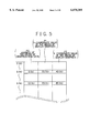
- FIG. 5 is a schematic diagram showing a storage map of the parameter RAM section 22.
- FIG. 6 is a schematic diagram showing a storage map of the graphics ROM section 26.
- FIG. 7 is a timing chart showing timing of display operation, in which ⁇ one screen displaying period ⁇ , ⁇ graphics undisplaying period ⁇ , and ⁇ graphics displaying period ⁇ each of which will be described below, and display timing of each line of the display screen are shown.
- FIG. 8 is a timing chart showing timing of each signal during display operation of the FD-th line of the display screen.
- the graphics in normal display and the graphics in the mesh effect display are treated independently.
- Each graphics data for each graphics is stored in a storage area in the graphics ROM section 26 for storing the graphics data, respectively.
- the normal display and the mesh effect display of the graphics are realized by assigning the respective storage areas of the graphics ROM section 26.
- a display screen G1 is composed of 1 ⁇ m dots (pixels), and is displaying, for example, graphics G2 which is composed of 16 ⁇ 16 pixels all in black levels and graphics G3 which is composed of black level pixels and white level pixels arranged alternately.
- the graphics G2 is realized by displaying graphics ROM data R1 shown in FIG. 6 on the display screen G1, putting the upper left origin (0(h), 0(h)) of the graphics ROM data R1 at coordinates (40(h), F6(h)) of the display screen G1.
- the graphics G3 is realized by displaying graphics ROM data R2 shown in FIG.
- the graphics data 5555(h) (01010101010101) corresponds to a sequence of pixels ⁇ BWBWBWBWBWBWBWBWBWBWBW (B:Black, W:White) ⁇ (The MSB of graphics data corresponds to the right end pixel.)
- the graphics data FFFF(h) (1111111111111111) corresponds to a sequence of pixels ⁇ BBBBBBBBBBBBBB ⁇ .
- graphics ROM data R1 and R2 corresponding to the graphics G2 and G3 respectively are shown on the left side, and graphic images corresponding to the graphics ROM data R1 and R2 respectively are shown on the right side.
- the address of the origin of the graphics ROM data stored in the graphics ROM section 26 (see FIG. 6) is set as a value P0
- the Y-coordinate value of the origin of the display graphics is set as a value P1
- the X-coordinate value of the origin of the display graphics is set as a value P2.
- the above three values P0, P1 and P2 for the graphics G2 are set in an address 5(h) of the parameter RAM section 22
- the above three values P0, P1 and P2 for the graphics G3 are set in an address 9(h) of the parameter RAM section 22.
- the display processing section 2 is supplied with the clock signal S1, the horizontal synchronous signal S2, and the vertical synchronous signal S3, from the unshown system such as a game machine which is using the conventional graphic image display device.
- a term between activation (i.e. a falling edge) of the vertical synchronous signal S3 and activation of the next vertical synchronous signal S3 will be hereafter called ⁇ one screen displaying period ⁇ .
- a term between activation of the vertical synchronous signal S3 and activation of the first horizontal synchronous signal S2 will be hereafter called ⁇ graphics undisplaying period ⁇ .
- a term between the activation of the first horizontal synchronous signal S2 and the activation of the next vertical synchronous signal S3 will be hereafter called ⁇ graphics displaying period ⁇ .
- Parameters for displaying graphics are set in the parameter RAM section 22 during the graphics undisplaying period.
- the scan line count signal S9 counted and outputted by the timing generator section 24 is incremented by one on every activation of the horizontal synchronous signal S2.
- the one screen displaying period is over when the timing generator section 24 is supplied with all the horizontal synchronous signals S2 for the line 0 through the line 1 as shown in FIG. 7.
- FIG. 8 is a timing chart showing detailed timing in display processing for the FD-th line of the display screen G1.
- the timing generator section 24 is initialized according to the supply of the vertical synchronous signal S3 into the display processing section 2.
- the timing generator section 24 counts the number of the supply of the horizontal synchronous signal S2 (falling edge), and the scan line count signal S9 is incremented on every supply (i.e. activation) of the horizontal synchronous signal S2, and eventually, the scan line count signal S9 becomes FD(h).
- the timing generator section 24 is initialized on every supply of the horizontal synchronous signal S2.
- the FIFO section 23 sets the FIFO section emp signal S8 which is supplied to the timing generator section 24 at 1(h) when no data is stored therein, and on storing data, the FIFO section 23 sets the FIFO section emp signal S8 at 0(h), and consequently, output of the FIFO section request signal S7 by the timing generator section 24 is enabled.
- the ROM address is an address in the graphics ROM section 26 where the graphics data of a line of the graphics G2 which should be displayed on the FD-th line of the display screen G1 is stored.
- the timing generator section 24 sends the display start signal S16 to the output section 27.
- the output section 27 increments the line buffer address signal S20 which is supplied to the line buffer section 3 from 40(h) to 4F(h) (see FIG. 3) on every supply of the clock signal S1.
- the line buffer write enable signal S19 which is sent from the output section 27 to the line buffer section 3 is generally set at 1(h), and is set at 0(h) while the line buffer address signal S20 is outputted and incremented.
- the display processing section 2 stores the graphics data of the line of the graphics G2 in the line buffer section 3 as described above.
- the timing generator section 24 sends the FIFO section request signal S7 to the FIFO section 23.
- the timing generator section 24 sends the display start signal S16 to the output section 27 again.
- the output section 27 increments the line buffer address signal S20 which is supplied to the line buffer section 3 from 80(h) to 8F(h) (see FIG. 3) on every supply of the clock signal S1.
- mesh effect display is realized by preparing graphics data for displaying graphics in normal display and graphics data for displaying the graphics in the mesh effect display in the graphics ROM section 26, and treating each graphics data independently.
- FIG. 9 is a block diagram showing composition of a graphic image display device which is proposed by the present inventors, in which the same reference characters as those of FIG. 4 designate the same or corresponding parts to those of FIG. 4 and thus repeated description thereof is omitted for brevity.
- the graphic image display device comprises a display processing section 2A instead of the display processing section 2 of FIG. 4.
- the display processing section 2A includes a mesh pattern generator section 28 and a data mask section 29.
- the mesh pattern generator section 28 is supplied with the scan line count signal S9 from the timing generator section 24, a mesh effect ON/OFF signal S14 from the parameter RAM section 22, and the ROM address signal S15 from the ROM address calculation section 25.
- the mesh pattern generator section 28 generates a mesh pattern according to the supplied scan line count signal S9, the mesh effect ON/OFF signal S14, and the ROM address signal S15, and supplies a mesh signal S21 to the data mask section 29.
- the data mask section 29 executes masking to the graphics data signal S17 read out from the graphics ROM section 26 according to the supplied mesh signal S21, and outputs a processed graphics data signal S23 to the output section 27.
- the display processing section 2A executes masking to the original display graphics data and thereby executes mesh effect display of the display graphics.
- FIG. 10 is a schematic diagram showing a storage map of the parameter RAM section 22 of the graphic image display device.
- a display screen G1 is composed of 1 ⁇ m dots (pixels), and is displaying, for example, graphics G2 which is composed of 16 ⁇ 16 pixels all in black levels and graphics G3 which is composed of black level pixels and white level pixels arranged alternately.
- the graphics G2 is realized by displaying graphics ROM data R1 shown in FIG.
- the graphics G3 is realized by displaying the same original graphics ROM data R1 on the display screen G1, with executing masking operation to the graphics ROM data R1, putting the upper left origin (0(h),0(h)) of the masked graphics ROM data R1 at coordinates (80(h),F0(h)) of the display screen G1.
- the address of the origin of the graphics ROM data stored in the graphics ROM section 26 (see FIG. 11) is set as a value P0
- the Y-coordinate value of the origin of the display graphics is set as a value P1
- the X-coordinate value of the origin of the display graphics is set as a value P2
- ON/OFF information of mesh effect is set as a value P3.
- the above four values P0, P1, P2 and P3 for the graphics G2 are set in an address 3(h) of the parameter RAM section 22, and the above four values P0, P1, P2 and P3 for the graphics G3 are set in an address 7(h) of the parameter RAM section 22.
- the timing generator section 24 in the display processing section 2A is initialized according to supply of the vertical synchronous signal S3 into the display processing section 2A.
- the data I/F section 21 is supplied with the CPU I/F signal S5 from the CPU section 1 during the graphics undisplaying period, identifies the instruction in the CPU I/F signal S5, and outputs the contents of the identified instruction into the parameter RAM section 22 as the parameter RAM write signal S6.
- the timing generator section 24 counts the number of the supply of the horizontal synchronous signal S2 (falling edge), and the scan line count signal S9 is incremented on every supply (i.e. activation) of the horizontal synchronous signal S2, and eventually, the scan line count signal S9 becomes FD(h).
- the timing generator section 24 is initialized on every supply of the horizontal synchronous signal S2.
- the FIFO section 23 sets the FIFO section emp signal S8, which is supplied to the timing generator section 24, at 0(h) according to storage of data, and consequently, output of the FIFO section request signal S7 by the timing generator section 24 is enabled.
- the timing generator section 24 sends the display start signal S16 to the output section 27.
- the output section 27 increments the line buffer address signal S20 which is supplied to the line buffer section 3 from 40(h) to 4F(h) (see FIG. 3) on every supply of the clock signal S1.
- the line buffer write enable signal S19 which is generally set at 1(h), is set at 0(h) while the line buffer address signal S20 is outputted and incremented.
- the output section supplies the line buffer section 3 with the line buffer data signal S18 for the line of the graphics G2, the line buffer write enable signal S19, and the line buffer address signal S20.
- the display processing section 2A stores the graphics data of the line of the graphics G2 in the line buffer section 3 as described above.
- the timing generator section 24 sends the FIFO section request signal S7 to the FIFO section 23.
- the timing generator section 24 sends the display start signal S16 to the output section 27 again.
- the output section 27 increments the line buffer address signal S20 which is supplied to the line buffer section 3 from 80(h) to 8F(h) (see FIG. 3) on every supply of the clock signal S1.
- mesh effect display is realized by preparing original graphics data only, in the graphics ROM section 26, and executing masking to the graphics data according to the mesh signal S21 generated by the mesh pattern generator section 28 according to the mesh effect ON/OFF signal S14, the scan line count signal S9 and the ROM address signal S15. Therefore, in the graphic image display device proposed by the present inventors, preparation of huge amount of graphics data and considerably large capacity of the graphics ROM section 26 are not necessary for executing special effect such as fade-out/fade-in etc. by the mesh effect display.
- a graphic image display device comprising a display processing section and a line buffer section.
- the display processing section is provided with a graphics ROM for storing original graphics data of a plurality of graphic images.
- the display processing section reads original graphics data of a graphic image from the graphics ROM according to a CPU I/F signal supplied from a CPU as graphics processing control information, processes the original graphics data according to the CPU I/F signal, and outputs display graphics data.
- the line buffer section temporarily stores the display graphics data to be displayed on a line of a display screen.
- the display processing section includes a mesh pattern generator means and a line buffer write control means.
- the mesh pattern generator means generates a mesh signal including masking information of a mesh pattern to be given to the display graphics data according to a mesh effect ON/OFF signal which is generated according to instructions in the CPU I/F signal.
- the line buffer write control means controls ON/OFF of writing on the storing of the display graphics data in the line buffer section according to the mesh signal, thereby mesh effect is given to the display graphics data and mesh effect display is realized.
- the line buffer write control means includes a write enable mask section for executing masking to a line buffer write enable signal which enables writing into the line buffer section, according to the value of the mesh signal.
- the display processing section includes a data I/F section, a parameter RAM section, a FIFO section, a timing generator section, a ROM address calculation section, a graphics ROM section, and an output section.
- the data I/F section receives the CPU I/F signal, identifies instructions in the CPU I/F signal, and outputs a FIFO section input signal and a parameter RAM write signal corresponding to each display graphics according to the instructions in the CPU I/F signal.
- the parameter RAM section stores each graphic display parameter according to the parameter RAM write signal, and outputs a ROM origin address signal indicating an address of the origin of the original graphics data of a graphic image stored in the graphics ROM, a X-coordinate origin signal indicating a X-coordinate of the origin of the graphic image to be displayed on the display screen, a Y-coordinate origin signal indicating a Y-coordinate of the origin of the graphic image to be displayed on the display screen, and the mesh effect ON/OFF signal indicating ON/OFF of the mesh effect, according to supply of a FIFO section output signal.
- the FIFO section stores addresses of the parameter RAM section according to the FIFO section input signal, and outputs the FIFO section output signal according to supply of a FIFO section request signal.
- the timing generator section receives a vertical synchronous signal and a horizontal synchronous signal from a system which uses the graphic image display device, counts the number of scan lines, outputs a scan line count signal, generates the FIFO section request signal requesting the FIFO section to output an address of the parameter RAM section, and generates a display start signal.
- the ROM address calculation section calculates a ROM address using the ROM origin address signal, the scan line count signal and the Y-coordinate origin signal, and outputs a ROM address signal.
- the graphics ROM section provided with the graphics ROM outputs a graphics data signal according to the ROM address signal.
- the output section receives the graphics data signal and the X-coordinate origin signal, and outputs a line buffer data signal, a line buffer write enable signal, and a line buffer address signal, according to supply of a clock signal from the system using the graphic image display device and the display start signal.
- the parameter RAM section stores ROM origin address information corresponding to the ROM origin address signal, X-coordinate origin information corresponding to the X-coordinate origin signal, Y-coordinate origin information corresponding to the Y-coordinate origin signal, and mesh effect ON/OFF information corresponding to the mesh effect ON/OFF signal, as the graphic display parameters, and graphics data of a graphic image stored in an address of the graphics ROM indicated by the ROM origin address signal is displayed on the display screen putting the origin of the graphic image on coordinates of the display screen indicated by the X-coordinate origin signal and the Y-coordinate origin signal, in which normal display of the graphic image is executed according to the first value of the mesh effect ON/OFF signal and mesh effect display of the graphic image is executed according to the second value of the mesh effect ON/OFF signal.
- a method for displaying graphic images comprising the following basic steps.
- original graphics data of a graphic image is read from a graphics ROM in a display processing section which stores original graphics data of a plurality of graphic images, according to a CPU I/F signal supplied from a CPU as graphics processing control information.
- the original graphics data is processed according to the CPU I/F signal and display graphics data is generated.
- the display graphics data is outputted from the display processing section to a line buffer section for temporarily storing the display graphics data to be displayed on a line of a display screen.
- the display graphics data is temporarily stored in the line buffer section.
- the display graphics data is displayed on the line of the display screen.
- the method further includes the following steps.
- In the first step it is judged whether or not instruction to execute mesh effect display is included in the CPU I/F signal and a mesh effect ON/OFF signal is generated.
- a mesh signal including masking information of a mesh pattern to be given to the display graphics data is generated according to the mesh effect ON/OFF signal.
- ON/OFF of writing on the storing of the display graphics data in the line buffer section is controlled according to the mesh signal, and thereby mesh effect is given to the display graphics data and mesh effect display is realized.
- the control of the ON/OFF of the writing is realized by executing masking to a line buffer write enable signal for enabling writing into the line buffer section, according to the value of the mesh signal.
- FIG. 1 is a schematic diagram showing examples of mesh effects
- FIG. 2 is a schematic diagram showing an example of functions of mesh effect display
- FIG. 3 is a schematic diagram showing an example of a graphic image display
- FIG. 4 is a block diagram showing composition of a general conventional graphic image display device
- FIG. 5 is a schematic diagram showing a storage map of a parameter RAM section of the graphic image display device of FIG. 4;
- FIG. 6 is a schematic diagram showing a storage map of a graphics ROM section of the graphic image display device of FIG. 4;
- FIG. 7 is a timing chart showing timing of display operation of the graphic image display device of FIG. 4;
- FIG. 8 is a timing chart showing timing of each signal in the graphic image display device of FIG. 4 during display operation of the FD-th line of the display screen;
- FIG. 9 is a block diagram showing composition of a graphic image display device which is proposed by the present inventors.
- FIG. 10 is a schematic diagram showing a storage map of a parameter RAM section 22 of the graphic image display device of FIG. 9;
- FIG. 11 is a schematic diagram showing a storage map of a graphics ROM section of the graphic image display device of FIG. 9;
- FIG. 12 is a timing chart showing timing of each signal in the graphic image display device of FIG. 9 during display operation of the FD-th line of the display screen;
- FIG. 13 is a block diagram showing composition of a graphic image display device according to an embodiment of the present invention.
- FIG. 14 is a timing chart showing timing of each signal in the graphic image display device of FIG. 13 during display operation of the FD-th line of the display screen;
- FIG. 15 is a flow chart showing the operation of the graphic image display device according to an embodiment of the present invention.
- FIG. 16 is a flow chart showing steps in the graphics display processing in FIG. 15;
- FIG. 17 is a schematic diagram showing an example of a transitional graphic image display executed by the graphic image display device of FIG. 13;
- FIG. 18 is a schematic diagram showing a storage map of a graphics ROM section of the graphic image display device of FIG. 13 for executing the transitional graphic image display of FIG. 17;
- FIG. 19 is a schematic diagram showing a storage map of a parameter RAM section of the graphic image display device of FIG. 9 when the transitional graphic image display of FIG. 17 is executed.
- FIG. 13 is a block diagram showing composition of the graphic image display device according to an embodiment of the present invention, in which the same reference characters as those of FIG. 9 designate the same or corresponding parts to those of FIG. 9.
- the graphic image display device is installed in or connected to an unshown system such as a game machine which uses the graphic image display device, and a CPU section 1 of the system sends a CPU I/F signal S5 including processing information for displaying graphics to the graphic image display device.
- the graphic image display device comprises a display processing section 2B for executing display processing according to the CPU I/F signal S5 and outputting graphic display data, and a line buffer section 3 for temporarily storing the graphic display data to be displayed on a line of the display screen.
- the display processing section 2B is different from the display processing section 2A in the graphic image display device of FIG. 9.
- the display processing section 2B includes a data I/F section 21, a parameter RAM section 22, a FIFO section 23, a timing generator section 24, a ROM address calculation section 25, a graphics ROM section 26, and an output section 27, in the same way as the display processing section 2A of the graphic image display device of FIG. 9.
- the display processing section 2B further includes a mesh pattern generator section 28B and a write enable mask section 30.
- the data I/F section 21 receives the CPU I/F signal S5 from the CPU section 1, and outputs a FIFO section input signal S4 and a parameter RAM write signal S6 corresponding to each display graphics, according to the received CPU I/F signal S5.
- the parameter RAM section 22 receives the parameter RAM write signal S6 from the data I/F section 21, and stores each graphic display parameter according to the received parameter RAM write signal S6.
- the parameter RAM section 22 receives a FIFO section output signal SlO from the FIFO section 23. and outputs a ROM origin address signal S11, a Y-coordinate origin signal S12, a X-coordinate origin signal S13, and a mesh effect ON/OFF signal S14 according to the received FIFO section output signal S10.
- the FIFO section 23 receives the FIFO section input signal S4 from the data I/F section 21, and stores addresses of the parameter RAM section 22 according to the received FIFO section input signal S4.
- the FIFO section 23 receives a FIFO section request signal S7 from the timing generator section 24, and outputs the FIFO section output signal S10 according to the reception of the FIFO section request signal S7, and outputs a FIFO section emp signal S8 after the output of the FIFO section output signal S10.
- the timing generator section 24 receives a vertical synchronous signal S3 and a horizontal synchronous signal S2 from an unshown system such as a game machine which is using the graphic image display device, counts the number of scan lines, and outputs a scan line count signal S9.
- the timing generator section 24 also outputs the FIFO section request signal S7 and a display start signal S16.
- the ROM address calculation section 25 receives the ROM origin address signal S11 and the Y-coordinate origin signal S12 from the parameter RAM section 22 and the scan line count signal S9 from the timing generator section 24, calculates a ROM address according to the signals, and outputs a ROM address signal S15.
- the graphics ROM section 26 receives the ROM address signal S15 from the ROM address calculation section 25, and outputs a graphics data signal S17 according to the received ROM address signal S15.
- the output section 27 receives a clock signal S1 from the unshown system which is using the graphic image display device, and receives the display start signal S16 from the timing generator section 24.
- the output section 27 receives the graphics data signal S17 and the X-coordinate origin signal S13, and outputs a line buffer data signal S18, a line buffer write enable signal S19, and a line buffer address signal S20, according to the reception of the clock signal S1 and the display start signal S16.
- the mesh pattern generator section 28B is supplied with the scan line count signal S9, the mesh effect ON/OFF signal S14 and the ROM address signal S15, generates a mesh signal 21 according to the supplied signals, and outputs each bit of the mesh signal 21 synchronized with the clock signal S1.
- the write enable mask section 30 executes masking to the line buffer write enable signal S19 supplied from the output section 27 according to the supplied mesh signal S21, and outputs a masked line buffer write enable signal S22.
- the display processing section 2B executes mesh effect display by executing masking to the line buffer write enable signal S19 on storing of the graphics data into the line buffer 3.
- FIG. 3, FIG. 11 and FIG. 10 are common to the device of FIG. 9 and the device of this embodiment.
- the display screen G1 is composed of 1 ⁇ m dots (pixels), and is displaying, for example, graphics G2 which is composed of 16 ⁇ 16 pixels all in black levels and graphics G3 which is composed of black level pixels and white level pixels arranged alternately.
- the graphics G2 is realized by displaying graphics ROM data R1 shown in FIG. 11 on the display screen G1, putting the upper left origin (0(h),0(h)) of the graphics ROM data R1 at coordinates (40(h),F6(h)) of the display screen G1.
- the graphics G3 is realized by displaying the same original graphics ROM data R1 on the display screen G1, with executing masking operation to the graphics ROM data R1 by masking the line buffer write enable signal Sl9, putting the upper left origin (0(h),0(h)) of the masked graphics ROM data R1 at coordinates (80(h),F0(h)) of the display screen G1.
- the address of the origin of the graphics ROM data stored in the graphics ROM section 26 (see FIG. 11) is set as a value P0
- the Y-coordinate value of the origin of the display graphics is set as a value P1
- the X-coordinate value of the origin of the display graphics is set as a value P2
- ON/OFF information of mesh effect is set as a value P3.
- the above four values P0, P1, P2 and P3 for the graphics G2 are set in an address 3(h) of the parameter RAM section 22.
- the above four values P0, P1, P2 and P3 for the graphics G3 are set in an address 7(h) of the parameter RAM section 22.
- the timing generator section 24 in the display processing section 2B is initialized according to supply of the vertical synchronous signal S3 to the display processing section 2B (step P1, P2).
- the data I/F section 21 is supplied with the CPU 1/F signal S5 from the CPU section 1 during the graphics undisplaying period shown in FIG. 7, identifies the instruction in the CPU I/F signal S5, and outputs the contents of the identified instruction into the parameter RAM section 22 as the parameter RAM write signal S6.
- step P4 graphics display processing
- the timing generator section 24 counts the number of the supply of the horizontal synchronous signal S2 (falling edge), and the scan line count signal S9 is incremented on every supply (i.e. activation) of the horizontal synchronous signal S2 (step P41), and eventually, the scan line count signal S9 becomes FD(h).
- the timing generator section 24 is initialized on every supply of the horizontal synchronous signal S2 (step S42).
- the FIFO section 23 sets the FIFO section emp signal S8, which is supplied to the timing generator section 24, at 0(h) according to storage of data, and consequently, output of the FIFO section request signal S7 by the timing generator section 24 is enabled.
- the timing generator section 24 sends the display start signal S16 to the output section 27.
- the output section 27 increments the line buffer address signal S20 which is supplied to the line buffer section 3 from 40(h) to 4F(h) (see FIG. 3) on every supply of the clock signal S1.
- the line buffer write enable signal S19 which is generally set at 1(h), is set at 0(h) while the line buffer address signal S20 is outputted and incremented.
- the write enable mask section 30 executes no masking to the line buffer write enable signal S19 supplied from the output section 27, and supplies the line buffer write enable signal S19 into the line buffer section 3 as the masked line buffer write enable signal S22.
- the display processing section 2B stores the graphics data of the line of the graphics G2 in the line buffer section 3 as described above.
- the timing generator section 24 sends the FIFO section request signal S7 to the FIFO section 23.
- the timing generator section 24 sends the display start signal S16 to the output section 27 again.
- the output section 27 increments the line buffer address signal S20 which is supplied to the line,e buffer section 3 from 80(h) to 8F(h) (see FIG. 3) on every supply of the clock signal S1.
- the line buffer write enable signal S19 which is generally set at 1(h), is set at 0(h) while the line buffer address signal S20 is outputted and incremented.
- the write enable mask section 30 executes masking to the line buffer write enable signal S19 according to each bit of the mesh signal S21 and generates the masked line buffer write enable signal S22, and supplies the signal S22 to the line buffer section 3. Writing into the line buffer section 3 is executed only when the masked line buffed write enable signal S22 is in a low level (step P51).
- step P4 The above graphics display processing is executed until the last line of the display screen is displayed (step P4, P5, P6), and process is returned to the step P1 for displaying the next display screen.
- ON/OFF of writing of each bit of graphics data into the line buffer section 3 can be controlled by executing masking to the line buffer write enable signal S19 according to the mesh signal 21 generated by the mesh pattern generator section 28B.
- the graphic image display device it is possible to execute overlapping display of mesh effect graphics.
- the letter ⁇ B ⁇ graphics G4 gradually goes out via graphics G5 (mesh effect display of the letter ⁇ B ⁇ ) (fade-out)
- the letter ⁇ A ⁇ graphics G7
- FIG. 17 is a schematic diagram showing an example of a transitional graphic image display
- FIG. 18 is a schematic diagram showing a storage map of the graphics ROM section 26.
- the display screen G1 composed of 1 ⁇ m dots (pixels) is displaying, for example, graphics G3 which is composed of black level pixels and white level pixels arranged alternately and graphics G7 (the letter ⁇ A ⁇ shown in FIG. 2) together (transitional display).
- the graphics G3 is realized by displaying the graphics ROM data R1 on the display screen G1, with executing masking operation to the graphics ROM data R1 by masking the line buffer write enable signal S19, putting the upper left origin (0(h),0(h)) of the masked graphics ROM data R1 at coordinates (80(h),F0(h)) of the display screen G1.
- the graphics G7 is realized by displaying graphics ROM data R7 shown in FIG. 18 on the display screen G1, putting the upper left origin (0(h),0(h)) of the graphics ROM data R7 at coordinates (80(h),F0(h)) of the display screen G1.
- FIG. 19 which is showing the storage map of the parameter RAM section 22, in order to execute transitional display on the display screen G1 as shown in FIG. 17, the address of the origin of the graphics ROM data stored in the graphics ROM section 26 (see FIG. 8) is set as a value P0, the Y-coordinate value of the origin of the display graphics is set as a value P1, the X-coordinate value of the origin of the display graphics is set as a value P2, and ON/OFF information of mesh effect is set as a value P3.
- the above four values P0, P1, P2 and P3 for the graphics G7 are set in an address 3(h) of the parameter RAM section 22, and the above four values P0, P1, P2 and P3 for the graphics G3 are set in an address 7(h) of the parameter RAM section 22.
- the timing generator section 24 in the display processing section 2B is initialized according to supply of the vertical synchronous signal S3 to the display processing section 2B (step P1, P2).
- the data I/F section 21 is supplied with the CPU I/F signal S5 from the CPU section 1 during the graphics undisplaying period shown in FIG. 7, identifies the instruction in the CPU I/F signal S5, and outputs the contents of the identified instruction into the parameter RAM section 22 as the parameter RAM write signal S6.
- step P4 graphics display processing
- the timing generator section 24 counts the number of the supply of the horizontal synchronous signal S2 (falling edge), and the scan line count signal S9 is incremented on every supply of the horizontal synchronous signal S2 (step P41), and eventually, the scan line count signal S9 becomes FD(h).
- the timing generator section 24 is initialized on every supply of the horizontal synchronous signal S2 (step S42).
- the FIFO section 23 sets the FIFO section emp signal S8 at 0(h) according to storage of data, and consequently, output of the FIFO section request signal S7 by the timing generator section 24 is enabled.
- the ROM address is an address in the graphics ROM section 26 where the graphics data of a line of the graphics G7 which should be displayed on the FD-th line of the display screen G1 is stored (step P46).
- the timing generator section 24 sends the display start signal S16 to the output section 27.
- the output section 27 increments the line buffer address signal S20 which is supplied to the line buffer section 3 from 80(h) to 8F(h) (see FIG. 17) on every supply of the clock signal S1.
- the line buffer write enable signal S19 which is generally set at 1(h), is set at 0(h) while the line buffer address signal S20 is outputted and incremented.
- the write enable mask section 30 executes no masking to the line buffer write enable signal S19 supplied from the output section 27, and supplies the line buffer write enable signal S19 into the line buffer section 3 as the masked line buffer write enable signal S22.
- the display processing section 2B stores the graphics data of the line of the graphics G7 in the line buffer section 3 as described above.
- the timing generator section 24 sends the display start signal S16 to the output section 27 again.
- the output section 27 increments the line buffer address signal S20 which is supplied to the line buffer section 3 from 80(h) to 8F(h) (see FIG. 17) on every supply of the clock signal S1.
- the line buffer write enable signal S19 which is generally set at 1(h), is set at 0(h) while the line buffer address signal S20 is outputted and incremented.
- the write enable mask section 30 executes masking to the line buffer write enable signal S19 according to each bit of the mesh signal S21 and generates the masked line buffer write enable signal S22, and supplies the signal S22 to the line buffer section 3. Writing into the line buffer section 3 is executed only when the masked line buffer write enable signal S22 is in a low level (step P51).
- the display processing section 2B stores the graphics data of the line of the graphics G3 in the line buffer section 3 which has been storing the graphics data of the line of the graphics G7, as described above.
- step P4 The above graphics display processing is executed until the last line of the display screen is displayed (step P4, P5, P6), and process is returned to the step P1 for displaying the next display screen.
- overlapping display of mesh effect graphics can be executed and transition of display graphics can be executed smoothly, without preparation of huge amount of graphics data or large capacity of the graphics ROM section 26.
- transitional display various kinds of transitional displays can be executed according to the embodiment.
- graphics Gb is replaced with graphics Ga (fade-out/fade-in)
- various kinds of transitional displays and variations are possible according to the embodiment as follows:
- the mesh pattern generated by the mesh pattern generator section 28B is not limited to the checker pattern shown in FIG. 17. Various types of mesh patterns such as patterns shown in FIG. 1. are possible. It is also possible to let the mesh pattern generator section 28B generate a plurality of mesh patterns and switch mesh patterns according to instruction in the CPU I/F signal S5.
Landscapes
- Engineering & Computer Science (AREA)
- Physics & Mathematics (AREA)
- Computer Hardware Design (AREA)
- General Physics & Mathematics (AREA)
- Theoretical Computer Science (AREA)
- Radar, Positioning & Navigation (AREA)
- Remote Sensing (AREA)
- Controls And Circuits For Display Device (AREA)
- Digital Computer Display Output (AREA)
- Processing Or Creating Images (AREA)
Applications Claiming Priority (2)
| Application Number | Priority Date | Filing Date | Title |
|---|---|---|---|
| JP8296321A JP3037161B2 (ja) | 1996-11-08 | 1996-11-08 | 図形画像表示装置及び図形画像表示方法 |
| JP8-296321 | 1996-11-08 |
Publications (1)
| Publication Number | Publication Date |
|---|---|
| US6078305A true US6078305A (en) | 2000-06-20 |
Family
ID=17832038
Family Applications (1)
| Application Number | Title | Priority Date | Filing Date |
|---|---|---|---|
| US08/965,368 Expired - Fee Related US6078305A (en) | 1996-11-08 | 1997-11-06 | Device and method displaying a mesh effect with line buffer |
Country Status (5)
| Country | Link |
|---|---|
| US (1) | US6078305A (fr) |
| EP (1) | EP0841651A3 (fr) |
| JP (1) | JP3037161B2 (fr) |
| KR (1) | KR100263580B1 (fr) |
| TW (1) | TW350948B (fr) |
Cited By (19)
| Publication number | Priority date | Publication date | Assignee | Title |
|---|---|---|---|---|
| US6364770B1 (en) * | 1998-10-08 | 2002-04-02 | Konami Co., Ltd. | Image creating apparatus, displayed scene switching method for the image creating apparatus, computer-readable recording medium containing displayed scene switching program for the image creating apparatus, and video game machine |
| US20020106018A1 (en) * | 2001-02-05 | 2002-08-08 | D'luna Lionel | Single chip set-top box system |
| US20020167535A1 (en) * | 2001-05-14 | 2002-11-14 | Konami Corporation | Image forming method, computer program for forming image, and image forming apparatus |
| US6529935B1 (en) | 1998-11-09 | 2003-03-04 | Broadcom Corporation | Graphics display system with unified memory architecture |
| US6538656B1 (en) | 1999-11-09 | 2003-03-25 | Broadcom Corporation | Video and graphics system with a data transport processor |
| US6573905B1 (en) | 1999-11-09 | 2003-06-03 | Broadcom Corporation | Video and graphics system with parallel processing of graphics windows |
| US6636222B1 (en) | 1999-11-09 | 2003-10-21 | Broadcom Corporation | Video and graphics system with an MPEG video decoder for concurrent multi-row decoding |
| US6661422B1 (en) | 1998-11-09 | 2003-12-09 | Broadcom Corporation | Video and graphics system with MPEG specific data transfer commands |
| US20040028141A1 (en) * | 1999-11-09 | 2004-02-12 | Vivian Hsiun | Video decoding system having a programmable variable-length decoder |
| US6768774B1 (en) | 1998-11-09 | 2004-07-27 | Broadcom Corporation | Video and graphics system with video scaling |
| US6798420B1 (en) | 1998-11-09 | 2004-09-28 | Broadcom Corporation | Video and graphics system with a single-port RAM |
| US6853385B1 (en) | 1999-11-09 | 2005-02-08 | Broadcom Corporation | Video, audio and graphics decode, composite and display system |
| US6975324B1 (en) | 1999-11-09 | 2005-12-13 | Broadcom Corporation | Video and graphics system with a video transport processor |
| US20070030276A1 (en) * | 1998-11-09 | 2007-02-08 | Macinnis Alexander G | Video and graphics system with parallel processing of graphics windows |
| US20070120874A1 (en) * | 2003-04-25 | 2007-05-31 | Macinnis Alexander G | Graphics display system with line buffer control scheme |
| US20070165787A1 (en) * | 2005-12-24 | 2007-07-19 | Samsung Electronics Co., Ltd. | Apparatus and method for controlling home network devices |
| US7738768B1 (en) | 2005-12-16 | 2010-06-15 | The Directv Group, Inc. | Method and apparatus for increasing the quality of service for digital video services for mobile reception |
| US8063916B2 (en) | 2003-10-22 | 2011-11-22 | Broadcom Corporation | Graphics layer reduction for video composition |
| US8199154B2 (en) | 1998-11-09 | 2012-06-12 | Broadcom Corporation | Low resolution graphics mode support using window descriptors |
Citations (14)
| Publication number | Priority date | Publication date | Assignee | Title |
|---|---|---|---|---|
| JPS4856032A (fr) * | 1971-11-13 | 1973-08-07 | ||
| US4360831A (en) * | 1979-11-16 | 1982-11-23 | Quantel Limited | Multiple image digital processing system |
| US4398189A (en) * | 1981-08-20 | 1983-08-09 | Bally Manufacturing Corporation | Line buffer system for displaying multiple images in a video game |
| US4531120A (en) * | 1983-01-20 | 1985-07-23 | International Business Machines Corporation | Superposing graphic patterns |
| EP0199272A2 (fr) * | 1985-04-16 | 1986-10-29 | Wang Laboratories Inc. | Visualisation monochromatique d'images en couleurs |
| US4645459A (en) * | 1982-07-30 | 1987-02-24 | Honeywell Inc. | Computer generated synthesized imagery |
| JPS6361372A (ja) * | 1986-09-01 | 1988-03-17 | Nec Corp | 図形表示装置 |
| US4843568A (en) * | 1986-04-11 | 1989-06-27 | Krueger Myron W | Real time perception of and response to the actions of an unencumbered participant/user |
| US4868557A (en) * | 1986-06-04 | 1989-09-19 | Apple Computer, Inc. | Video display apparatus |
| US5043714A (en) * | 1986-06-04 | 1991-08-27 | Apple Computer, Inc. | Video display apparatus |
| US5386505A (en) * | 1990-11-15 | 1995-01-31 | International Business Machines Corporation | Selective control of window related overlays and underlays |
| US5481653A (en) * | 1989-07-26 | 1996-01-02 | Canon Kabushiki Kaisha | Digital image processing apparatus for synthesizing an image form at least two images |
| US5611027A (en) * | 1992-08-04 | 1997-03-11 | International Business Machines Corporation | Image enhancement with mask having fuzzy edges |
| US5847713A (en) * | 1989-12-28 | 1998-12-08 | Canon Kabushiki Kaisha | Output apparatus with size change of character patterns only |
-
1996
- 1996-11-08 JP JP8296321A patent/JP3037161B2/ja not_active Expired - Fee Related
-
1997
- 1997-11-05 EP EP97119352A patent/EP0841651A3/fr not_active Withdrawn
- 1997-11-06 US US08/965,368 patent/US6078305A/en not_active Expired - Fee Related
- 1997-11-08 KR KR1019970058940A patent/KR100263580B1/ko not_active Expired - Fee Related
- 1997-11-08 TW TW086116692A patent/TW350948B/zh active
Patent Citations (16)
| Publication number | Priority date | Publication date | Assignee | Title |
|---|---|---|---|---|
| JPS4856032A (fr) * | 1971-11-13 | 1973-08-07 | ||
| US4360831A (en) * | 1979-11-16 | 1982-11-23 | Quantel Limited | Multiple image digital processing system |
| US4398189A (en) * | 1981-08-20 | 1983-08-09 | Bally Manufacturing Corporation | Line buffer system for displaying multiple images in a video game |
| US4645459A (en) * | 1982-07-30 | 1987-02-24 | Honeywell Inc. | Computer generated synthesized imagery |
| US4531120A (en) * | 1983-01-20 | 1985-07-23 | International Business Machines Corporation | Superposing graphic patterns |
| US4703318A (en) * | 1984-03-30 | 1987-10-27 | Wang Laboratories, Inc. | Character-based monochromatic representation of color images |
| EP0199272A2 (fr) * | 1985-04-16 | 1986-10-29 | Wang Laboratories Inc. | Visualisation monochromatique d'images en couleurs |
| US4843568A (en) * | 1986-04-11 | 1989-06-27 | Krueger Myron W | Real time perception of and response to the actions of an unencumbered participant/user |
| US4868557A (en) * | 1986-06-04 | 1989-09-19 | Apple Computer, Inc. | Video display apparatus |
| GB2226938A (en) * | 1986-06-04 | 1990-07-11 | Apple Computer | Video display apparatus |
| US5043714A (en) * | 1986-06-04 | 1991-08-27 | Apple Computer, Inc. | Video display apparatus |
| JPS6361372A (ja) * | 1986-09-01 | 1988-03-17 | Nec Corp | 図形表示装置 |
| US5481653A (en) * | 1989-07-26 | 1996-01-02 | Canon Kabushiki Kaisha | Digital image processing apparatus for synthesizing an image form at least two images |
| US5847713A (en) * | 1989-12-28 | 1998-12-08 | Canon Kabushiki Kaisha | Output apparatus with size change of character patterns only |
| US5386505A (en) * | 1990-11-15 | 1995-01-31 | International Business Machines Corporation | Selective control of window related overlays and underlays |
| US5611027A (en) * | 1992-08-04 | 1997-03-11 | International Business Machines Corporation | Image enhancement with mask having fuzzy edges |
Non-Patent Citations (2)
| Title |
|---|
| Foley et al., "Computer Graphics: Principles and Practice", Addison-Wesley Publishing Co., pp. 835-839, Nov. 1993. |
| Foley et al., Computer Graphics: Principles and Practice , Addison Wesley Publishing Co., pp. 835 839, Nov. 1993. * |
Cited By (77)
| Publication number | Priority date | Publication date | Assignee | Title |
|---|---|---|---|---|
| US6364770B1 (en) * | 1998-10-08 | 2002-04-02 | Konami Co., Ltd. | Image creating apparatus, displayed scene switching method for the image creating apparatus, computer-readable recording medium containing displayed scene switching program for the image creating apparatus, and video game machine |
| US7184058B2 (en) | 1998-11-09 | 2007-02-27 | Broadcom Corporation | Graphics display system with anti-aliased text and graphics feature |
| US7446774B1 (en) | 1998-11-09 | 2008-11-04 | Broadcom Corporation | Video and graphics system with an integrated system bridge controller |
| US6529935B1 (en) | 1998-11-09 | 2003-03-04 | Broadcom Corporation | Graphics display system with unified memory architecture |
| US9575665B2 (en) | 1998-11-09 | 2017-02-21 | Broadcom Corporation | Graphics display system with unified memory architecture |
| US6570579B1 (en) | 1998-11-09 | 2003-05-27 | Broadcom Corporation | Graphics display system |
| US9111369B2 (en) | 1998-11-09 | 2015-08-18 | Broadcom Corporation | Graphics accelerator |
| US6608630B1 (en) * | 1998-11-09 | 2003-08-19 | Broadcom Corporation | Graphics display system with line buffer control scheme |
| US6630945B1 (en) | 1998-11-09 | 2003-10-07 | Broadcom Corporation | Graphics display system with graphics window control mechanism |
| US9077997B2 (en) | 1998-11-09 | 2015-07-07 | Broadcom Corporation | Graphics display system with unified memory architecture |
| US6661427B1 (en) | 1998-11-09 | 2003-12-09 | Broadcom Corporation | Graphics display system with video scaler |
| US6661422B1 (en) | 1998-11-09 | 2003-12-09 | Broadcom Corporation | Video and graphics system with MPEG specific data transfer commands |
| US8848792B2 (en) | 1998-11-09 | 2014-09-30 | Broadcom Corporation | Video and graphics system with video scaling |
| US8493415B2 (en) | 1998-11-09 | 2013-07-23 | Broadcom Corporation | Graphics display system with video scaler |
| US6721837B2 (en) | 1998-11-09 | 2004-04-13 | Broadcom Corporation | Graphics display system with unified memory architecture |
| US6731295B1 (en) | 1998-11-09 | 2004-05-04 | Broadcom Corporation | Graphics display system with window descriptors |
| US6738072B1 (en) | 1998-11-09 | 2004-05-18 | Broadcom Corporation | Graphics display system with anti-flutter filtering and vertical scaling feature |
| US6744472B1 (en) | 1998-11-09 | 2004-06-01 | Broadcom Corporation | Graphics display system with video synchronization feature |
| US6768774B1 (en) | 1998-11-09 | 2004-07-27 | Broadcom Corporation | Video and graphics system with video scaling |
| US20040150652A1 (en) * | 1998-11-09 | 2004-08-05 | Broadcom Corporation | Graphics display system with window descriptors |
| US8390635B2 (en) | 1998-11-09 | 2013-03-05 | Broadcom Corporation | Graphics accelerator |
| US6798420B1 (en) | 1998-11-09 | 2004-09-28 | Broadcom Corporation | Video and graphics system with a single-port RAM |
| US6819330B2 (en) | 1998-11-09 | 2004-11-16 | Broadcom Corporation | Graphics display System with color look-up table loading mechanism |
| US20040246257A1 (en) * | 1998-11-09 | 2004-12-09 | Macinnis Alexander G. | Graphics accelerator |
| US8199154B2 (en) | 1998-11-09 | 2012-06-12 | Broadcom Corporation | Low resolution graphics mode support using window descriptors |
| US20110193868A1 (en) * | 1998-11-09 | 2011-08-11 | Broadcom Corporation | Graphics accelerator |
| US7991049B2 (en) | 1998-11-09 | 2011-08-02 | Broadcom Corporation | Video and graphics system with video scaling |
| US7920151B2 (en) | 1998-11-09 | 2011-04-05 | Broadcom Corporation | Graphics display system with video scaler |
| US6879330B2 (en) | 1998-11-09 | 2005-04-12 | Broadcom Corporation | Graphics display system with anti-flutter filtering and vertical scaling feature |
| US6927783B1 (en) | 1998-11-09 | 2005-08-09 | Broadcom Corporation | Graphics display system with anti-aliased text and graphics feature |
| US7911483B1 (en) | 1998-11-09 | 2011-03-22 | Broadcom Corporation | Graphics display system with window soft horizontal scrolling mechanism |
| US7002602B2 (en) | 1998-11-09 | 2006-02-21 | Broadcom Corporation | Apparatus and method for blending graphics and video surfaces |
| US7015928B2 (en) | 1998-11-09 | 2006-03-21 | Broadcom Corporation | Graphics display system with color look-up table loading mechanism |
| US7057622B2 (en) | 1998-11-09 | 2006-06-06 | Broadcom Corporation | Graphics display system with line buffer control scheme |
| US7071944B2 (en) | 1998-11-09 | 2006-07-04 | Broadcom Corporation | Video and graphics system with parallel processing of graphics windows |
| US7098930B2 (en) | 1998-11-09 | 2006-08-29 | Broadcom Corporation | Graphics display system with anti-flutter filtering and vertical scaling feature |
| US7110006B2 (en) | 1998-11-09 | 2006-09-19 | Broadcom Corporation | Video, audio and graphics decode, composite and display system |
| US6700588B1 (en) | 1998-11-09 | 2004-03-02 | Broadcom Corporation | Apparatus and method for blending graphics and video surfaces |
| US7746354B2 (en) | 1998-11-09 | 2010-06-29 | Broadcom Corporation | Graphics display system with anti-aliased text and graphics feature |
| US7554562B2 (en) | 1998-11-09 | 2009-06-30 | Broadcom Corporation | Graphics display system with anti-flutter filtering and vertical scaling feature |
| US7659900B2 (en) | 1998-11-09 | 2010-02-09 | Broadcom Corporation | Video and graphics system with parallel processing of graphics windows |
| US7227582B2 (en) | 1998-11-09 | 2007-06-05 | Broadcom Corporation | Graphics display system with video synchronization feature |
| US7598962B2 (en) | 1998-11-09 | 2009-10-06 | Broadcom Corporation | Graphics display system with window descriptors |
| US7256790B2 (en) | 1998-11-09 | 2007-08-14 | Broadcom Corporation | Video and graphics system with MPEG specific data transfer commands |
| US7277099B2 (en) | 1998-11-09 | 2007-10-02 | Broadcom Corporation | Video and graphics system with an MPEG video decoder for concurrent multi-row decoding |
| US20070285440A1 (en) * | 1998-11-09 | 2007-12-13 | Macinnis Alexander G | Graphics display system with video synchronization feature |
| US7310104B2 (en) | 1998-11-09 | 2007-12-18 | Broadcom Corporation | Graphics display system with anti-flutter filtering and vertical scaling feature |
| US7365752B2 (en) | 1998-11-09 | 2008-04-29 | Broadcom Corporation | Video and graphics system with a single-port RAM |
| US20070030276A1 (en) * | 1998-11-09 | 2007-02-08 | Macinnis Alexander G | Video and graphics system with parallel processing of graphics windows |
| US7530027B2 (en) | 1998-11-09 | 2009-05-05 | Broadcom Corporation | Graphics display system with graphics window control mechanism |
| US7538783B2 (en) | 1998-11-09 | 2009-05-26 | Broadcom Corporation | Graphics display system with video scaler |
| US7545438B2 (en) | 1998-11-09 | 2009-06-09 | Broadcom Corporation | Graphics display system with video synchronization feature |
| US7554553B2 (en) | 1998-11-09 | 2009-06-30 | Broadcom Corporation | Graphics display system with anti-flutter filtering and vertical scaling feature |
| US8913667B2 (en) | 1999-11-09 | 2014-12-16 | Broadcom Corporation | Video decoding system having a programmable variable-length decoder |
| US6853385B1 (en) | 1999-11-09 | 2005-02-08 | Broadcom Corporation | Video, audio and graphics decode, composite and display system |
| US6538656B1 (en) | 1999-11-09 | 2003-03-25 | Broadcom Corporation | Video and graphics system with a data transport processor |
| US6636222B1 (en) | 1999-11-09 | 2003-10-21 | Broadcom Corporation | Video and graphics system with an MPEG video decoder for concurrent multi-row decoding |
| US7667715B2 (en) | 1999-11-09 | 2010-02-23 | Broadcom Corporation | Video, audio and graphics decode, composite and display system |
| US20040028141A1 (en) * | 1999-11-09 | 2004-02-12 | Vivian Hsiun | Video decoding system having a programmable variable-length decoder |
| US20050044175A1 (en) * | 1999-11-09 | 2005-02-24 | Francis Cheung | Transport processor |
| US7848430B2 (en) | 1999-11-09 | 2010-12-07 | Broadcom Corporation | Video and graphics system with an MPEG video decoder for concurrent multi-row decoding |
| US6975324B1 (en) | 1999-11-09 | 2005-12-13 | Broadcom Corporation | Video and graphics system with a video transport processor |
| US6870538B2 (en) | 1999-11-09 | 2005-03-22 | Broadcom Corporation | Video and graphics system with parallel processing of graphics windows |
| US6573905B1 (en) | 1999-11-09 | 2003-06-03 | Broadcom Corporation | Video and graphics system with parallel processing of graphics windows |
| US20060268012A1 (en) * | 1999-11-09 | 2006-11-30 | Macinnis Alexander G | Video, audio and graphics decode, composite and display system |
| US6781601B2 (en) | 1999-11-09 | 2004-08-24 | Broadcom Corporation | Transport processor |
| US20020106018A1 (en) * | 2001-02-05 | 2002-08-08 | D'luna Lionel | Single chip set-top box system |
| US9668011B2 (en) | 2001-02-05 | 2017-05-30 | Avago Technologies General Ip (Singapore) Pte. Ltd. | Single chip set-top box system |
| US20020167535A1 (en) * | 2001-05-14 | 2002-11-14 | Konami Corporation | Image forming method, computer program for forming image, and image forming apparatus |
| US6833841B2 (en) * | 2001-05-14 | 2004-12-21 | Konami Corporation | Image forming method, computer program for forming image, and image forming apparatus |
| US7667710B2 (en) | 2003-04-25 | 2010-02-23 | Broadcom Corporation | Graphics display system with line buffer control scheme |
| US20070120874A1 (en) * | 2003-04-25 | 2007-05-31 | Macinnis Alexander G | Graphics display system with line buffer control scheme |
| US8063916B2 (en) | 2003-10-22 | 2011-11-22 | Broadcom Corporation | Graphics layer reduction for video composition |
| US7738768B1 (en) | 2005-12-16 | 2010-06-15 | The Directv Group, Inc. | Method and apparatus for increasing the quality of service for digital video services for mobile reception |
| US8797464B2 (en) * | 2005-12-24 | 2014-08-05 | Samsung Electronics Co., Ltd. | Apparatus and method for controlling home network devices |
| US20070165787A1 (en) * | 2005-12-24 | 2007-07-19 | Samsung Electronics Co., Ltd. | Apparatus and method for controlling home network devices |
| US9270917B2 (en) | 2005-12-24 | 2016-02-23 | Samsung Electronics Co., Ltd. | Apparatus and method for controlling home network devices |
Also Published As
| Publication number | Publication date |
|---|---|
| TW350948B (en) | 1999-01-21 |
| KR19980042241A (ko) | 1998-08-17 |
| JP3037161B2 (ja) | 2000-04-24 |
| JPH10143129A (ja) | 1998-05-29 |
| EP0841651A3 (fr) | 1999-06-30 |
| EP0841651A2 (fr) | 1998-05-13 |
| KR100263580B1 (ko) | 2000-08-01 |
Similar Documents
| Publication | Publication Date | Title |
|---|---|---|
| US6078305A (en) | Device and method displaying a mesh effect with line buffer | |
| EP0346437B1 (fr) | Appareil generateur d'une forme de curseur sur un ecran d'affichage | |
| KR100422082B1 (ko) | 묘화장치및묘화방법 | |
| EP0590961B1 (fr) | Appareil de traitement d'image | |
| EP0278526B1 (fr) | Contrôleur d'affichage graphique à fonction de limitation | |
| US5454076A (en) | Method and apparatus for simultaneously minimizing storage and maximizing total memory bandwidth for a repeating pattern | |
| KR100471905B1 (ko) | 메모리액세스방법및데이터처리장치 | |
| US5157385A (en) | Jagged-edge killer circuit for three-dimensional display | |
| EP0887768B1 (fr) | Processeur graphique et méthode de traitement graphique | |
| JP3477666B2 (ja) | 画像表示制御装置 | |
| JP2003323339A (ja) | メモリアクセス装置、半導体デバイス、メモリアクセス制御方法、コンピュータプログラム及び記録媒体 | |
| US5870074A (en) | Image display control device, method and computer program product | |
| JPH05249953A (ja) | 画像表示装置 | |
| KR100366832B1 (ko) | 2차원 화상을 처리하는 장치 및 그 화상의 처리 방법 | |
| JP3110975B2 (ja) | 文字マスク機能付表示装置 | |
| JP2623592B2 (ja) | 表示制御装置 | |
| JP2002182639A (ja) | 画像処理装置 | |
| EP0410743A2 (fr) | Système graphique d'affichage comportant un registre sériel divisé | |
| JPH09222874A (ja) | 画像表示処理装置 | |
| JPS60144789A (ja) | 文字図形表示制御装置 | |
| JP2821121B2 (ja) | 表示制御装置 | |
| US5412403A (en) | Video display control circuit | |
| JPH06295171A (ja) | 画像処理装置 | |
| JP3514763B2 (ja) | スクロール画面表示回路 | |
| JP3514763B6 (ja) | スクロール画面表示回路 |
Legal Events
| Date | Code | Title | Description |
|---|---|---|---|
| AS | Assignment |
Owner name: NEC CORPORATION, JAPAN Free format text: ASSIGNMENT OF ASSIGNORS INTEREST;ASSIGNOR:MIZUTANI, KENICHI;REEL/FRAME:008885/0965 Effective date: 19971027 |
|
| FEPP | Fee payment procedure |
Free format text: PAYOR NUMBER ASSIGNED (ORIGINAL EVENT CODE: ASPN); ENTITY STATUS OF PATENT OWNER: LARGE ENTITY |
|
| CC | Certificate of correction | ||
| AS | Assignment |
Owner name: NEC ELECTRONICS CORPORATION, JAPAN Free format text: ASSIGNMENT OF ASSIGNORS INTEREST;ASSIGNOR:NEC CORPORATION;REEL/FRAME:013751/0721 Effective date: 20021101 |
|
| FPAY | Fee payment |
Year of fee payment: 4 |
|
| REMI | Maintenance fee reminder mailed | ||
| LAPS | Lapse for failure to pay maintenance fees | ||
| STCH | Information on status: patent discontinuation |
Free format text: PATENT EXPIRED DUE TO NONPAYMENT OF MAINTENANCE FEES UNDER 37 CFR 1.362 |
|
| FP | Lapsed due to failure to pay maintenance fee |
Effective date: 20080620 |