US6151000A - Display apparatus and display method thereof - Google Patents
Display apparatus and display method thereof Download PDFInfo
- Publication number
- US6151000A US6151000A US08/854,640 US85464097A US6151000A US 6151000 A US6151000 A US 6151000A US 85464097 A US85464097 A US 85464097A US 6151000 A US6151000 A US 6151000A
- Authority
- US
- United States
- Prior art keywords
- display
- sub
- scanning
- period
- field
- Prior art date
- Legal status (The legal status is an assumption and is not a legal conclusion. Google has not performed a legal analysis and makes no representation as to the accuracy of the status listed.)
- Expired - Fee Related
Links
Images



Classifications
-
- G—PHYSICS
- G09—EDUCATION; CRYPTOGRAPHY; DISPLAY; ADVERTISING; SEALS
- G09G—ARRANGEMENTS OR CIRCUITS FOR CONTROL OF INDICATING DEVICES USING STATIC MEANS TO PRESENT VARIABLE INFORMATION
- G09G3/00—Control arrangements or circuits, of interest only in connection with visual indicators other than cathode-ray tubes
- G09G3/20—Control arrangements or circuits, of interest only in connection with visual indicators other than cathode-ray tubes for presentation of an assembly of a number of characters, e.g. a page, by composing the assembly by combination of individual elements arranged in a matrix no fixed position being assigned to or needed to be assigned to the individual characters or partial characters
- G09G3/2007—Display of intermediate tones
- G09G3/2018—Display of intermediate tones by time modulation using two or more time intervals
- G09G3/2022—Display of intermediate tones by time modulation using two or more time intervals using sub-frames
- G09G3/2033—Display of intermediate tones by time modulation using two or more time intervals using sub-frames with splitting one or more sub-frames corresponding to the most significant bits into two or more sub-frames
-
- G—PHYSICS
- G09—EDUCATION; CRYPTOGRAPHY; DISPLAY; ADVERTISING; SEALS
- G09G—ARRANGEMENTS OR CIRCUITS FOR CONTROL OF INDICATING DEVICES USING STATIC MEANS TO PRESENT VARIABLE INFORMATION
- G09G3/00—Control arrangements or circuits, of interest only in connection with visual indicators other than cathode-ray tubes
- G09G3/20—Control arrangements or circuits, of interest only in connection with visual indicators other than cathode-ray tubes for presentation of an assembly of a number of characters, e.g. a page, by composing the assembly by combination of individual elements arranged in a matrix no fixed position being assigned to or needed to be assigned to the individual characters or partial characters
- G09G3/22—Control arrangements or circuits, of interest only in connection with visual indicators other than cathode-ray tubes for presentation of an assembly of a number of characters, e.g. a page, by composing the assembly by combination of individual elements arranged in a matrix no fixed position being assigned to or needed to be assigned to the individual characters or partial characters using controlled light sources
- G09G3/28—Control arrangements or circuits, of interest only in connection with visual indicators other than cathode-ray tubes for presentation of an assembly of a number of characters, e.g. a page, by composing the assembly by combination of individual elements arranged in a matrix no fixed position being assigned to or needed to be assigned to the individual characters or partial characters using controlled light sources using luminous gas-discharge panels, e.g. plasma panels
- G09G3/288—Control arrangements or circuits, of interest only in connection with visual indicators other than cathode-ray tubes for presentation of an assembly of a number of characters, e.g. a page, by composing the assembly by combination of individual elements arranged in a matrix no fixed position being assigned to or needed to be assigned to the individual characters or partial characters using controlled light sources using luminous gas-discharge panels, e.g. plasma panels using AC panels
-
- G—PHYSICS
- G09—EDUCATION; CRYPTOGRAPHY; DISPLAY; ADVERTISING; SEALS
- G09G—ARRANGEMENTS OR CIRCUITS FOR CONTROL OF INDICATING DEVICES USING STATIC MEANS TO PRESENT VARIABLE INFORMATION
- G09G2310/00—Command of the display device
- G09G2310/02—Addressing, scanning or driving the display screen or processing steps related thereto
-
- G—PHYSICS
- G09—EDUCATION; CRYPTOGRAPHY; DISPLAY; ADVERTISING; SEALS
- G09G—ARRANGEMENTS OR CIRCUITS FOR CONTROL OF INDICATING DEVICES USING STATIC MEANS TO PRESENT VARIABLE INFORMATION
- G09G2310/00—Command of the display device
- G09G2310/02—Addressing, scanning or driving the display screen or processing steps related thereto
- G09G2310/0264—Details of driving circuits
- G09G2310/0267—Details of drivers for scan electrodes, other than drivers for liquid crystal, plasma or OLED displays
-
- G—PHYSICS
- G09—EDUCATION; CRYPTOGRAPHY; DISPLAY; ADVERTISING; SEALS
- G09G—ARRANGEMENTS OR CIRCUITS FOR CONTROL OF INDICATING DEVICES USING STATIC MEANS TO PRESENT VARIABLE INFORMATION
- G09G2310/00—Command of the display device
- G09G2310/02—Addressing, scanning or driving the display screen or processing steps related thereto
- G09G2310/0264—Details of driving circuits
- G09G2310/0275—Details of drivers for data electrodes, other than drivers for liquid crystal, plasma or OLED displays, not related to handling digital grey scale data or to communication of data to the pixels by means of a current
-
- G—PHYSICS
- G09—EDUCATION; CRYPTOGRAPHY; DISPLAY; ADVERTISING; SEALS
- G09G—ARRANGEMENTS OR CIRCUITS FOR CONTROL OF INDICATING DEVICES USING STATIC MEANS TO PRESENT VARIABLE INFORMATION
- G09G2320/00—Control of display operating conditions
- G09G2320/02—Improving the quality of display appearance
- G09G2320/0266—Reduction of sub-frame artefacts
Definitions
- the invention relates to a display apparatus and display method thereof.
- a display apparatus such as a liquid crystal display (LCD), a plasma display panel (PDP), and a digital micromirror display (DMD) is controlled to display luminance gradations (gray level) by a time-sharing drive method for displaying an image by selectively illuminating pixels arranged in a matrix-form.
- LCD liquid crystal display
- PDP plasma display panel
- DMD digital micromirror display
- a prior art example of a plasma display apparatus will be described using the example of a matrix display device.
- a plasma display device is roughly classified into AC and DC types.
- FIG. 1 is a block diagram illustrating the outline of a DC-type plasma display device.
- a plasma display device 10 is constituted by a display panel 11, a plurality of address electrodes 15, a plurality of scanning electrodes 16, an address pulse generator 12 for driving the address electrodes 15, a scanning and sustaining pulse generator 13 for driving the scanning electrodes 16, and a signal processing circuit 14 for controlling the generators 12, 13.
- the display panel 11 is provided with two spaced glass plates, the address electrodes 15, the scanning electrodes 16, and a partition for partitioning the space between the two glass plates.
- a pixel is constituted by a discharge cell which has space partitioned by a partition between the two glass plates.
- a rare gas such as He--Xe (helium-xenon) and Ne--Xe (neon-xenon)
- He--Xe helium-xenon
- Ne--Xe neon-xenon
- a color display can be produced by coating every discharge cell with a red phosphor, a green phosphor and a blue phosphor and by selecting a phosphor or phosphors according to an image signal.
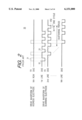
- FIG. 2 illustrates the drive waveform of a DC-type plasma display.
- numeral 30 denotes the drive waveform of the DC type plasma display.
- the electrodes 15 and 16 are driven in a line sequential manner.
- An address pulse 31 having a voltage of VA is supplied depending on a picture signal, to an address electrode 15 which corresponds to the discharge cell in the Nth row.
- a scanning pulse 32 having a voltage of VS is supplied to the scanning electrode 16 in order from the first line.
- the address voltage VA and the scanning voltage VS are simultaneously supplied to a cell. When a voltage between the electrodes 15 and 16 exceeds the discharge starting voltage, the cell is discharged. This discharge is an address discharge.
- the discharge In a fixed period after discharge, the discharge is sustained by a lower voltage than discharge starting voltage because a charged particle is left in the discharged cell. Therefore, in a cell in which an address discharge occurs, the discharge is continued by a sustaining pulse 33 having a voltage of VS2 supplied next to a scanning pulse 32.
- a driving method is called a memory drive method.
- the sub-field system is a method for realizing multiple gradations by dividing one field into plural sub-fields weighted according to the difference in the luminance or brightness and selecting an arbitrary sub-field every pixel according to the amplitude of a signal.
- the word "field” used in this specification means a vertical scanning period and sometimes is called a "frame”, and a "sub-field” is called a "sub-frame”.
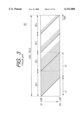
- FIG. 3 illustrates an example of a drive sequence of a prior plasma display apparatus of DC the type.
- a drive sequence 40 utilizing the time sharing drive method shown in FIG. 3 is an example in which an image is displayed in sixteen gradations by four sub-fields SF1 to SF4.
- a scanning period 41 indicates a period for selecting a light emitting cell in a first sub-field and a sustaining period 42 indicates a period in which the selected cell emits light.
- Each sustaining period of the sub-fields SF1 to SF4 is weighted so that the luminance ratio of the sub-fields is 8:4:2:1, and if the luminance of these sub-fields is optionally selected according to the level of an image signal, a display in sixteen gradations equivalent to the fourth power of two is enabled. If the number of gradations is to be increased, the number of sub-fields has only to be increased, and, for example, if the number of sub-fields is eight, and the luminance ratio during the sustaining period is to be selected 128:64:32:16:8:4:2:1, a display in two hundred and fifty-six gradations is enabled. The luminance level of each sub-field is controlled by the number of pulses supplied during the sustaining period.
- This type of plasma display apparatus and the driving method are disclosed, for example, in SID94DIGEST (page 723-726).
- FIG. 4 is a block diagram illustrating the outline of an AC-type plasma display device.
- the plasma display device 20 is constituted by a display panel 21, a plurality of address electrodes 26, a plurality of scanning electrodes 27, a plurality of sustaining electrodes 28, an address pulse generator 22 for driving the address electrodes 26, a scanning and sustaining pulse generator 23 for driving the scanning electrodes 27, a sustaining pulse generator 25 for driving the sustaining electrodes 28, and a signal processing circuit 24 for controlling the generators 22, 23, 25.
- the display panel 21 is provided with two spaced glass plates, the address electrodes 26, the scanning electrodes 27, the sustaining electrodes 28, and a partition for partitioning the space between the glass plates.
- a pixel is constituted by a discharge cell which has space partitioned by the partition between the two glass plates.
- the AC-type plasma display is different from the DC-type display in that an electrode is covered with a dielectric. Rare gas such as He--Xe and Ne--Xe is enclosed in each discharge cell, and if a voltage is applied between the address electrode 26 and the scanning electrode 27, a discharge occurs and ultraviolet rays are generated.
- a color display can be produced by coating every discharge cell with a red, a green and a blue phosphor and by selecting it according to an image signal.
- FIG. 5 illustrates the drive waveform of an AC-type plasma display.
- numeral 50 denotes the drive waveform of the AC-type plasma display.
- the electrodes 26 and 27 are driven in line sequence and an address pulse 51 having a voltage VA is supplied, depending on an image signal, to an address electrode 26 corresponding to a discharge cell in the Nth row.
- a scanning pulse 52 having a voltage VS is supplied in order from the first line to a scanning electrode 27.
- the address voltage VA and the scanning voltage VS are simultaneously supplied to a cell. When the voltage between the address electrode 26 and the scanning electrode 27 exceeds the discharge starting voltage, the cell is discharged.
- this discharge is an address discharge
- a charge is stored on a dielectric covering an electrode (hereinafter called a wall charge), and in a fixed period after it, the discharge can be sustained by a lower voltage than the discharge starting voltage.
- the scanning electrode 27 also functions as a sustaining electrode and a sustaining discharge is caused by alternately supplying a sustaining pulse 53 to the scanning electrode 27 and the sustaining electrode 28.
- the plasma display is referred to an AC type display.
- Such a drive method is called a memory driving method as in the case of the DC type display, and the AC-type plasma display can be driven in a drive sequence 40 as shown in FIG. 3 similar to the DC-type display.
- a memory driving method as in the case of the DC type display
- the AC-type plasma display can be driven in a drive sequence 40 as shown in FIG. 3 similar to the DC-type display.
- another drive sequence is also proposed.
- a drive sequence 60 by a time sharing drive method shown in FIG. 6 is an example of a case in which an image is displayed in sixteen gradations by four sub-fields SF1 to SF4.
- a scanning period 61 is a period for selecting a light emitting cell in a first sub-field SF1
- a sustaining period 62 is a period in which the selected cell emits light.
- Each sustaining period of the sub-fields SF1 to SF4 is weighted so as to have a luminous ratio of 8:4:2:1, and if the luminance of these sub-fields is arbitrarily selected according to the level of an image signal, a display in sixteen gradations equivalent to the fourth power of two is enabled.
- the principle of the time sharing drive method is the same as that of the above DC type shown in FIG. 2, however, the time sharing drive method of the AC type is characterized in that the scanning period 61 and the sustaining period 62 are completely separated and the sustaining pulse 53 common to the whole screen is supplied to the sustaining period 62.
- This type of apparatus is disclosed on pages 7 to 11 in SHINGAKUGIHOU (Communications Institute Technical Report), EID 92-86 issued in January, 1993, for example.
- a disturbance which is referred to as dynamic false contours or quantum noise
- the disturbance or the noise is caused by a change in the light emitting interval which is varied by the display gradations and by the shift of one's eye followed by the dynamic image.
- a high-ranking bit which has large luminous weight, is divided into two and is emitted in different periods.
- the high ranking 4 bit in the sub-fields having a luminous ratio of 8:4:2:1 is assigned to a digital image signal, for example, the highest ranking bit is divided into two and the number of the sub-fields is increased from 4 to 5.
- the luminous ratio of the sub-fields becomes 4:4:2:1:4, and for the highest ranking bit, the first sub-field and the last sub-field are assigned.
- This is one of the ways to decrease or to suppress the dynamic false contours.
- Various proposals for a method for dividing the sub-field and the order for emitting the divided sub-field have been made. This kind of method has been described in, for example, SDI DIGEST 96 (page 291-294).
- a display device which is provided with a high resolution and multiple gradations to correspond to any media.
- a display apparatus for displaying a high resolution image taken by a camera is required.
- plural windows are provided on the screen and a dynamic image is displayed on one of the windows.
- a so-called wide television having an aspect ratio of 16:9 is the subject of increasing interest in the market. Therefore, a dynamic image having an aspect ratio of 16:9 is required for display on a display device having aspect ratio of 3:4.
- the time required for scanning the sub-fields of the XGA display is also 1.6 times that of the VGA display. Therefore, the sustaining period is shortened and sufficient brightness is not obtained, or the number of sub-fields is reduced and sufficient gradations are not obtained. In this case, the image on the XGA display is deteriorated and becomes an unnatural image in comparison with the image of the VGA display.
- An object of the present invention is to provide display apparatus having sufficient gradations or sufficient brightness.
- Another object of the present invention is to provide a display apparatus and a display method for increasing the number of sub-fields.
- a further object of the present invention is to provide a display apparatus and display method for increasing the sustaining period.
- a display apparatus and display method are provided for a display panel having pixels arranged in a matrix form for displaying an image on a effective display area.
- Horizontal electrodes and vertical electrodes are scanned for selectively illuminating said pixels by using a time sharing drive method in which one field period is divided into plural sub-fields weighted according to a sustaining period, wherein an effective display area is divided into plural areas, no scanning for selecting a light emitting pixel is executed in a non-display area, and the number of the above sub-fields is increased in an area in which display in multiple gradations is required in a display area to obtain sufficient gradation.
- the total sustaining period per one field is increased to obtain sufficient brightness.
- another area is provided in which the number of sub-fields is limited to the required minimum in which display in multiple gradations is not required.
- another area having few sub-fields is prepared instead of providing the non-display area.
- FIG. 1 is a block diagram illustrating the outline of a conventional DC-type plasma display device.
- FIG. 2 illustrates an example of the drive waveform of the conventional DC-type plasma display device of FIG. 1.
- FIG. 3 illustrates an example of the drive sequence of the conventional DC-type plasma display device of FIG. 1
- FIG. 4 is a block diagram illustrating the outline of a conventional AC-type plasma display device.
- FIG. 5 illustrates an example of the drive waveform of the conventional AC-type plasma display device of FIG. 4.
- FIG. 6 illustrates an example of the drive sequence of the conventional AC-type plasma display device of FIG. 4.
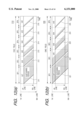
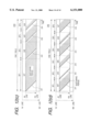
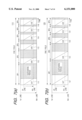
- FIGS. 7(a)-(d) illustrate drive sequences of the present invention.
- FIGS. 8(a)-(c) illustrate an example of the display screen of a display device in a case where the present invention is applied.
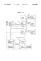
- FIG. 9 is a block diagram illustrating a signal processor according to the present invention.
- FIG. 10 is a block diagram illustrating a scanning pulse generator according to the present invention.
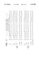
- FIG. 11 is a drive waveform diagram illustrating a scanning pulse of the present invention.
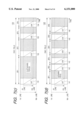
- FIGS. 12(a)-(d) illustrate other drive sequences of the present invention.
- a plasma display device which represents an example of a matrix type display device according to the present invention is constituted by the display panels 11 and 21, the address electrodes 15 and 26, the scanning electrodes 16 and 27, the address pulse generators 12 and 22, the scanning and sustaining pulse generators 13 and 23 and signal processing circuits 14 and 24 for controlling the above generators 12, 22, 13 and 23, as shown in FIGS. 1 and 2.
- the display panel is provided with two spaced glass plates, the address electrodes 15 and 26, the scanning electrodes 16 and 27, and a partition for partitioning the space between the glass plates.
- a pixel has a discharge cell which occupies a space partitioned by the partition between the two glass plates.
- Rare gas such as He--Xe and Ne--Xe is enclosed in each discharge cell, and when a voltage is supplied to the address electrodes 15 and 26 and the scanning electrodes 16 and 27, ultraviolet rays are generated by the gas discharge in the corresponding discharge cell, and the phosphor on the partition is excited and emits light.
- a color display can be produced by coating every discharge cell with a red, a green and a blue phosphor and selecting it according to an image signal.
- FIGS. 7(a) to 7(d) illustrate the embodiments of the present invention in which a drive sequence the same as the sequence 60 shown in FIG. 6 is applied.
- the relationship between the scanning period and the sustaining period is expressed in the following equation:
- Tsus total sustaining period per one field
- Tscn a scanning period per one line
- Li number of scanning line corresponding to No. i sub-field
- FIGS. 7(a) to 7(d) illustrate drive sequences of the present invention.
- FIG. 7(a) illustrates a drive sequence in which only the center part is scanned.
- Numeral 110 designates this drive sequence.
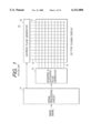
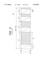
- FIG. 8(a) shows the state of the screen display 610 illustrating a display area and the non-display areas.
- the numeral 611 designates an effective display area in which an image can be displayed.
- the numeral 612 designates a non-display area in which no image is displayed.
- FIG. 8(b) shows the state of the screen display 620 illustrating a display area and a non-display area.
- the numeral 621 denotes an effective display area in which an image can be displayed, which numerals 622 and 623 denote non-display areas in the upper side and in the lower side respectively.
- the scanning period 111 of the drive sequence 110 is shorter than the scanning period 61 of the drive sequence 60. This is because scanning electrodes corresponding to the first line to the Jth line and the Kth line to Nth line in the above non-display areas 612,622 and 623 are not scanned. At the time, the voltage of the electrodes which are not scanned is held at an arbitrary fixed voltage.
- the number of the scanning lines N is 756 lines, which corresponds to the scanning lines of an XGA system
- the number of the scanning lines between the Jth line and Kth line is 480 lines, which corresponds to the scanning lines of the VGA system.
- the number of gradations can be increased to 64 in the drive sequence 110 from 16 in the drive sequence 60.
- FIG. 9 is a block diagram that represents the basic structure of a signal processing circuit to realize the drive sequence according to the present invention, and this circuit is equivalent to the signal processing circuit 14 and the generators 12 and 13 shown in FIG. 1, as well as the signal processing circuit 24 and the generators 22, 23 and 24 shown in FIG. 4.
- An input image signal is written in a frame memory 309 through a digital signal processing circuit 303, after converting the image signal into digital data through an analogue signal processing circuit 301 and an A/D converter 302.
- a control pulse generator 306 various control signals that are necessary for every sub-field are generated.
- the control signal from the control pulse generator 306 is supplied to the digital signal processor 303, and address data is read from the frame memory 309 and is supplied to an address pulse generator 313.
- a system control section 314 there are provided an input signal discriminator 304, a parameter selector 305, a user interface 307, a parameter storage 308 and a data communication interface 310.
- the input signal discriminator 304 the frequency of a synchronizing signal is counted and a signal format is discriminated.
- Information for the signal format is supplied to the parameter selector 305.
- the parameter selector 305 selects a parameter related to a display area which is stored in the parameter storage 308 and the parameter is transmitted to the control pulse generator 306 through a data communication bus 311.
- the control pulse generator 306 controls an address pulse generator 313, a scanning pulse generator 315 and a sustaining pulse generator 316 according to the parameter.
- the parameter related to the display area is selected from the parameter storage 308 as described above, another method for selecting the parameter can be used.
- the parameter selector 305 can be composed of a microcomputer, a parameter related to a scanning area can be calculated from signal format information, outputted from input signal discriminator 304, and supplied to the control pulse generator 306 through the data communication interface 310 and the data communication bus 311 for controlling the parameter of the control pulse generator 306.
- information from information input means 312 is supplied to the parameter selector 305 through the user interface 307 for setting the parameter related to the scanning area.
- the information input means 312 it may take the form of an input device, such as a remote controller, mouse or keyboard.
- a personal computer may be connected to the information input means 312 to transmit image information that is processed using a graphic board in the personal computer to the system control section 314 for setting the scanning area.
- FIG. 10 is a block diagram illustrating the scanning pulse generator 315.
- the scanning pulse generator 315 is composed of several ICs 421, 432, etc. in which several output terminals of each IC are provided. Twelve ICs for the scanning pulse generator are used, if one of the ICs 421 and 432 has 64 output channels and the display has 768 scanning lines corresponding to the XGA system.
- the IC 421 for the scanning pulse generator is composed of a shift resistor 421a, an output control logic circuit 421b, and a high voltage output circuit 421c.
- a data pulse SI from a data input terminal 405 is supplied to the shift-resistor 421a and is converted serial-parallel at the rising edge of a clock signal CK and is supplied to the output control logic 421b.
- the signal from shift-resistor 421a is controlled by the enable signal EN in the output logic circuit 421b and is supplied to the high voltage output circuit 421c, and is outputted from the output 1 to output 64.
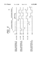
- FIG. 11 illustrates scanning pulses which are generated by the scanning pulse generator shown in FIG. 10.
- the example that the first line to 768th line are scanned and the third line to 766th line are scanned is illustrated.
- the period for generating the scanning pulse is controlled by the enable signal EN in the output control logic circuit 421b.
- the period of the clock signal CK in the scanning pulse generating period and the scanning pulse non-generating period is the same. But any clock duration in the scanning pulse non-generating period may be used.
- the sustaining period can be overlapped with the scanning pulse non-generating period.
- the illustrated scanning pulse generator 315 and the control method of the scanning pulse are one of the embodiments, and any block diagram and scanning pulse control method may be applied for controlling the scanning pulse.
- the control pulse generator 306 changes a scanning pulse control signal by the display area setting parameter which is selected by the parameter selector 305 of the system control section 314, and the generation of the scanning pulse is controlled.
- One of the most important features in the embodiment is that means for discriminating the scanning area or means for setting the scanning area is provided, and the parameter for setting the scanning area is supplied to the control pulse generator 306 for controlling the scanning area.
- the display panel is driven by the method shown in sequence 110.
- the size of the effective display area and the number of display scanning lines may be selected according to the input image signal or user setting.
- FIG. 7(b) illustrates a drive sequence in which a relatively small number of display gradations are applied to some portions of an effective display area and a larger number of display gradations are applied to the center area of the display.
- Numeral 120 denotes the drive sequence shown in FIG. 7(b).
- the state of the display 610 in FIG. 8(a) is that the display area 612 is set to have relatively few display gradations and the display area 611 is set to have a lot of display gradations.
- the display area 621 is set to have a lot of display gradations and the display areas 622 and 623 are set to have relatively few display gradations.
- the scanning periods 121 and 122 of the sequence 120 the first line to the Nth line are scanned, and in the scanning periods 123,124 and 125, the Jth line to the Kth line are scanned. That is, the first line to the Jth line are not scanned in the third, fourth and fifth sub-fields.
- the number of the scanning lines, N is 765 lines which corresponds to the scanning lines of the XGA system
- the number of the scanning lines between the Jth line and the Kth line is 480 lines, which corresponds to the scanning lines of the VGA system.
- the areas 622 and 623 are displayed by two sub-fields and have 4 gradations. From the equation (1), when the number of the sub-fields in the drive sequence 120 is five, the scanning periods between drive sequences 120 and 60 per one field become nearest.
- the number of gradations are increased to 32 from 16 in the drive sequence 60.
- the area that has few display gradations is efficiently used for displaying, for example, an operation menu of the display, or the sub-title information of a film software, etc.
- the voltage between the address electrode 26 and the scanning electrode 27 that correspond to both side areas of the display 611 is determined during scanning periods 123, 124 and 125 such that a discharge does not occur.
- FIG. 7(c) illustrates a drive sequence in which the time gained by shortening the scanning period is assigned to increase the sustaining period for improving the brightness.
- Numeral 130 denotes the drive sequence.
- FIG. 8(a) and FIG. 8(b) show the state of the display screen. In FIG. 8(a), a bright image is displayed in the display area 611 of the display 610, and no image is displayed in the area 612. In FIG. 8(b), a bright image is displayed in the area 621 of the display 620, and no image is displayed in the areas 622 and 623.
- the number of sub-fields of the drive sequence is four
- the number of the scanning lines N is 756 lines, which corresponds to the scanning lines of the XGA system
- the number of the scanning lines between the Jth line and Kth line is 480, which corresponds to the scanning lines of the VGA system.
- the relationship between the scanning period and the sustaining period is expressed by the equation (1). In case the sustaining period is 25 percent of the one field when all lines are scanned, the sustaining period is increased 53 percent by shortening the scanning period. Therefore, the brightness is about double.
- FIG. 7(d) illustrates a drive sequence in which two sub-fields are increased by shortening the scanning period, and one of the sub-fields is used for increasing the display gradations, while the other sub-field is used for reducing the false contour or quantum noise.
- the highest ranking bit which has the largest luminous weight is divided by two and is assigned to the first and sixth sub-fields, so that the illumination time is dispersed. Therefore, the display gradations are increased and the false contour or quantum noise is reduced.
- the embodiments shown in FIGS. 7(a)-(d) are put into practice by using the signal processing circuit shown in FIG. 9 and FIG. 10. By changing the parameter for setting the scanning area in the control pulse generator 306, many display areas may be selected.
- FIG. 7(a)-(d) Various combinations of the embodiments shown in FIG. 7(a)-(d) may be used according to the usage of the display and a variety of signals inputted to the display. In case a display area is further subdivided, the above-mentioned embodiments are basically applied.
- FIG. 8(c) illustrates another embodiment of the display apparatus.
- a display 630 has three display areas 631 632 and 633. An image having few display gradations is displayed in the area 633, and an image having a lot of display gradations is displayed in the area 631, while no image is displayed in the area 632.
- the first area between the first line and the Jth line is not scanned, the second area between the Kth line and the Nth line is scanned a few times and the third area between the Jth line and the Kth line is scanned many times.
- a discharge by a sustaining pulse does not occur in the area to which a scanning pulse is not supplied. Therefore, even if the sustaining pulse is supplied to the scanning electrode 27 and the sustaining electrode 28 which correspond to the non-display area, an image is not displayed. Even if a discharge is not generated, an electric power loss occurs because a pulse is supplied to a capacitive load and a charge and a discharge are repeated.
- plural sustaining pulse generators instead of one generator 314, are provided, and one sustaining pulse generator which corresponds to the non-display area is stopped.
- FIGS. 12(a) to 12(d) illustrate other drive sequences in which the drive sequence 40 is applied to the display in FIGS. 8(a) to 8(c).
- the relationship of the sustaining period to the scanning period in the drive sequence 40 is expressed roughly by the following equation.
- Tsus total sustaining period per one field
- Tscn a scanning period per one line
- Li number of scanning lines corresponding to No. i sub-field
- the scanning period and the sustaining period are fully independent of each other in the driving method shown in FIG. 6, but as for the drive sequence shown in FIG. 3, a scanning period can be overlapped with a previous sustaining period. Therefore, the third member of the equation (2) is added to the equation (1). That is, if an inequality Tv>Tscan ⁇ (L1+L2+. . . Lm) is satisfied, at least a sustaining period corresponding to the third member is obtained.
- the third member of the equation (2) relates to the example where the luminous weight of each sub-field is the second power of 2 like 1:2:4: . . . and if the number of the sub-fields is 8 or less, a sustaining period of 25 percent per one field is acquired.
- FIG. 12(a) illustrates a drive sequence in which the top and bottom area of the display are not scanned and only the center area is scanned.
- Numeral 210 denotes the drive sequence of FIG. 12.
- the state of the screen is such that an image is displayed only on the display area 611 of display 610 of FIG. 8(a) and no image is displayed on the display area 621,
- FIG. 8(b) an image is displayed only on the display area 621 of the display 620 and no image is displayed on the other areas 622 and 623.
- only limited lines from the Jth line to the Kth line are scanned during a scanning period 211216 of the drive sequence shown in FIG.
- the scanning period of the sequence 210 being shorter than that of sequence 60. This is because the lines from the first line to the Jth line and the lines from the Kth line to the Nth line are not scanned in the sequence 210. Supposing that the sustaining period of the drive sequences 40 and 210 is equal to 25 percent of one field period, the number of the scanning lines N is 756 lines, which corresponds to the scanning of the XGA system, and the number of the scanning lines between the Jth line and the Kth line is 480 lines, which corresponds to the scanning of the VGA system.
- the scanning periods between the drive sequences 210 and 40 per one field period become nearest, so that the number of the sub-fields is increased from 4 to 6.
- the luminous weights from the first sub-field to the sixth sub-field are, for example, 32:16:8:4:2:1, and a digitized image data is assigned in order from the highest ranking bit, the number of display gradations is increased to 64 gradations from 16 gradations in the drive sequence 40.
- FIG. 12(b) illustrates a drive sequence in which there are top and bottom areas having few display gradations, and a center area having many display gradations.
- Numeral 220 denotes this drive sequence.
- the state of the screen is such that a display area 611 having a lot of display gradations and a display area 612 having few display gradations are provided as seen in FIG. 8(a). Also, a display area 621 having a lot of display gradations and display areas 622 and 623 having few display gradations are provided as seen in FIG. 8(b).
- Lines from the first line to the Nth line are scanned during scanning periods 221 and 222 of the sequence 220, and lines from the Jth line to the Kth line are scanned during scanning periods 223, 224 and 225 of the sequence 220. This is because lines from the first line to the Nth line and lines from the Kth line to the Nth line are not scanned after the third sub-field.
- the voltage between the address electrode 15 and the scanning electrode 16, which correspond to the areas on both sides of display area 611, are selected so as not to produce a discharge during the scanning periods 223, 224 and 225.
- the sustaining period of the drive sequence 220 is 25 percent of one field period
- the number of the scanning lines N is 756 lines, which corresponds to the scanning lines of the XGA system
- the number of the scanning lines between the Jth line and the Kth line is 480 lines, which corresponds to the scanning lines of the VGA system
- the area having few display gradations is represented by two sub-fields, four gradations. From the equation (2), when the number of sub-fields in the drive sequence 220 is five, the scanning periods between drive sequences 220 and 40 per one field period become nearest, so that number of sub-fields is increased from 4 to 5.
- the number of display gradations is increased to 32 gradations from 16 gradations in the drive sequence 40.
- the area that has few display gradations can be efficiently used by displaying, for example, an operation menu or sub-title information of film software.
- FIG. 12(c) illustrates a drive sequence in which the sustaining period is increased by shortening the scanning period for improving the brightness.
- the state of the screen is such that a bright image is displayed on the display area 611 of the display 610 and no image is displayed on the area 612, as seen in FIG. 8(a). Also, the state of the screen is such that a bright image is displayed on the display area 621 and no image is displayed on the display areas 622 and 623, as seen in FIG. 8(b).
- Numeral 230 denotes the drive sequence of FIG. 12(c).
- the number of sub-fields is 4 in drive sequence 230
- the number of the scanning lines N is 756 lines, which corresponds to the scanning lines of the XGA system
- the number of the scanning lines between the Jth line and the Kth line is 480 lines, which corresponds to the scanning lines of the VGA system.
- the relationship between the scanning period and the sustaining period is expressed by equation (1).
- the maximum sustaining period is about fifty percent of the one field period. Eighty eight percent of one field period is assigned for the sustaining period, and a great deal of improvement in brightness will be achieved, if the shortening of the scanning period is shared with the sustaining period.
- FIG. 12(d) illustrates a drive sequence in which two sub-fields are increased by shortening the scanning period, and one of the sub-fields is used for increasing the display gradations, while the other sub-field is used for reducing the false contour or quantum noise which occurs in case of displaying motion or a dynamic image.
- the highest ranking bit which has the largest luminous weight is divided by two and is assigned to the first and the sixth sub-fields, so that the luminous time is dispersed. Therefore, the display gradations are increased and the false contour or quantum noise is reduced.
- the effect of the embodiments shown in FIGS. 12(a)-(d) is the same as that provided by the embodiments shown in FIGS. 7(a)-(b).
- FIGS. 12(a)-(d) are put into practice by using the signal processing circuit shown in FIG. 9 and FIG. 10. By changing the parameter for setting the scanning area in the control pulse generator 306, various display areas may be obtained. Many combination of the embodiments shown in FIGS. 12(a)-(d) may be used according to the usage of the display and a variety of signals inputted to the display.
- the number of sub-fields is set to four to facilitate the description, however, the number is not limited to four and may be set to an arbitrary number.
- An image in each sub-field may be displayed in an arbitrary order.
- the luminous weight of a sub-field may be changed. If the number of sub-fields is changed depending upon a display area, the number and order of sub-fields allocated to the respective areas also may be arbitrarily selected.
- a high resolution screen such as SVGA (800 ⁇ 600 dots), XGA (1024 ⁇ 768 dots) and SXGA (1280 ⁇ 1024 dots)
- SVGA 800 ⁇ 600 dots
- XGA XGA (1024 ⁇ 768 dots)
- SXGA 1280 ⁇ 1024 dots
Landscapes
- Engineering & Computer Science (AREA)
- Physics & Mathematics (AREA)
- Computer Hardware Design (AREA)
- General Physics & Mathematics (AREA)
- Theoretical Computer Science (AREA)
- Power Engineering (AREA)
- Plasma & Fusion (AREA)
- Control Of Indicators Other Than Cathode Ray Tubes (AREA)
- Control Of Gas Discharge Display Tubes (AREA)
Applications Claiming Priority (2)
| Application Number | Priority Date | Filing Date | Title |
|---|---|---|---|
| JP11769196 | 1996-05-13 | ||
| JP8-117691 | 1996-05-13 |
Publications (1)
| Publication Number | Publication Date |
|---|---|
| US6151000A true US6151000A (en) | 2000-11-21 |
Family
ID=14717918
Family Applications (1)
| Application Number | Title | Priority Date | Filing Date |
|---|---|---|---|
| US08/854,640 Expired - Fee Related US6151000A (en) | 1996-05-13 | 1997-05-12 | Display apparatus and display method thereof |
Country Status (3)
| Country | Link |
|---|---|
| US (1) | US6151000A (fr) |
| EP (1) | EP0807919A1 (fr) |
| KR (1) | KR970076451A (fr) |
Cited By (15)
| Publication number | Priority date | Publication date | Assignee | Title |
|---|---|---|---|---|
| US6373477B1 (en) * | 1998-03-23 | 2002-04-16 | U.S. Philips Corporation | Display driving |
| US6414657B1 (en) | 1997-12-10 | 2002-07-02 | Matsushita Electric Industrial Co., Ltd. | Detector for detecting pseudo-contour noise and display apparatus using the detector |
| US6433763B1 (en) * | 1998-06-27 | 2002-08-13 | Lg Electronics, Inc. | Plasma display panel drive method and apparatus |
| US6559814B1 (en) * | 1998-10-01 | 2003-05-06 | Fujitsu Limited | Driving plasma display panel without visible flickering |
| US6563486B2 (en) * | 1995-10-24 | 2003-05-13 | Fujitsu Limited | Display driving method and apparatus |
| WO2003063118A3 (fr) * | 2002-01-23 | 2003-12-31 | Koninkl Philips Electronics Nv | Adressage de cellules d'ecran |
| US20040125050A1 (en) * | 2002-12-27 | 2004-07-01 | Fujitsu Hitachi Plasma Display Limited | Method for driving plasma display panel, and plasma display device |
| US20040130560A1 (en) * | 2002-11-01 | 2004-07-08 | Seiko Epson Corporation | Electro-optical device, method of driving electro-optical device, and electronic apparatus |
| US20050093778A1 (en) * | 2003-10-30 | 2005-05-05 | Joon-Koo Kim | Panel driving method and apparatus |
| US7002605B1 (en) * | 2000-07-03 | 2006-02-21 | Alps Electric Co., Ltd. | Image display apparatus for fixing luminance of blank area and varying only luminance of image |
| US20060262040A1 (en) * | 2005-05-23 | 2006-11-23 | Lg Electronics Inc. | Plasma display driving apparatus and driving method |
| EP2276016A1 (fr) * | 2009-07-17 | 2011-01-19 | Samsung Electronics Co., Ltd. | Appareil et procédé d'affichage |
| TWI548953B (zh) * | 2008-05-13 | 2016-09-11 | 尼康股份有限公司 | A moving body system and a moving body driving method, a pattern forming apparatus and a pattern forming method, an exposure apparatus and an exposure method, and an element manufacturing method |
| US10347173B2 (en) * | 2014-12-24 | 2019-07-09 | Lg Display Co., Ltd. | Organic light emitting diode display and method for driving the same |
| CN112017602A (zh) * | 2020-09-02 | 2020-12-01 | Tcl华星光电技术有限公司 | mini LED背光模组的驱动方法 |
Families Citing this family (2)
| Publication number | Priority date | Publication date | Assignee | Title |
|---|---|---|---|---|
| DE19856436A1 (de) | 1998-12-08 | 2000-06-15 | Thomson Brandt Gmbh | Verfahren zum Ansteuern eines Plasmabildschirms |
| WO2004051611A1 (fr) * | 2002-11-29 | 2004-06-17 | Koninklijke Philips Electronics N.V. | Sous-champ d'entrainement de pixels dans un dispositif d'affichage |
Citations (11)
| Publication number | Priority date | Publication date | Assignee | Title |
|---|---|---|---|---|
| EP0295691A2 (fr) * | 1987-06-19 | 1988-12-21 | Kabushiki Kaisha Toshiba | Système de commutation du mode d'affichage pour un appareil de visualisation à plasma |
| EP0295690A2 (fr) * | 1987-06-19 | 1988-12-21 | Kabushiki Kaisha Toshiba | Système de commande de la zone de visualisation pour un dispositif d'affichage à plasma |
| US4891705A (en) * | 1987-11-30 | 1990-01-02 | Nec Corporation | Apparatus for generating a picture signal at precise horizontal position |
| US4965563A (en) * | 1987-09-30 | 1990-10-23 | Hitachi, Ltd. | Flat display driving circuit for a display containing margins |
| US5111190A (en) * | 1988-05-28 | 1992-05-05 | Kabushiki Kaisha Toshiba | Plasma display control system |
| EP0488326A2 (fr) * | 1990-11-28 | 1992-06-03 | Nec Corporation | Méthode de commande pour un panneau d'affichage à plasma |
| WO1994009473A1 (fr) * | 1992-10-15 | 1994-04-28 | Rank Brimar Limited | Dispositif de visualisation |
| US5396258A (en) * | 1988-05-28 | 1995-03-07 | Kabushiki Kaisha Toshiba | Plasma display control system |
| US5448260A (en) * | 1990-05-07 | 1995-09-05 | Kabushiki Kaisha Toshiba | Color LCD display control system |
| US5844534A (en) * | 1993-12-28 | 1998-12-01 | Kabushiki Kaisha Toshiba | Liquid crystal display apparatus |
| US5856823A (en) * | 1994-10-28 | 1999-01-05 | Matsushita Electric Industrial Co., Ltd. | Plasma display |
-
1997
- 1997-05-09 KR KR1019970017863A patent/KR970076451A/ko not_active Ceased
- 1997-05-09 EP EP97107631A patent/EP0807919A1/fr not_active Withdrawn
- 1997-05-12 US US08/854,640 patent/US6151000A/en not_active Expired - Fee Related
Patent Citations (14)
| Publication number | Priority date | Publication date | Assignee | Title |
|---|---|---|---|---|
| EP0295691A2 (fr) * | 1987-06-19 | 1988-12-21 | Kabushiki Kaisha Toshiba | Système de commutation du mode d'affichage pour un appareil de visualisation à plasma |
| EP0295690A2 (fr) * | 1987-06-19 | 1988-12-21 | Kabushiki Kaisha Toshiba | Système de commande de la zone de visualisation pour un dispositif d'affichage à plasma |
| US4990904A (en) * | 1987-06-19 | 1991-02-05 | Kabushiki Kaisha Toshiba | Display mode switching system for flat panel display apparatus |
| US4965563A (en) * | 1987-09-30 | 1990-10-23 | Hitachi, Ltd. | Flat display driving circuit for a display containing margins |
| US4891705A (en) * | 1987-11-30 | 1990-01-02 | Nec Corporation | Apparatus for generating a picture signal at precise horizontal position |
| US5396258A (en) * | 1988-05-28 | 1995-03-07 | Kabushiki Kaisha Toshiba | Plasma display control system |
| US5111190A (en) * | 1988-05-28 | 1992-05-05 | Kabushiki Kaisha Toshiba | Plasma display control system |
| US5592187A (en) * | 1988-05-28 | 1997-01-07 | Kabushiki Kaisha Toshiba | Plasma display control system |
| US5448260A (en) * | 1990-05-07 | 1995-09-05 | Kabushiki Kaisha Toshiba | Color LCD display control system |
| EP0488326A2 (fr) * | 1990-11-28 | 1992-06-03 | Nec Corporation | Méthode de commande pour un panneau d'affichage à plasma |
| US5317334A (en) * | 1990-11-28 | 1994-05-31 | Nec Corporation | Method for driving a plasma dislay panel |
| WO1994009473A1 (fr) * | 1992-10-15 | 1994-04-28 | Rank Brimar Limited | Dispositif de visualisation |
| US5844534A (en) * | 1993-12-28 | 1998-12-01 | Kabushiki Kaisha Toshiba | Liquid crystal display apparatus |
| US5856823A (en) * | 1994-10-28 | 1999-01-05 | Matsushita Electric Industrial Co., Ltd. | Plasma display |
Non-Patent Citations (6)
| Title |
|---|
| Communications Institute Technical Report, EID 92 86 issued in Jan., 1993. * |
| Communications Institute Technical Report, EID 92-86 issued in Jan., 1993. |
| SID94DIGEST ( pp. 723 726). by T. Tamura, et al. * |
| SID94DIGEST ( pp. 723-726). by T. Tamura, et al. |
| SID96DIGEST(pp. 291 294). by T. Yamaguchi, et al. * |
| SID96DIGEST(pp. 291-294). by T. Yamaguchi, et al. |
Cited By (21)
| Publication number | Priority date | Publication date | Assignee | Title |
|---|---|---|---|---|
| US6563486B2 (en) * | 1995-10-24 | 2003-05-13 | Fujitsu Limited | Display driving method and apparatus |
| US7855698B2 (en) | 1995-10-24 | 2010-12-21 | Hitachi Limited | Display driving method and apparatus |
| US20060279482A1 (en) * | 1995-10-24 | 2006-12-14 | Hitachi, Ltd | Display driving method and apparatus |
| US6414657B1 (en) | 1997-12-10 | 2002-07-02 | Matsushita Electric Industrial Co., Ltd. | Detector for detecting pseudo-contour noise and display apparatus using the detector |
| US6812932B2 (en) | 1997-12-10 | 2004-11-02 | Matsushita Electric Industrial Co., Ltd. | Detector for detecting pseudo-contour noise and display apparatus using the detector |
| US6373477B1 (en) * | 1998-03-23 | 2002-04-16 | U.S. Philips Corporation | Display driving |
| US6433763B1 (en) * | 1998-06-27 | 2002-08-13 | Lg Electronics, Inc. | Plasma display panel drive method and apparatus |
| US6559814B1 (en) * | 1998-10-01 | 2003-05-06 | Fujitsu Limited | Driving plasma display panel without visible flickering |
| US7002605B1 (en) * | 2000-07-03 | 2006-02-21 | Alps Electric Co., Ltd. | Image display apparatus for fixing luminance of blank area and varying only luminance of image |
| WO2003063118A3 (fr) * | 2002-01-23 | 2003-12-31 | Koninkl Philips Electronics Nv | Adressage de cellules d'ecran |
| US20040130560A1 (en) * | 2002-11-01 | 2004-07-08 | Seiko Epson Corporation | Electro-optical device, method of driving electro-optical device, and electronic apparatus |
| US20040125050A1 (en) * | 2002-12-27 | 2004-07-01 | Fujitsu Hitachi Plasma Display Limited | Method for driving plasma display panel, and plasma display device |
| US20050093778A1 (en) * | 2003-10-30 | 2005-05-05 | Joon-Koo Kim | Panel driving method and apparatus |
| US20060262040A1 (en) * | 2005-05-23 | 2006-11-23 | Lg Electronics Inc. | Plasma display driving apparatus and driving method |
| TWI548953B (zh) * | 2008-05-13 | 2016-09-11 | 尼康股份有限公司 | A moving body system and a moving body driving method, a pattern forming apparatus and a pattern forming method, an exposure apparatus and an exposure method, and an element manufacturing method |
| EP2276016A1 (fr) * | 2009-07-17 | 2011-01-19 | Samsung Electronics Co., Ltd. | Appareil et procédé d'affichage |
| US20110012890A1 (en) * | 2009-07-17 | 2011-01-20 | Samsung Electronics Co., Ltd. | Display apparatus and display method |
| US10347173B2 (en) * | 2014-12-24 | 2019-07-09 | Lg Display Co., Ltd. | Organic light emitting diode display and method for driving the same |
| CN112017602A (zh) * | 2020-09-02 | 2020-12-01 | Tcl华星光电技术有限公司 | mini LED背光模组的驱动方法 |
| WO2022047922A1 (fr) * | 2020-09-02 | 2022-03-10 | Tcl华星光电技术有限公司 | Procédé de commande pour module de rétroéclairage à mini-del |
| US11694642B2 (en) | 2020-09-02 | 2023-07-04 | Tcl China Star Optoelectronics Technology Co., Ltd. | Method for driving mini-LED backlight module |
Also Published As
| Publication number | Publication date |
|---|---|
| KR970076451A (ko) | 1997-12-12 |
| EP0807919A1 (fr) | 1997-11-19 |
Similar Documents
| Publication | Publication Date | Title |
|---|---|---|
| US6151000A (en) | Display apparatus and display method thereof | |
| US6097358A (en) | AC plasma display with precise relationships in regards to order and value of the weighted luminance of sub-fields with in the sub-groups and erase addressing in all address periods | |
| KR100306987B1 (ko) | 계조표시방법및계조표시장치 | |
| JP2903984B2 (ja) | ディスプレイ装置の駆動方法 | |
| US6297788B1 (en) | Half tone display method of display panel | |
| US5818419A (en) | Display device and method for driving the same | |
| US5436634A (en) | Plasma display panel device and method of driving the same | |
| EP1085495B1 (fr) | Panneau d'affichage à plasma | |
| KR100454786B1 (ko) | 텔레비젼화상신호의계조표시방법및그장치 | |
| US6710755B1 (en) | Method for driving plasma display panel | |
| US6924778B2 (en) | Method and device for implementing subframe display to reduce the pseudo contour in plasma display panels | |
| US7460139B2 (en) | Method and apparatus of driving a plasma display panel | |
| CN100504984C (zh) | 用于显示等离子体显示面板灰度的方法和装置 | |
| JP3430593B2 (ja) | ディスプレイ装置の駆動方法 | |
| US20030137473A1 (en) | Method and apparatus for processing video pictures | |
| JP2001242826A (ja) | プラズマディスプレイ装置及びその駆動方法 | |
| US7053870B2 (en) | Drive method for plasma display panel and plasma display device | |
| US20020140636A1 (en) | Matrix display device and method | |
| US6052101A (en) | Circuit of driving plasma display device and gray scale implementing method | |
| US7123217B2 (en) | Method for driving plasma display panel | |
| JP2000035774A (ja) | 表示装置 | |
| JPH1055151A (ja) | ディスプレイ装置 | |
| US20010013845A1 (en) | Mehtod of driving a plasma display panel before erase addressing | |
| JP2000172225A (ja) | 表示装置 | |
| US7109950B2 (en) | Display apparatus |
Legal Events
| Date | Code | Title | Description |
|---|---|---|---|
| AS | Assignment |
Owner name: HITACHI LTD., JAPAN Free format text: ASSIGNMENT OF ASSIGNORS INTEREST;ASSIGNORS:OHTAKA, HIROSHI;ISHIGAKI, MASAJI;NOGUCHI, YASUJI;AND OTHERS;REEL/FRAME:008556/0916 Effective date: 19970421 |
|
| FEPP | Fee payment procedure |
Free format text: PAYOR NUMBER ASSIGNED (ORIGINAL EVENT CODE: ASPN); ENTITY STATUS OF PATENT OWNER: LARGE ENTITY |
|
| FPAY | Fee payment |
Year of fee payment: 4 |
|
| REMI | Maintenance fee reminder mailed | ||
| LAPS | Lapse for failure to pay maintenance fees | ||
| STCH | Information on status: patent discontinuation |
Free format text: PATENT EXPIRED DUE TO NONPAYMENT OF MAINTENANCE FEES UNDER 37 CFR 1.362 |
|
| FP | Lapsed due to failure to pay maintenance fee |
Effective date: 20081121 |