US6262425B1 - Curvilinear axis set-up for charged particle lithography - Google Patents
Curvilinear axis set-up for charged particle lithography Download PDFInfo
- Publication number
- US6262425B1 US6262425B1 US09/266,335 US26633599A US6262425B1 US 6262425 B1 US6262425 B1 US 6262425B1 US 26633599 A US26633599 A US 26633599A US 6262425 B1 US6262425 B1 US 6262425B1
- Authority
- US
- United States
- Prior art keywords
- charged particle
- particle beam
- deflection
- deflectors
- recited
- Prior art date
- Legal status (The legal status is an assumption and is not a legal conclusion. Google has not performed a legal analysis and makes no representation as to the accuracy of the status listed.)
- Expired - Lifetime
Links
- 239000002245 particle Substances 0.000 title claims abstract description 44
- 238000001459 lithography Methods 0.000 title description 5
- 238000012937 correction Methods 0.000 claims abstract description 13
- 230000003068 static effect Effects 0.000 claims abstract description 7
- 238000000034 method Methods 0.000 claims description 45
- 238000010894 electron beam technology Methods 0.000 claims description 10
- 230000000694 effects Effects 0.000 description 10
- 230000003287 optical effect Effects 0.000 description 9
- 230000035945 sensitivity Effects 0.000 description 8
- 230000005670 electromagnetic radiation Effects 0.000 description 5
- 230000006870 function Effects 0.000 description 5
- 238000004519 manufacturing process Methods 0.000 description 5
- 230000008569 process Effects 0.000 description 5
- 230000004075 alteration Effects 0.000 description 4
- 230000003993 interaction Effects 0.000 description 4
- 238000006073 displacement reaction Methods 0.000 description 3
- 150000002500 ions Chemical class 0.000 description 3
- 238000004804 winding Methods 0.000 description 3
- 230000009471 action Effects 0.000 description 2
- 238000005516 engineering process Methods 0.000 description 2
- 230000005855 radiation Effects 0.000 description 2
- 230000004044 response Effects 0.000 description 2
- 230000009466 transformation Effects 0.000 description 2
- 230000008901 benefit Effects 0.000 description 1
- 230000015556 catabolic process Effects 0.000 description 1
- 230000008859 change Effects 0.000 description 1
- AFYCEAFSNDLKSX-UHFFFAOYSA-N coumarin 460 Chemical compound CC1=CC(=O)OC2=CC(N(CC)CC)=CC=C21 AFYCEAFSNDLKSX-UHFFFAOYSA-N 0.000 description 1
- 238000006880 cross-coupling reaction Methods 0.000 description 1
- 230000001186 cumulative effect Effects 0.000 description 1
- 238000006731 degradation reaction Methods 0.000 description 1
- 230000001419 dependent effect Effects 0.000 description 1
- 238000009826 distribution Methods 0.000 description 1
- 230000005684 electric field Effects 0.000 description 1
- 230000005284 excitation Effects 0.000 description 1
- 238000002474 experimental method Methods 0.000 description 1
- 230000033001 locomotion Effects 0.000 description 1
- 239000000463 material Substances 0.000 description 1
- 230000004048 modification Effects 0.000 description 1
- 238000012986 modification Methods 0.000 description 1
- 230000009467 reduction Effects 0.000 description 1
- 238000011160 research Methods 0.000 description 1
- 239000004065 semiconductor Substances 0.000 description 1
- 239000007787 solid Substances 0.000 description 1
Images






Classifications
-
- B—PERFORMING OPERATIONS; TRANSPORTING
- B82—NANOTECHNOLOGY
- B82Y—SPECIFIC USES OR APPLICATIONS OF NANOSTRUCTURES; MEASUREMENT OR ANALYSIS OF NANOSTRUCTURES; MANUFACTURE OR TREATMENT OF NANOSTRUCTURES
- B82Y10/00—Nanotechnology for information processing, storage or transmission, e.g. quantum computing or single electron logic
-
- H—ELECTRICITY
- H01—ELECTRIC ELEMENTS
- H01J—ELECTRIC DISCHARGE TUBES OR DISCHARGE LAMPS
- H01J37/00—Discharge tubes with provision for introducing objects or material to be exposed to the discharge, e.g. for the purpose of examination or processing thereof
- H01J37/30—Electron-beam or ion-beam tubes for localised treatment of objects
- H01J37/317—Electron-beam or ion-beam tubes for localised treatment of objects for changing properties of the objects or for applying thin layers thereon, e.g. for ion implantation
- H01J37/3174—Particle-beam lithography, e.g. electron beam lithography
-
- B—PERFORMING OPERATIONS; TRANSPORTING
- B82—NANOTECHNOLOGY
- B82Y—SPECIFIC USES OR APPLICATIONS OF NANOSTRUCTURES; MEASUREMENT OR ANALYSIS OF NANOSTRUCTURES; MANUFACTURE OR TREATMENT OF NANOSTRUCTURES
- B82Y40/00—Manufacture or treatment of nanostructures
-
- H—ELECTRICITY
- H01—ELECTRIC ELEMENTS
- H01J—ELECTRIC DISCHARGE TUBES OR DISCHARGE LAMPS
- H01J37/00—Discharge tubes with provision for introducing objects or material to be exposed to the discharge, e.g. for the purpose of examination or processing thereof
- H01J37/02—Details
- H01J37/04—Arrangements of electrodes and associated parts for generating or controlling the discharge, e.g. electron-optical arrangement or ion-optical arrangement
- H01J37/147—Arrangements for directing or deflecting the discharge along a desired path
- H01J37/1472—Deflecting along given lines
Definitions
- the present invention generally relates to high resolution lithography systems using charged particles for exposure of a resist and, more particularly, to alignment procedures for forcing a charged particle beam to follow a planar curvilinear trajectory.
- Lithographic processes are generally required in the manufacture of semiconductor integrated circuits. Even though there is a trend in the manufacture of integrated circuits to employ processes and element designs in which many processes are carried out in a self-aligned manner (both to avoid some lithographic processes and to produce structures at smaller size than can be accomplished lithographically), at least one lithographic process to define element locations is invariably required.
- the small feature sizes of modern and foreseeable integrated circuits require extremely high-resolution exposures of the resist to be made.
- the lithographic technology almost exclusively in use in the industry at the present time is based on the use of electromagnetic radiation (EMR) as the exposure medium of choice to expose the resist.
- EMR electromagnetic radiation
- Optical technology has advanced to the point that resolution is essentially limited by diffraction (or, more generally, interference effects of the radiation) but not significantly by imperfections of the optics known as aberrations. Diffraction is determined by the wavelength of the light used to expose the resist and is of generally lesser impact at shorter wavelengths.
- a magnetic field will alter the trajectory of the individual electrons in the beam.
- the distribution of motions of the individual electrons will generally be such that the electrons can be collectively treated as a beam even though the beam may be relatively diffuse over much of its length, as alluded to above.
- the electron or electron beam trajectory, off the electron-optical axis of a lens will generally have a characteristically helical component imparted by magnetic lens fields in the electron-optical system.
- a special case of the electron beam trajectory occurs, however, if a component of the radial field of a lens is canceled by a suitably aligned deflection field, hereafter referred to as an axis-compensation field.
- the curvilinear axis of the beam will theoretically be confined to a plane which also contains the axis of the e-beam system.
- correct alignment of the axis-compensation fields, to confine the beam to a planar path along the column length is very difficult to achieve.
- the general case of the curvilinear deflection is one which does not restrict the beam to lie within a plane.
- resolution is sensitive to beam position.
- resolution will be optimized.
- Such a beam path can be predicted by currently available, computer-implemented modeling techniques which can then specify excitation values for the various deflectors and lenses of the system.
- modeling techniques which assume ideal or at least well-behaved lens and deflector performance do not provide sufficiently accurate information to maximize resolution. Accordingly, an experimental technique is necessary to assure that the electron beam follows the correct optical path in practice.
- Misalignment of the axis-compensation field with the radial field component of a lens also leads to subfield distortions and placement errors. Such errors can occur by misalignment at any electron-optical element (which will generally number between ten and twenty) of the e-beam tool and the distortion and placement errors are potentially cumulative throughout the e-beam column of the tool.
- alignment is determined by reference to variable-width slit apertures located within the vacuum of a charged-particle column.
- the beam is statically deflected in one direction to it's maximum extent, using all of the deflectors above the aperture plate of interest, then it is scanned in two orthogonal directions by one or more deflectors above the aperture plate of interest over the edges of a given aperture plate and the beam current is recorded as it is intercepted on the aperture plate.
- the beam is then statically deflected in the opposite direction to it's maximum extent, and then is scanned in two orthogonal directions by one or more deflectors above the aperture plate of interest over the edges of the same aperture plate and the beam current recorded as it is intercepted on the aperture. From the intercepted current on the aperture, as a function of the two sets of scans, the beam position is established, and means are provided for correcting the trajectory so that it matches that which is predicted by theory. Iterations of this procedure over the length of the column establish a desired curvilinear path.
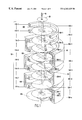
- FIG. 1 is a schematic representation of a section of a projection lithography tool, illustrating magnetic lenses, deflecting and axis-compensation yokes, as well as variable-width slit apertures on which the invention is implemented;
- FIG. 2 is a schematic representation of an individual variable-width slit aperture
- FIG. 3 is a schematic representation of a series of variable-width slit apertures
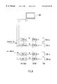
- FIG. 4 is a schematic representation of the deflection electronics and control system
- FIG. 5 is a schematic representation of a deflected beam in relation to a variable-width slit aperture, with the deflection gain and axis-compensation terms adjusted correctly,
- FIG. 6 is a schematic representation of a deflected beam in relation to a variable-width slit aperture, with the deflection gain and axis-compensation terms misadjusted,
- FIG. 7 is a two-dimensional image of the intercepted current onto a variable-width slit aperture from a “reduction to practice” setup of the invention
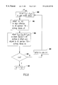
- FIG. 8 is a flowchart discussing details of the Curvilinear axis setup technique, performed with magnetic lenses off in the vicinity of the magnetic yokes and
- FIG. 9 is a flowchart discussing additional details of the Curvilinear axis setup technique, performed with the magnetic yokes energized.
- FIG. 10 is a pictoral representation of the 4 steps described herein for setting up the deflection to follow the Curvilinear axis.
- FIG. 1 there is shown a section of a projection system 50 of the type described in U.S. Pat. No. 5,635,719.
- Lens coils such as 90 , 101 and 102 are shown symbolically as single coils, but may consist of a plurality of coils or windings to generate a magnetic field of the appropriate shape used to project an image of a beam-defining aperture contained in the upper-column optics shown symbolically as 20 to a reticle subfield 103 and finally to the target 104 .
- lens 101 collimates the image of the reticle subfield, 103 , whereas lens 102 projects the image to the target 104 . Additionally, lens coil 101 images the charged-particle beam crossover to the back focal point 105 of the projector lens 102 .
- Highly-stable current drivers provide the static current, and adjustment for these and other lenses in the charged-particle system.
- deflectors 110 - 1 to 110 -n Shown distributed preferably uniformly along the axial direction, throughout the illuminator 90 , collimator 101 and projector 102 are deflectors 110 - 1 to 110 -n, axis compensation yokes 120 - 1 to 120 -n, and variable-width slit apertures 150 - 1 to 150 -n.
- the vertical dots in FIG. 1, between the deflectors 110 - 1 to 110 -n and the axis compensation yokes 120 - 1 to 120 -n indicate that either fewer or additional deflectors and/or axis compensation yokes could be included in the projection system as desired, but for ease of viewing, only 7 are shown.
- the deflectors above the reticle 103 are analogous to those shown in FIG. 1 in U.S. Pat. No. 5,635,719 as 5 , 7 , 55 and 57 .
- the deflectors between the reticle 103 and target 104 are analogous to those shown in FIG. 1 in U.S. Pat. No. 5,635,719 as 105 , 107 , 205 and 207 therein and the axis-compensation yokes are analogous to those in the aforementioned patent, FIG. 1, 150 - 1 to 150 -n and 250 - 1 to 250 -n.
- axis-compensation yokes are included above the reticle 103 , as shown in FIG. 1 .
- each deflector, 110 - 1 to 110 -n has associated with it, an axis compensation yoke 120 - 1 to 120 -n, at the same axial position.
- the deflection field can be oriented to occur in one axis and the axis compensation field in an orthogonal axis, and thus a single yoke consisting of windings that generate magnetic fields in mutually orthogonal orientations can be used as both deflection and axis compensation yokes.
- electric deflectors could be used in place of the magnetic deflectors.
- the subfields at the reticle are on the order of 1 mm 2
- the magnification of the projection system is on the order of 1 ⁇ 4 or, alternatively expressed, a demagnification ratio of 4:1.
- the shape and dimensions of the beam as it propagates from the reticle to the target therefore varies from square (at the reticle 103 and target 104 ) to Gaussian (at the back focal point, 105 , of the projector lens 102 ) and from ⁇ 1 mm to ⁇ 1 ⁇ 4 mm from the reticle to the target.
- each deflection yoke 110 - 1 to 110 -n (and axis-compensation yokes 120 - 1 to 120 -n) is a variable-width slit aperture, 150 - 1 to 150 -n.
- the preferred geometry of one such variable-width slit aperture is shown in FIG. 2 . It is recognized that other shapes for the opening are possible, but for clarity, one such shape is shown herein to convey an understanding of the principles of the invention.
- the opening, 165 in the aperture plate 160 is keyhole-shaped and rectangular.
- the narrower dimension 170 of the opening 165 is several times greater than the maximum extent of the beam.
- each variable-width slit aperture 150 - 1 to 150 -n is deflected using all of the deflectors above each variable-width slit aperture 150 - 1 to 150 -n, then scanned using one or two deflection yokes immediately above the variable-width aperture of interest.
- the width 180 of each variable-width aperture in the example shown in FIG. 2 is thus made slightly larger than the expected position of the beam when deflected at the axial position of each of the variable-width slit apertures 150 - 1 to 150 -n.
- Curve 165 in FIG. 3 of U.S. Pat. No. 5,635,719 shows an example of the radial position of a beam of particles as it travels from the reticle to the target.
- the overall path of the beam is shown in FIG. 3 of the present application.
- Many variable-width slit apertures are shown in this figure, both above and below the plane of the reticle 103 .
- the number of yokes and variable-width slit apertures is chosen so that the planar deflection (and axis-compensation) is smoothly-varying, axially.
- the length 170 of the opening 165 in the aperture plate 160 is 3 mm, and the width 180 is 3 mm longer than the expected deflection at axial location of the apertures 150 - 1 to 150 -n, as calculated. Errors in the position of the undeflected beam are thus detectable by current intercepted by the aperture plate at corners of the “keyhole” shape formed by the longer portion 190 of the variable width slit aperture.
- 2 located in the center of the aperture plate 160 is 2 mm long (beyond the 3 mm length of the opening as described above) and 2 mm wide, and is used to assess the alignment of the beam in the undeflected condition, relative to the position of the slit aperture, as discussed below.
- the long-axis, 180 of each of the variable-width slit apertures 150 - 1 to 150 -n have been oriented, rotationally, such that they are aligned to the desired planar deflection direction. It is further assumed, that this direction lies along one of the orthogonal axes of both the reticle and the wafer stages, that is the long axis of the variable-width slit apertures lie along either the “X” or the “Y” stage axes.
- the apertures could be rotated away from the “X” and “Y” stage directions. In this case, the rotational angle of each aperture could be adjusted to match the predictions from a model.
- variable curvilinear axis describes a planar deflection above and below a reticle.
- deflection yokes 110 - 1 to 110 -n and axis-compensation yokes 120 - 1 to 120 -n the deflection trajectory would be helical.
- the object of this invention is to describe a technique for determining the current applied to both the deflection 110 - 1 to 110 -n and axis-compensation yokes 120 - 1 to 120 -n, such that the deflection of the beam is planar, and that the beam has the proper radial displacement at the position of each of the variable-width slit apertures in the electron beam column.
- FIG. 4 shows schematically a control computer, and other elements which allow for a manual or automatic setup of the currents required for the deflection and axis-shifting yokes so that the beam's deflection is planar and lies along the predetermined planar curvilinear path.
- the functions of the deflection and axis-shifting yokes could be performed, by electrostatic deflection elements.
- the terms “current” and “current drivers” could be replaced with “voltage” and “voltage drivers” if the deflection and axis-shifting yokes were electrostatic rather then magnetic.
- each deflection yoke 110 - 1 to 110 -n and axis-compensation yoke 120 - 1 to 120 -n are described as being physically part of the same yoke, i.e., deflection yoke 110 - 1 , and axis-compensating yoke 120 - 1 , are orthogonal axes of the same yoke, and so on.
- yokes 200 - 1 to 200 -n the combination of deflection yokes 110 - 1 to 110 -n and axis-compensation yokes 120 - 1 to 120 -n, will be referred to as yokes 200 - 1 to 200 -n.
- Each such yoke ( 200 - 1 , 200 -n) is oriented, rotationally, such that the deflection of the beam (caused by deflection yoke 110 - 1 ), in the absence of a lens field, lies generally along the long axis 180 of the variable-width slit apertures, 150 - 1 to 150 -n (Y axis) and the axis-shifting yoke ( 120 - 1 to 120 -n), deflects the beam in the orthogonal direction with respect to the deflection yoke ( 110 - 1 ), or along the narrow direction 170 of the variable-width slit apertures 150 - 1 to 150 -n (X axis).
- magnetic current drivers 210 - 1 to 210 -n are connected to each of the deflection yokes 110 - 1 to 110 -n.
- magnetic current drivers 220 - 1 to 220 -n are connected to each of the axis-compensation yokes 120 - 1 to 120 -n.
- the magnetic predrivers, 310 - 1 to 310 -n and 320 - 1 to 320 -n contain multiplying Digital to Analog Converters (MDAC's).
- MDAC Digital to Analog Converter
- the software in the control computer, 300 performs mathematical transforms to control the outputs of the magnetic predrivers 310 - 1 to 310 -n and 320 - 1 to 320 -n.
- variables Y i and X i refer to the voltage output of the i th deflection ( 310 -i) and axis-compensating yoke ( 320 -i) predriver respectively, and Y in and X in , are applied (simultaneously) to all of the inputs of the yoke predrivers, 310 - 1 to 310 -n and 320 - 1 to 320 -n as shown in FIG. 4 .
- Mathematical transformation are described below which associate the X i , Y i (output of each) with the X in , Y in (input to all) of the predrivers.
- each of the five stages of alignment technique are performed for each yoke 200 -i in sequence from 200 - 1 to 200 -n prior to proceeding to the next stage which is similarly performed sequentially and iteratively through the respective yokes.
- each deflection yoke driver 210 - 1 to 210 -n and each axis-compensation yoke driver 220 - 1 to 220 -n can be adjusted to accommodate differences in the sensitivities of individual drivers or the yokes (either deflection 110 - 1 to 110 -n and/or axis-compensating 120 - 1 to 120 -n). This can be especially useful to compensate for inaccuracies in the manufacturing of the yokes, and/or to obtain nearly identical sensitivities in both axes of saddle-type yokes, where one axis is generally less sensitive than the other.
- the deflection sensitivity of both axes of the i th yoke could be measured by scanning the beam over a target and computing the deflection sensitivity (mA/mrad) in the absence of lens fields.
- such a target is preferably provided by the keyhole portion 190 of the slit aperture immediately below each respective yoke. That is, by small deflection from the axial position of the beam, the sensitivity of the deflection and axis correction yokes will be determinable as a function of the current intercepted by the aperture plate as the beam is scanned in a two-dimensional path over the aperture.
- the wide direction, 180 of the variable-width slit apertures, 150 - 1 to 150 -n defines the planar deflection direction, and therefore they must be installed with great precision to ensure that there is no rotation of any aperture with respect to the travel of either reticle or wafer stage.
- both yokes can be orthogonal windings of the same yoke.
- deflection yokes, 110 - 1 to 110 -n, and/or the axis Compensation yokes, 120 - 1 to 120 -n (in the absence of magnetic lens fields) with respect to the variable-width slit apertures, 150 - 1 to 150 -n, or to the travel of either the reticle or wafer stages.
- the beam is raster-scanned using drivers 210 -i and 220 -i in the Y and X directions respectively, and the beam current recorded that is intercepted by the variable-width slit aperture 150 -i immediately below the yoke 200 -i.
- raster scanning (which after calibration, is in a pattern of consistent dimensions) is performed by each yoke, in sequence.
- Angle-correction terms, ⁇ i , and ⁇ i are adjusted so that the features in an image of the variable-width slit aperture appear orthogonal and parallel to the X and Y scanning axes.
- the slit apertures in the vicinity of the reticle are particularly wide, and it would require rather large currents to observe the right 140 and left 155 edges of slit apertures when raster scanning the corresponding deflection yoke.
- the keyhole opening 190 in the aperture plate 160 can be used with moderate deflection currents, to assess the beam's position relative to the slit aperture 165 , with a resulting scan path 130 in FIG. 2 .
- Voltage offset terms can be applied to the magnetic drivers 210 - 1 to 210 -n and 220 - 1 to 220 -n, to align the beam in the slit apertures 150 - 1 to 150 -n.
- Y off-i and X off-i are the offsets applied in the Y (deflection) and X (axis-compensation) directions for the i th yoke so that the beam is centered in the slit aperture immediately below.
- X i ⁇ (X in +X off-i )cos( ⁇ i ) ⁇ ( Y in +Y off-i )sin( ⁇ i + ⁇ i ) ⁇ X cal-i
- the X in and Y in terms are set to zero, and the Y off-i and X off-i voltages are varied about an adjustable DC level (offset scan).
- the beam is raster-scanned using drivers 210 -i and 220 -i in the Y and X directions respectively, and the beam current recorded that is intercepted by the variable-width-slit aperture 150 -i immediately below the yoke 200 -i.
- the X off-i and Y off-i parameters are adjusted so that the keyhole 190 image of the variable-width slit aperture appears centered in the scan.
- the curvilinear axis relies on shifting the axis of the lens to lie along the predetermined path 100 shown in FIGS. 1 and 3 by adjusting the axis compensating yokes in the presence of the magnetic field of the lenses.
- the keyhole 190 in the variable-width aperture 150 -i will appear rotated in the scan, since the yoke 200 -i is being scanned by itself using X off-i and Y off-i .
- a correction term, G coff-i is applied to each yoke 200 -i, so that the slit aperture does not appear rotated.
- X i [ ⁇ ( X in +X off-i )cos( ⁇ i ) ⁇ ( Y in +Y off-i )sin( ⁇ i + ⁇ i ) ⁇
- Y i [ ⁇ ( Y in +Y off-i)cos( ⁇ i + ⁇ i )+( X in +X off-i )sin( ⁇ i ) ⁇ + G coff-i ⁇ X off-i cos( ⁇ i ) ⁇ Y off-i sin( ⁇ i + ⁇ i ) ⁇ ] Y cal-i
- each of the yokes 200 - 1 to 200 -n so that the beam follows the proper planar curvilinear trajectory (proper radial displacement at each of the variable-width slit apertures 150 - 1 to 150 -n, as shown in FIG. 5, and the deflection is constrained to lie along a plane) is facilitated by the application of two additional terms, applied to the i th deflector, 200 -i in the voltage transformation equations above, the deflection gain term: G di and the axis-compensation term: G ci.
- the deflection gain term is applied as a multiplicative constant to both X in and Y in as follows:
- X i [ ⁇ (G di X in+ X off-i )cos( ⁇ i ) ⁇ (G di Y in +Y off-i )sin( ⁇ i + ⁇ i ) ⁇ G coff-i ⁇ Y off-i cos( ⁇ i + ⁇ i )+ X off-i sin( ⁇ i ) ⁇ ] X cal-i
- Y i [ ⁇ ( G di Y in +Y off-i )cos( ⁇ i+ ⁇ i )+( G di X in +X off-i )sin( ⁇ i ) ⁇ + G coff-i ⁇ X off-i cos( ⁇ i ) ⁇ Y off-i )sin( ⁇ i + ⁇ i ) ⁇ ] Y cal-i
- the object of the axis-compensation term in the i th yoke, 200 -i is to cancel the radial component of the magnetic field from the lenses at the point where the yoke is located.
- the radial component of the lens field varies as the product of the radial displacement of the beam from the optical axis and the axial derivative of the lens field.
- Multiple yokes, in close proximity, as shown by 200 - 1 to 200 -n in FIG. 1 can be used to generate a smoothly-varying field which cancels the radial component of the field, along the beam trajectory.
- the deflection would be helical.
- the axis compensation can therefore be thought of as a rotation or “cross coupling” applied to counteract the helical, rotation.
- the axis compensation terms, G ci are applied to the equations above as:
- X i [ ⁇ ( G di X in+ X off-i )cos( ⁇ i ) ⁇ ( G di Y in+ Y off-i ) sin( ⁇ i + ⁇ i ) ⁇ ( G ci Y in +G off-i Y off-i )cos( ⁇ i + ⁇ i )+( G ci X in +G hd coff-i X off-i )sin( ⁇ i )) ⁇ ] X cal-i
- Y i [ ⁇ ( G di Y in+ Y off-i )cos( ⁇ i + ⁇ i )+( G di X in +X off-i ) sin( ⁇ i ) ⁇ + ⁇ ( G ci X in +G coff-i X off-i )cos( ⁇ i ) ⁇ ( G ci Y in +G coff-i Y off-i )sin( ⁇ i )+ ⁇ i ) ⁇ ] Y cal-i
- the axis compensation term G ci can be thought of as a “group” axis compensation term, acting on yoke 200 -i, since it is used to cancel the radial lens field at the position of yoke 200 -i, when the beam has been deflected by all of the yokes above, 200 - 1 to 200 -i.
- the beam is statically deflected (by the action of all yokes 200 - 1 to 200 -i, and then scanned about the nominal values of X off-i and Y off-i , of yoke 200 -i, so that the position of the beam can be determined relative to the edges 191 , 192 and either 140 or 155 , of the variable-width slit aperture 150 -i.
- the beam is statically deflected in the opposite direction and scanned about the nominal values of X off-i and Y off-i of yoke 200 -i.
- the effect of scanning the offset scan terms X off-i and Y off-i is shown in FIG. 5 .
- the deflection G di , and axis-compensation G ci terms are adjusted, for yoke 200 -i, so that the deflection magnitude and direction are correct at variable-width aperture 150 -i.
- FIG. 5 The solid circles in FIG. 5 indicate the position of the beam in response to the static deflection.
- a drawing of the current intercepted on the variable-width aperture as a function of the offset scans is shown on the right-side of FIG. 5 .
- the axis compensation term, G ci for yoke 200 -i is set up properly when the distance from the beam to one of the long edges 191 or 192 of the aperture is the same for both directions of the static deflection using all of the yokes above and including yoke 200 -i.
- the X's refer to the offset scan current which is bipolar and centered about X off-i .
- FIG. 6 shows the case where the axis compensation term G ci is set incorrectly, e.g., X 1 bottom ⁇ X 1 top , and X 2 bottom ⁇ X 2 top .
- the dimension 180 of any variable width aperture 150 -i is 3 mm wider than the deflection at that axial position, and the dimension 170 is 3 mm for each of the apertures.
- FIG. 6 shows the scans, symbolically, before the adjustments for the axis compensation, G ci , and deflection gain, G di terms have optimized.
- FIG. 7 shows data from scans that were taken after this technique was reduced to practice, along with an image from a computer screen, which is updated in real-time.
- FIGS. 8 and 9 show flow charts for the complete planar curvilinar axis setup.
- a flowchart is shown in FIG. 8 where each yoke 200 -i is energized one at a time and the response on the variable-width slit aperture immediately below 150 -i is recorded. This procedure is not iterative, but progresses from one yoke and variable-width aperture pair to the next pair along the optical axis of the system.
- the gain of the drivers is adjusted as indicated in step 800 to achieve equal deflection sensitivity and thus produce equal deflection for equal deflection input (step 1, Calibration).
- step 810 the driving currents are adjusted so that the deflection from yoke 200 -i lies along the open area of the variable-width slit aperture 150 -i directly underneath the yoke (in the absence of magnetic fields) (step 2, Deflection/Axis Compensation Orientation).
- Step 820 comprises the procedures at each yoke 200 -i, of offsetting the beam so that it is nearly centered in the slit aperture 150 -i, and ensuring that the offset scan orientation, in the presence of magnetic fields from neighboring lenses, lies along the edges of the variable-width slit aperture (step 3, Offsets to center beam in slit apertures).
- Steps 800 - 820 are repeated for each yoke 200 -i in the system until the n th yoke, 200 -n, has been adjusted.
- FIG. 9 shows a flowchart for the adjustment procedure to set the axis-compensation G ci and deflection gain G di terms of each yoke 200 - 1 to 200 -n along the optical axis of the system (step 4, Deflection gain and axis compensation parameter adjustment procedure).
- This procedure is highly iterative, since the magnetic fields from each yoke 200 -i overlap with the fields from the neighboring yokes 200 -(i ⁇ 1 ) and 200 -(i+ 1 ).
- the beam is statically deflected by all of the yokes above the variable-width aperture of interest, 150 -i, and then scanned about the nominal values of X off-i and Y off-i , using yoke 200 -i (or scanned about the nominal values of X off-i and Y off-i for yoke 200 -i and X off-(i-1) and Y off-(i-1) for yoke 200 -(i- 1 ), if necessary). Then the beam is statically deflected in the opposite direction (by all of the yokes above the aperture 150 -i and scanned about the nominal values of X off-i and Y off-i ).
- step 940 Since adjusting the deflection gain G di , affects the axis compensation G ci , (and vice-versa) it is necessary as shown in step 940 to go back and check that the axis compensation term G ci is still correct.
- the loop from step 900 to step 940 is repeated until for a given yoke 200 -i, both the axis compensation and deflection terms are correct.
- the same procedure is repeated for yoke 200 -(i+1) as shown in step 960 until the axis compensation and deflection terms all n yokes in the optical system have been adjusted correctly.
- step 970 it is then necessary, as shown by step 970 , to reiterate the procedure for all n yokes 200 - 1 to 200 -n, because adjusting the axis compensation and deflection terms at yoke 200 -i, can affect the trajectory of the beam above.
- This procedure has been shown to converge.
- the deflection is planar and has the proper magnitude at the reticle 103 and wafer 104 planes it is desirable to use a variable-width aperture or other suitable target and detector at these planes.
- FIG. 10 summarizes the entire curvilinear calibration procedure and illustrates the effects of the correct application of each of the calibration terms.
- the upper panel shows the effect of the gain adjustment as well as the deflection orientation, with the magnetic lenses off (step 1, Calibration and step 2, Deflection/Axis Compensation Orientation).
- the slit aperture may appear to have the wrong aspect ratio and rotated with respect to the scan direction.
- the middle panel shows the effect of making the adjustments shown in step 3, Offsets to center beam in slit apertures.
- step 4 the results of making the adjustments in step 4, Deflection gain and axis compensation parameter adjustment procedure are shown.
Landscapes
- Chemical & Material Sciences (AREA)
- Engineering & Computer Science (AREA)
- Nanotechnology (AREA)
- Analytical Chemistry (AREA)
- Physics & Mathematics (AREA)
- Crystallography & Structural Chemistry (AREA)
- Manufacturing & Machinery (AREA)
- General Physics & Mathematics (AREA)
- Condensed Matter Physics & Semiconductors (AREA)
- Mathematical Physics (AREA)
- Theoretical Computer Science (AREA)
- Electron Beam Exposure (AREA)
- Exposure And Positioning Against Photoresist Photosensitive Materials (AREA)
- Electron Sources, Ion Sources (AREA)
Priority Applications (2)
| Application Number | Priority Date | Filing Date | Title |
|---|---|---|---|
| US09/266,335 US6262425B1 (en) | 1999-03-11 | 1999-03-11 | Curvilinear axis set-up for charged particle lithography |
| JP2000065056A JP3355604B2 (ja) | 1999-03-11 | 2000-03-09 | 荷電粒子リソグラフィのための曲線軸セットアップ |
Applications Claiming Priority (1)
| Application Number | Priority Date | Filing Date | Title |
|---|---|---|---|
| US09/266,335 US6262425B1 (en) | 1999-03-11 | 1999-03-11 | Curvilinear axis set-up for charged particle lithography |
Publications (1)
| Publication Number | Publication Date |
|---|---|
| US6262425B1 true US6262425B1 (en) | 2001-07-17 |
Family
ID=23014148
Family Applications (1)
| Application Number | Title | Priority Date | Filing Date |
|---|---|---|---|
| US09/266,335 Expired - Lifetime US6262425B1 (en) | 1999-03-11 | 1999-03-11 | Curvilinear axis set-up for charged particle lithography |
Country Status (2)
| Country | Link |
|---|---|
| US (1) | US6262425B1 (ja) |
| JP (1) | JP3355604B2 (ja) |
Cited By (5)
| Publication number | Priority date | Publication date | Assignee | Title |
|---|---|---|---|---|
| US6639180B1 (en) * | 1999-07-05 | 2003-10-28 | Siemens Aktiengesellschaft | Method for describing a predetermined desired course with a beam consisting of particles or waves and use of this method |
| WO2008080625A1 (de) * | 2006-12-29 | 2008-07-10 | Yxlon International Feinfocus Gmbh | Verfahren und vorrichtung zur ermittlung der ausdehnung des querschnitts eines elektronenstrahles |
| US20100141151A1 (en) * | 2006-12-28 | 2010-06-10 | Yxlon International Feinfocus Gmbh | X-ray tube and method for examining a target by scanning with an electron beam |
| US10236161B2 (en) * | 2015-04-21 | 2019-03-19 | Intel Corporation | Fine alignment system for electron beam exposure system |
| CN113341655A (zh) * | 2020-02-18 | 2021-09-03 | 纽富来科技股份有限公司 | 多带电粒子束描绘装置及多带电粒子束描绘方法 |
Families Citing this family (1)
| Publication number | Priority date | Publication date | Assignee | Title |
|---|---|---|---|---|
| JP2011522373A (ja) * | 2008-05-27 | 2011-07-28 | シーイービーティー・カンパニー・リミティッド | 電子カラム用多重極レンズ |
Citations (4)
| Publication number | Priority date | Publication date | Assignee | Title |
|---|---|---|---|---|
| US4524277A (en) * | 1981-12-18 | 1985-06-18 | Hitachi, Ltd. | Charged particle beam apparatus |
| US4568861A (en) * | 1983-06-27 | 1986-02-04 | International Business Machines Corporation | Method and apparatus for controlling alignment and brightness of an electron beam |
| US4939371A (en) * | 1985-02-19 | 1990-07-03 | Canon Kabushiki Kaisha | Charged particle beam device |
| US5635719A (en) | 1996-07-23 | 1997-06-03 | International Business Machines Corporation | Variable curvilinear axis deflection means for particle optical lenses |
-
1999
- 1999-03-11 US US09/266,335 patent/US6262425B1/en not_active Expired - Lifetime
-
2000
- 2000-03-09 JP JP2000065056A patent/JP3355604B2/ja not_active Expired - Fee Related
Patent Citations (4)
| Publication number | Priority date | Publication date | Assignee | Title |
|---|---|---|---|---|
| US4524277A (en) * | 1981-12-18 | 1985-06-18 | Hitachi, Ltd. | Charged particle beam apparatus |
| US4568861A (en) * | 1983-06-27 | 1986-02-04 | International Business Machines Corporation | Method and apparatus for controlling alignment and brightness of an electron beam |
| US4939371A (en) * | 1985-02-19 | 1990-07-03 | Canon Kabushiki Kaisha | Charged particle beam device |
| US5635719A (en) | 1996-07-23 | 1997-06-03 | International Business Machines Corporation | Variable curvilinear axis deflection means for particle optical lenses |
Cited By (7)
| Publication number | Priority date | Publication date | Assignee | Title |
|---|---|---|---|---|
| US6639180B1 (en) * | 1999-07-05 | 2003-10-28 | Siemens Aktiengesellschaft | Method for describing a predetermined desired course with a beam consisting of particles or waves and use of this method |
| US20100141151A1 (en) * | 2006-12-28 | 2010-06-10 | Yxlon International Feinfocus Gmbh | X-ray tube and method for examining a target by scanning with an electron beam |
| US8360640B2 (en) | 2006-12-28 | 2013-01-29 | Yxlon International Gmbh | X-ray tube and method for examining a target by scanning with an electron beam |
| WO2008080625A1 (de) * | 2006-12-29 | 2008-07-10 | Yxlon International Feinfocus Gmbh | Verfahren und vorrichtung zur ermittlung der ausdehnung des querschnitts eines elektronenstrahles |
| US10236161B2 (en) * | 2015-04-21 | 2019-03-19 | Intel Corporation | Fine alignment system for electron beam exposure system |
| CN113341655A (zh) * | 2020-02-18 | 2021-09-03 | 纽富来科技股份有限公司 | 多带电粒子束描绘装置及多带电粒子束描绘方法 |
| CN113341655B (zh) * | 2020-02-18 | 2024-04-16 | 纽富来科技股份有限公司 | 多带电粒子束描绘装置及多带电粒子束描绘方法 |
Also Published As
| Publication number | Publication date |
|---|---|
| JP3355604B2 (ja) | 2002-12-09 |
| JP2000286193A (ja) | 2000-10-13 |
Similar Documents
| Publication | Publication Date | Title |
|---|---|---|
| US7005658B2 (en) | Charged particle beam exposure apparatus and method | |
| EP0794552B1 (en) | Electron beam exposure apparatus and method, and device manufacturing method | |
| US7462848B2 (en) | Optics for generation of high current density patterned charged particle beams | |
| US6835937B1 (en) | Correcting method for correcting exposure data used for a charged particle beam exposure system | |
| US20240096587A1 (en) | Distortion optimized multi-beam scanning system | |
| JP2024524925A5 (ja) | ||
| US7041988B2 (en) | Electron beam exposure apparatus and electron beam processing apparatus | |
| US6441384B1 (en) | Charged particle beam exposure device exhibiting reduced image blur | |
| EP0660371A2 (en) | Reticle having a number of subfields | |
| JP2020174143A (ja) | マルチ荷電粒子ビーム描画装置及びマルチ荷電粒子ビーム描画方法 | |
| US6262425B1 (en) | Curvilinear axis set-up for charged particle lithography | |
| JP2003332207A (ja) | 電子ビーム露光装置及び電子ビーム処理装置 | |
| US6027841A (en) | Charged-particle-beam projection-exposure method exhibiting aberration reduction through multiple deflector use | |
| JP4018197B2 (ja) | 電子ビーム露光方法及び電子ビーム露光装置 | |
| US20050006601A1 (en) | Charged particle beam exposure apparatus, charged particle beam exposure method, and device manufacturing method using the same apparatus | |
| KR102811445B1 (ko) | 멀티 하전 입자 빔 장치의 광학계 조정 방법 및 컴퓨터 판독 가능한 기록 매체 | |
| TWI872643B (zh) | 多帶電粒子束描繪裝置 | |
| US5650628A (en) | Simultaneous deflections in charged-particle beams | |
| JP7480918B1 (ja) | マルチ荷電粒子ビーム描画装置 | |
| JP7468795B1 (ja) | マルチ荷電粒子ビーム描画装置 | |
| US12592360B2 (en) | Multi charged particle beam writing method and multi charged particle beam writing apparatus | |
| US6066855A (en) | Charged-particle-beam optical system exhibiting aberration correction | |
| JPH09260238A (ja) | 荷電粒子ビーム装置 | |
| JP7192254B2 (ja) | マルチ荷電粒子ビーム描画装置及びその調整方法 | |
| JP2003332206A (ja) | 電子ビーム露光装置及び電子ビーム処理装置 |
Legal Events
| Date | Code | Title | Description |
|---|---|---|---|
| AS | Assignment |
Owner name: INTERNATIONAL BUSINESS MACHINES CORPORATION, NEW Y Free format text: ASSIGNMENT OF ASSIGNORS INTEREST;ASSIGNORS:GORDON, MICHAEL F.;PETRIC. PAUL F.;ROBINSON, CHRISTOPHER F.;AND OTHERS;REEL/FRAME:009816/0112;SIGNING DATES FROM 19990203 TO 19990228 |
|
| STCF | Information on status: patent grant |
Free format text: PATENTED CASE |
|
| FEPP | Fee payment procedure |
Free format text: PAYOR NUMBER ASSIGNED (ORIGINAL EVENT CODE: ASPN); ENTITY STATUS OF PATENT OWNER: LARGE ENTITY |
|
| FPAY | Fee payment |
Year of fee payment: 4 |
|
| FPAY | Fee payment |
Year of fee payment: 8 |
|
| FPAY | Fee payment |
Year of fee payment: 12 |