US6480639B2 - Optical module - Google Patents
Optical module Download PDFInfo
- Publication number
- US6480639B2 US6480639B2 US09/158,090 US15809098A US6480639B2 US 6480639 B2 US6480639 B2 US 6480639B2 US 15809098 A US15809098 A US 15809098A US 6480639 B2 US6480639 B2 US 6480639B2
- Authority
- US
- United States
- Prior art keywords
- optical
- silicon substrate
- optical module
- light
- semiconductor devices
- Prior art date
- Legal status (The legal status is an assumption and is not a legal conclusion. Google has not performed a legal analysis and makes no representation as to the accuracy of the status listed.)
- Expired - Fee Related
Links
Images


Classifications
-
- G—PHYSICS
- G02—OPTICS
- G02B—OPTICAL ELEMENTS, SYSTEMS OR APPARATUS
- G02B6/00—Light guides; Structural details of arrangements comprising light guides and other optical elements, e.g. couplings
- G02B6/24—Coupling light guides
- G02B6/42—Coupling light guides with opto-electronic elements
- G02B6/4201—Packages, e.g. shape, construction, internal or external details
- G02B6/4246—Bidirectionally operating package structures
Definitions
- the present invention relates to an optical module comprising an optical waveguide and a plurality of semiconductor devices integrated on a substrate, more specifically to an optical module which is able to reduce optical noise caused by reflections of leakage lights (or stray lights) in various paths within such a module, thereby reducing crosstalk between semiconductor devices.
- FIGS. 27A and 27B are diagrams showing the structure of a prior art optical module, including a perspective view and a sectional diagram showing an important part of the structure of optical waveguide.
- the optical module shown in FIG. 27A is the one which is described in the above document (I) and has been developed by the inventors.
- a silica optical waveguide 2 is formed on a silicon (hereinafter abbreviated to as Si) substrate 1 provided with irregularities as a substrate, which is referred to a platform.
- Si silicon
- an embedded type silica optical waveguide 2 is formed in such a configuration that a core 2 a is embedded with a cladding layer 2 b of a sufficient thickness.
- WDM circuit wavelength multiplexing/demultiplexing circuit
- a wave multiplexing/demultiplexing function is achieved by a wavelength selection filter 10 inserted in a groove formed in the optical waveguide.
- a recessed optical device mounting portion 15 is provided which is formed by recessing the optical waveguide substrate 2 , and on the thus formed recessed optical device mounting portion 15 , a semiconductor chip of LD 30 , a semiconductor chip for monitoring PD 32 and a semiconductor chip of a receiver PD 31 are directly mounted.
- reference numeral 4 indicates an optical fiber connection part, whereas 4 a and 4 b are optical fibers.
- an embedded type optical waveguide 2 is used in which the core 2 a is embedded with the cladding layer 2 b of a sufficient thickness. Therefore, of the output lights from the LD 30 , the components which are not coupled to an optical transmission mode of the optical waveguide 2 are transmitted as leakage lights in the cladding layer 2 b , which leak into the optical fiber 4 b causing a noise of 1.55 ⁇ m port, so that a countermeasure thereto has been required. That is, it has been required to reduce crosstalk lights generated by leakage of 1.3 ⁇ m output lights from LD 30 into the optical fiber 4 b of 1.55 ⁇ m output lights.
- FIG. 28 is a plane diagram showing the structure of an example of an optical module provided with such a light blocking area, wherein the light blocking area 20 is formed by removing an unnecessary area of the cladding layer 2 b (which may be referred to just as “cladding” or “cladding part”) in front of the recessed optical device mounting portion 15 , except the nearby area of the core 2 a .
- the cladding layer 2 b which may be referred to just as “cladding” or “cladding part”
- leakage lights from LD 30 can be prevented from reaching the optical fiber 4 b for 1.55 ⁇ m output lights. Since the present invention is not directed to a wavelength multiplexing/demultiplexing circuit itself, detailed description thereof is omitted.
- the optical module shown in FIG. 28 is provided with a semiconductor chip LD 30 and a semiconductor chip for receiver PD 31 on the same substrate, however, since in an ordinary operation method, the LD 30 and the receiver PD 31 will never be driven simultaneously, turning round of the lights from the LD 30 to the receiver PD 31 is not a problem.
- the LD 30 and the receiver PD 31 are to be driven simultaneously, an important problem occurs in the optical module using the embedded type optical waveguide 2 .
- the lights outputted from the LD 30 leak into the receiver PD 31 , which becomes a noise to the received optical signal.
- the LD 30 itself outputs lights of an intensity of +10 to +20 dBm.
- the receiver PD 31 is required to receive a weak optical signal of less than ⁇ 30 dBm. Therefore, when receiving such a weak optical signal, the presence of leakage light from the LD 30 has been a critical problem.
- the light leakage path from the LD 30 to the receiver PD 31 is considered to be mainly a radiation component which is not coupled to the optical transmission mode of the optical waveguide 2 and inputted directly to the receiver PD 31 , and the leakage light component has been expected to be prevented, as shown in FIG. 28, by improving the relative positions of the LD 30 and the receiver PD 31 so that the receiver PD 31 is not positioned within the radiation angle of the output lights from the LD 30 , thereby preventing the radiation component from the LD 30 from being applied directly to the receiver PD 31 .
- a second leakage light generation position is reflection from a backside wall of the recessed optical device mounting portion 15 . That is, some of the backward output lights from the LD 30 are reflected by a backside wall 150 of the recessed optical device mounting portion 15 and an optical waveguide substrate end portion 151 , and are incident to the receiver PD 32 .
- a third leakage light generation path is caused by the light blocking area 20 itself. That is, the output lights from the LD 30 are reflected by a side wall 201 at a side closer to the LD 30 of the light blocking area 20 , and incident thereafter to the receiver PD 31 .
- This path can seemingly be prevented by filling the light blocking area 20 with a light absorber, however, in practice, even if it is filled with a light absorber, the third path is inevitably generated so far as there is a refractive index difference between the optical waveguide cladding layer 2 b and the absorber.
- the second and third leakage light generation paths are formed by reflection of leakage lights at a refractive index discontinuity portion, and the basic cause thereof is common.
- Leakage lights due to the second and third paths become those transmitted to optical devices other than the light emitting devices to generate a noise and, at the same time, are incident again as the leakage lights to the light emitting device itself.
- the return lights are strong in intensity, it causes a return light noise of the light emitting device itself.
- FIGS. 30A and 30B schematically show the state.
- the core part 2 a and the cladding part 2 b of the optical waveguide are formed on a silica glass substrate 10 , and the light emitting device 30 and the light receiving device 31 are provided to couple with the core part 2 a .
- the light emitting device 30 and the light receiving device 31 are provided to couple with the core part 2 a .
- stray lights easily reach the light receiving device 31 .
- a method to block lights transmitting the above described cladding part a method of using a wavelength selective filter or the like has been considered.
- FIGS. 31A and 31B A construction example shown in FIGS. 31A and 31B is a simplified construction which is applied with a method to block lights transmitting the cladding part (e.g., above-described Japanese Patent Application Laid-open No. 9-5548 “Optical Waveguide Circuit”).
- a light blocking groove 20 is formed on the surface of the cladding part 2 b so that the transmission of stray lights is suppressed by reflection or scattering by the side surface of the groove 20 .
- the optical module is constructed to be provided with the light emitting device 30 and the light receiving device 31 so that it is connected to an external device by the same output port through the Y-split optical waveguide 2 a.
- stray lights from the light emitting device 30 not coupled with the optical waveguide 2 enters the light emitting device 31 resulting in the generation of a noise.
- Geometrical optical paths of stray lights are, for example, as shown by the arrows in FIG. 31B. A greater part of the stray lights are reflected or scattered on the side surface of the groove 20 , and the amount of stray lights entering the light emitting device 31 is reduced.
- formation of such a groove when a silica glass optical waveguide is used as an optical waveguide, since fine processing of silica glass by machining is generally difficult, formation of the groove is performed by a physicochemical method such as plasma etching or the like, different from machining.
- FIGS. 32A to 32 C a construction example shown in FIGS. 32A to 32 C is the one that is applied with a method of using a wavelength selective filter (e.g., Inoue et al., Japanese Patent Application No. 9-151825 “Bidirectional WDM Optical Transmission and Reception Module”).
- the optical module is constructed such that receive light and transmit light have wavelengths ⁇ in and ⁇ out differing from each other, these both light waves are respectively transmitted or reflected by the wavelength selective filter 10 and connected through the same port to an external device (FIGS. 32A, 32 B). Since the wavelength selective filter 10 has a wavelength selectivity, it can also reflect stray lights from the light emitting device 30 as shown by an arrow in the sectional diagram FIG. 32 C.
- the wavelength selective filter 10 is inserted in a very narrow groove 12 , and, for an insertion of the filter deep into the substrate, it is required to form a groove of a very high aspect ratio, which involves a technical difficulty. Therefore, since a groove is formed with an appropriate depth, this method is not effective to the stray lights transmitting below the substrate as with the above-described example. Moreover, this method cannot be applied to an optical module using the same wavelength.
- noises are generated due to further leakage light paths apart from the reflection by the light blocking groove formed by removing the optical waveguide cladding or at recesses for optical device mounting or the like, and from the stray lights transmitting below the substrate.
- a first object of the present invention in order to solve the above-described prior art technical problems in an optical module in which an optical waveguide and optical semiconductor devices are integrated on a substrate, is to provide a technology as a first aspect thereof, which can prevent reflection of the basically horizontal movement of the stray lights from a light emitting device at a refractive index discontinuity part, which reflection is incident thereafter to semiconductor devices.
- a second object of the present invention in order to solve problems with such a prior art optical module, as a second aspect thereof, is to provide a construction for effectively suppressing optical noises due to the lights leaking below the substrate and reflected by the bottom surface or side wall, resulting in a degradation of signals.
- a further object of the present invention in order to solve the problems of leakage lights scattered on the substrate or in the vicinity of the filter and transmitting a space above the substrate, as a third aspect thereof, is to provide a structure of optical module which can efficiently suppress the leakage lights to reduce crosstalk.
- An optical module has a silicon substrate, a plurality of optical semiconductor devices integrated on the silicon substrate, and an optical waveguide for performing transmission of optical signals by the optical semiconductor devices, wherein the silicon substrate contains an impurity (dopant) for increasing the number of carriers in the silicon substrate thereby suppressing optical crosstalk between the plurality of optical semiconductor devices.
- the silicon substrate contains an impurity (dopant) for increasing the number of carriers in the silicon substrate thereby suppressing optical crosstalk between the plurality of optical semiconductor devices.
- the optical waveguide comprises a core part for coupling the semiconductor devices with each other on the substrate and a peripheral cladding layer of the core part, or in a construction where each optical fiber is coupled to each semiconductor device, an electrical resistivity of some part or all of the silicon substrate is 0.1 ⁇ cm or less, or a lower part of a light receiving device of the optical semiconductor is made high in resistance and a lower part of a light emitting device of the optical semiconductor is made low in resistance.
- the optical waveguide is an embedded type optical waveguide in which the core part is embedded with the cladding layer, a backside wall of a recess formed in the cladding layer is formed not to be perpendicular to the optical axis of the semiconductor device, and the cladding layer other than the vicinity of the core part is removed to form a further light blocking area in front or rear of the recess in such a manner that the optical waveguide is not divided, wherein the light blocking area formed at the rear of the recess is filled with a black light blocking substance, and the side wall thereof is set obliquely.
- a plurality of recesses are provided, of which between at least those disposed side by side in a longitudinal direction of the optical waveguide, a light blocking area is also formed by removing the cladding layer other than the vicinity of the core of the optical waveguide in such a manner that the optical guide is not divided, the rear side wall is set not to be perpendicular to the optical axis of the semiconductor optical device, or the side wall of the light blocking area is formed not to cross at right angles with the optical axis of the semiconductor optical device.
- the optical module has a further filter inserted in a groove formed in the optical waveguide, each of the optical semiconductor devices is locally covered with a transparent resin, the parts protruding upward from the optical waveguide are all coated with a light absorber, and, in this case, either each of them is covered with separate caps or all of them are covered with a single cap.
- all of the leakage light generation paths including generation of leakage lights in the horizontal direction from the light emitting device caused by the presence of a refractive index discontinuity in the optical waveguide can be eliminated, thereby reducing crosstalk optical noises generated due to the leakage lights.
- leakage lights from the light emitting device incident to other optical devices on the same optical waveguide substrate and generate noises can be prevented, and generation of return light noises in the light emitting device can also be prevented.
- optical noises due to leakage lights below the substrate degrading the signals can be efficiently suppressed to obtain a high light reception sensitivity, thereby providing an optical module construction of improved functions.
- stray lights transmitting above the optical integrated substrate which have not been taken into consideration in the past, can be efficiently suppressed, thereby enabling an optical module with minimized optical crosstalks.
- the present invention provides an optical module construction which is very effective in achieving an optical module with superior reception characteristics.
- FIGS. 1A and 1B are schematic diagrams showing the structure of the optical module according to an embodiment 1 of the present invention.
- FIG. 2 is a plane diagram showing the construction of an optical module fabricated according to a prior art for comparing with the optical module of embodiment 1 of the present invention
- FIGS. 3A to 3 E are diagrams showing an example of fabrication method of the optical module of embodiment 1 of the present invention.
- FIG. 4 is a plane diagram showing the structure of the optical module according to an embodiment 2 of the present invention.
- FIG. 5 is a plane diagram showing the construction of an optical module fabricated according to a prior art for comparing with the optical module of embodiment 2 of the present invention
- FIG. 6 is a plane diagram showing the structure of the optical module according to an embodiment 3 of the present invention.
- FIGS. 7A and 7B are diagrams showing the construction of the optical module of an embodiment 4 of the present invention.
- FIG. 8 is a plane diagram showing the structure of the optical module according to an embodiment 5 of the present invention.
- FIG. 9 is a plane diagram showing the structure of the optical module according to an embodiment 6 of the present invention.
- FIG. 10 is a plane diagram showing the structure of the optical module according to an embodiment 7 of the present invention.
- FIG. 11 is a plane diagram showing the structure of the optical module according to an embodiment 8 of the present invention.
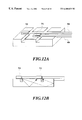
- FIGS. 12A and 12B are diagrams showing the construction of the optical module of an embodiment 9 of the present invention.
- FIGS. 13A and 13B are diagrams showing the construction of the optical module of an embodiment 10 of the present invention.
- FIGS. 14A and 14B are diagrams showing the construction of the optical module of an embodiment 11 of the present invention.
- FIG. 15 is a diagram showing changes in propagation loss at 1.3 to 1.5 ⁇ m wavelength region against electrical resistivity
- FIGS. 16A and 16B illustrate a modified example of the embodiment of FIGS. 14A and 14B, showing an embodiment 12;
- FIG. 17 is a further modified example of the embodiment of FIGS. 14A and 14B, showing an embodiment 13;
- FIG. 18 is a still further modified example of the embodiment of FIGS. 14A and 14B;
- FIG. 19 is a yet further modified example of the embodiment of FIGS. 14A and 14B, showing an embodiment 14;
- FIG. 20 is a diagram showing the construction of the optical module according to an embodiment 15 of the present invention.
- FIG. 21 is a perspective view showing an embodiment 16 of the present invention in the construction of FIG. 12A, the entire device being covered with a light absorbent resin;
- FIG. 22 is an exploded view showing parts of inside construction of FIG. 21;
- FIG. 23 shows a configuration of the optical module before providing the structure for suppressing leakage lights, wherein an optical waveguide such as an optical fiber is omitted for simplicity;
- FIG. 24 is a diagram showing an embodiment 17 in which a light absorbent resin is coated including a filter
- FIG. 25 is a diagram showing an embodiment 18 provided with caps as a light blocking body on respective optical devices and filter;
- FIG. 26 is a diagram showing an embodiment 19 in which the entire construction is covered with a single cap, rather than using discrete caps shown in FIG. 25;
- FIGS. 27A and 27B are diagrams showing the construction of a prior art optical module
- FIG. 28 is a plane diagram showing the construction of an example of prior art optical module provided with a light blocking area
- FIG. 29 is a plane diagram for explaining a leakage light generation circuit in a prior art optical module
- FIGS. 30A and 30B are diagrams for explaining the state of leakage lights entering the light receiving device in the optical module
- FIGS. 31A and 31B are diagrams for explaining a method for blocking lights transmitting through a cladding part
- FIGS. 32A to 32 C are diagrams for explaining a method using a wavelength selective filter.
- FIGS. 1A and 1B are diagrams showing the construction of the optical module according to an embodiment 1 of the present invention, in which FIG. 1A is a perspective view and FIG. 1B is a plane view.
- the optical module of the present embodiment is composed of an embedded type silica optical waveguide 2 comprising a cladding layer 2 b and a core 2 a formed on a silicon (Si) substrate 1 , a semiconductor chip of LD 30 disposed on the Si substrate 1 , a semiconductor chip of a monitor-receiver PD (which may be referred to simply as monitor PD) 32 and a semiconductor chip of a receiver PD 31 .
- the optical waveguide 2 is formed of two straight waveguides, and connected to ends of which are two optical fibers ( 4 a , 4 b ) with an optical fiber connection part 4 .
- the optical waveguide 2 is an embedded type optical waveguide 2 in which the core 2 a is embedded with the cladding layer 2 b having a sufficient thickness
- the “cladding layer of a sufficient thickness” means that the cladding layer is set thicker than a depth for the lights transmitting through the core 2 a to come out to the cladding layer 2 b , which normally requires a thickness equal to or greater than the core size.
- the three semiconductor devices ( 30 , 31 and 32 ) are all disposed on a recessed optical device mounting portion 15 formed by removing the optical waveguide 2 (core 2 a and cladding layer 2 b ) into a recessed form.
- the receiver PD 31 is disposed in such a manner that it is not positioned within the radiation angle of the backward output lights from the LD 30 .
- a characteristic feature of the present embodiment is that the rear side wall 150 of the recessed optical device mounting portion 15 is disposed obliquely.
- the rear side wall has an angle of about 80 degrees with respect to a perpendicular line of the optical axis of the backward output light from the LD 30 (about 10 degrees to a perpendicular line of the optical axis of backward output light from the LD 30 ).
- the backward output light from the LD 30 after being reflected by the rear side wall 150 of the recessed optical device mounting portion 15 , can be prevented from leaking into the receiver PD 31 .
- crosstalk light from the LD 30 to the receiver PD 31 was about ⁇ 30 dB.
- an optical module according to the prior art as shown in FIG. 2 was fabricated and the crosstalk light therein was measured.
- the LD 30 and the receiver PD 31 are disposed on the same recessed optical device mounting portion 15 , and the rear side wall 150 of the recessed optical device mounting portion 15 is almost perpendicular to the optical axis.
- crosstalk light from the LD 30 to the receiver PD 31 was about ⁇ 25 to ⁇ 27 dB. From the above comparison, the effect of the optical circuit construction of the present embodiment is apparent.
- the flat Si substrate 1 is patterned to etch an area other than a Si terrace (protruded portion) 50 to a depth of about 30 ⁇ m where the semiconductor chip of LD 30 , the semiconductor chip of monitor receiver PD 32 and the semiconductor chip of receiver PD 31 are to be mounted.
- a glass layer to be a lower cladding layer 51 is formed by a flame deposition method (FIG. 3 A).
- flat polishing is performed until the surface of the Si terrace 50 is exposed (FIG. 3 B). This surface becomes a level reference surface for the optical waveguide when the semiconductor chip of LD 30 , the semiconductor chip of monitor PD 32 and the semiconductor chip of receiver PD 31 are packaged.
- a height adjusting cladding layer (second lower cladding layer) 52 to be a height adjusting layer is formed.
- a core layer 53 is deposited to a thickness of about 7 ⁇ m (FIG. 3 C).
- an upper cladding layer 54 is deposited (FIG. 3 D).
- deposition of all of the cladding layers and the core layer is achieved by using the flame deposition method.
- electrode wirings for the LD 30 , the monitor receiver PD 32 and the receiver PD 31 are deposited, together with a mounting solder 55 (FIG. 3 E).
- FIG. 4 is a plane view showing a construction of the optical module according to an embodiment 2 of the present invention.
- the structure in the vicinity of the recessed optical device mounting portion 15 is same as embodiment 1.
- the module of the present embodiment differs from the embodiment 1 in that a light blocking area 20 is provided in front of the recessed optical device mounting portion 15 .
- the light blocking area 20 is provided to prevent forward output lights from the LD 30 from leaking into the optical fiber 4 b .
- a characteristic feature of the present embodiment resides in that a side wall 201 at the LD 30 side of the light blocking area 20 is slanted by an angle of about 70 degrees relative to the optical axis of the forward output lights of the LD 30 .
- the path of leakage lights caused by the forward output lights from the LD 30 reflected by the side wall 201 of the light blocking area 20 and leaking into the receiver PD 31 could be cut out.
- crosstalk light from the LD 30 to the receiver PD 31 was less than ⁇ 30 dB.
- an optical module according to the prior art as shown in FIG. 5 was fabricated and measured for crosstalk light.
- the rear side wall 150 of the recessed optical device mounting portion 15 and the side wall 201 of the light blocking area 20 are both disposed almost perpendicular to the optical axis of the LD 30 .
- crosstalk light from the LD 30 to the receiver PD 31 is decreased to about ⁇ 20 to ⁇ 24 dB, thus an effect of crosstalk light degradation due to the reflected lights is apparent. From the above comparison, the effect of the optical circuit construction of the present embodiment is apparent.
- FIG. 6 is a plane diagram showing the construction of an optical module according to an embodiment 3 of the present invention.
- the basic structure of the present embodiment is same as the above embodiment 1.
- the optical module of the present embodiment differs from the above embodiment 1 in the points that (1) the recessed optical device mounting portion 15 is filled with a transparent resin 5 for potting sealing, (2) the rear side wall 150 of the recessed optical device mounting portion 15 is set nearly perpendicular to the optical axis of rear output light from the LD 30 , (3) further, as a most characteristic structure, a light blocking area 21 is provided at the rear side of the recessed optical device mounting portion 15 which is filled with a black light absorbent substance, and its side wall 211 is set obliquely.
- the reason why the rear side wall 150 of the recessed optical device mounting portion 15 is not disposed obliquely is that since the recessed optical device mounting portion 15 is filled with the transparent resin 5 , reflection due to refractive index discontinuity at the side wall becomes negligibly small. However, in this case, reflection at an end of the optical waveguide is a problem, and the reflection therefrom generates a leakage light path. To prevent this, the light blocking area 21 is disposed at the rear of the recessed optical device mounting portion 15 . As a result, as the crosstalk light from the LD 30 to the receiver PD 31 , a value of about ⁇ 30 to ⁇ 33 dB was obtained.
- FIGS. 7A and 7B are diagrams showing the construction of an optical module according to an embodiment 4 of the present invention, in which FIG. 7A is a perspective diagram and FIG. 7B is a plane diagram.
- the optical module of the present embodiment comprises an embedded type silica optical waveguide 2 including a cladding layer 2 b and a core 2 a formed on a Si substrate 1 , and a semiconductor chip of LD 30 , a semiconductor chip of monitor receiver PD 32 and a semiconductor chip of receiver PD 31 , which are disposed on the Si substrate 1 .
- the optical waveguide 2 is formed of two straight waveguides, an end of which is connected with optical fibers 4 a and 4 b .
- the LD 30 and monitor receiver PD 32 are disposed on the recessed optical device mounting portion 15 formed by recessing the optical waveguide 2 (cladding layer 2 b ), and the receiver PD 31 is disposed on a recessed optical mounting portion 16 formed by recessing the optical waveguide 2 (cladding layer 2 b ). Further, a light blocking area 20 formed by removing the cladding layer 2 b other than the vicinity of the core 2 a is provided between the recessed optical device mounting portion 15 and the recessed optical device mounting portion 16 .
- the light blocking area 20 may be filled with an absorbent material in the inside, or an opaque metal film or the like may be formed on the side wall of the light blocking area 20 .
- a gold thin film was formed on the light blocking area 20 side wall.
- a characteristic of the present embodiment is that the LD 30 and the receiver PD 31 are disposed respectively on the different recessed optical device mounting portions ( 15 , 16 ), the light blocking area 20 is provided in between, and of the side walls, the side wall 201 closer to the output end of the LD 30 is disposed obliquely to have an angle of 70 degrees with respect to the optical axis of the forward output lights of the LD 30 .
- the rear side wall 150 of the recessed optical device mounting portion 15 for mounting the LD 30 is disposed obliquely.
- the component which is not coupled with the optical waveguide 2 is reflected by the side wall 201 of the light blocking area 20 .
- the side wall 201 has an angle of 70 degrees with respect to the optical axis of the forward output lights of the LD 30 , the light path is greatly changed after reflection, as a result, it can be prevented that the reflected light is coupled again with the LD 30 and the monitor receiver PD 32 .
- the rear side wall 150 of the recessed optical device mounting portion 15 is slanted, rearward output lights from the LD 30 can be prevented from leaking into the LD 30 and the monitor PD 32 .
- optical signals leaking from the LD 30 to the receiver PD 31 and the optical fiber 4 b at the receiver PD 31 side can be prevented by the light blocking area 20 .
- crosstalk light from the LD 30 to the receiver PD 31 was about ⁇ 35 dB. Further, crosstalk light from the LD 30 to the receiving optical fiber 4 b was ⁇ 50 dB.
- an optical transmitter and receiver module having the LD 30 and the receiver PD 31 when the receiver PD 31 is disposed at the front and the LD 30 at the rear, and a light blocking area having a slanted surface is disposed in between, two effects of leakage light suppression between devices and leakage light suppression to optical fibers can be provided by a single light blocking area.
- FIG. 8 is a plane diagram showing the construction of an optical module according to an embodiment 5 of the present invention.
- the LD 30 and the receiver PD 31 are disposed on different recessed optical device mounting portions ( 15 , 16 ).
- the present embodiment differs from the above embodiment 4 in that the LD 30 is disposed in front (that is, the optical fiber connection part 4 side) of the receiver PD 31 , and the recessed optical device mounting portions ( 15 , 16 ) are filled with a transparent resin for potting sealing.
- a light blocking area 21 and a light blocking area 20 are provided respectively in the front and rear of the recessed optical device mounting portion 15 on which the LD 30 is mounted.
- the side wall 211 and side wall 201 closer to the LD 30 of these light blocking areas ( 20 , 21 ) are set to be a curved surface and a slanted surface, respectively. Still further, in the present embodiment, the inside of the light blocking areas ( 20 , 21 ) is filled with a black filler for absorbing leakage lights.
- the side walls ( 201 , 211 ) of the light blocking areas ( 20 , 21 ) are formed to be a curved surface and a slanted surface, forward and rearward output lights of the LD 30 can be prevented, after being reflected by the side walls ( 201 , 211 ) of the light blocking areas ( 20 , 21 ), from coupling as return light again with the LD 30 , or from leaking into the optical fiber 4 b and the receiver PD 31 .
- crosstalk light from the LD 30 to the receiver PD 32 could be reduced to less than ⁇ 35 dB.
- FIG. 9 is a plane diagram showing the construction of an optical module according to an embodiment 6 of the present invention.
- reference numeral 34 indicates a 4-channel LD array
- 35 is an optical modulator array.
- These semiconductor optical devices and the optical fibers 4 a are respectively connected by an embedded type optical waveguide 2 .
- a light blocking area 22 is provided between the LD array 34 and the optical modulator array 35 , and its side wall is formed to be a slanted surface.
- FIG. 10 is a plane diagram showing the construction of an optical module according to an embodiment 7 of the present invention.
- the basic structure of the optical module of the present embodiment is almost the same as the above embodiment 6.
- the present embodiment differs from the above embodiment 6 in that the rear side wall 150 of the recessed optical device mounting portion 15 for mounting the LD array 34 is disposed obliquely.
- the return lights can be suppressed from the rear side wall 150 of the recessed optical device mounting portion 15 to the LDs themselves of the LD array 34 , a very stable operation of the LD array 34 is possible.
- FIG. 11 is a plane diagram showing the construction of an optical module according to an embodiment 8 of the present invention.
- the optical module of the present embodiment is composed of a 1.3 ⁇ m/1.55 ⁇ m wave multiplexing/demultiplexing circuit comprising a silica optical waveguide 2 and an interference film filter 10 , a 1.55 ⁇ m LD 30 semiconductor chip and its monitor PD 32 semiconductor chip disposed on the recessed optical device mounting portion 15 , and a 1.3 ⁇ m receiver PD 31 semiconductor chip disposed on the recessed optical device mounting portion 16 .
- a light blocking area 200 is provided, and to prevent reflection at an interface of the light blocking area 200 , a side wall 201 of the light blocking area 200 is disposed obliquely. Further, a rear side wall 202 of a light blocking area 200 is also slanted so that unnecessary reflected light at the interference film filter 10 does not return to the LD 30 .
- the rear side surface of the recessed optical device mounting portion 15 is slanted, and to prevent one part thereof from leaking into the optical fiber 4 a , a light blocking area 21 is provided at the rear of the recessed optical device mounting portion 15 , and its side wall 211 is also slanted to prevent reflection at an interface.
- light blocking areas ( 21 , 200 ) and the recessed optical device mounting portion 15 having slanted side surfaces were used, thereby achieving crosstalk light of less than ⁇ 45 dB from the LD 30 to the receiver PD 31 .
- FIGS. 12A and 12B shows an optical module in which a laser diode 30 as a light emitting device and a photodiode 31 as a light receiving device are disposed on a silicon substrate formed with V-grooves, and optical fibers 4 a and 4 b are connected to these devices.
- the components which are not optically coupled with the optical fiber as an optical waveguide, pass in the silicon substrate as indicated by the arrows in FIG. 12 B and reach the photodiode 31 to degrade reception characteristic of the module.
- a low-resistance substrate is used as the silicon substrate. Since the substrate size is 1 cm square, the resistance value, aiming at about 10 dB/cm, was set to about 0.005 ⁇ cm. This improved suppression of an undesirable optical crosstalk in the optical module by about 10 dB.
- FIGS. 13A and 13B are diagrams for explaining an embodiment 10 of the optical module in which an optical waveguide core part 2 a is formed on a silica glass substrate 10 to dispose a light emitting device 30 and a light receiving device 31 .
- the optical waveguide comprises a core part 2 a and a cladding part 2 b differing in refractive index, and the light emitting device 30 and the light receiving device 31 are disposed on respective recesses formed in the cladding part 2 b so that they are coupled with the core part 2 a .
- an area 14 containing a large amount of metal is formed in a part other than the vicinity of the core part 2 a of the optical waveguide.
- the vicinity of the core part 2 a generally indicates about twice as long as a mode field diameter which is an area confining lights of the optical waveguide, in this case means a part of about four times as wide as the optical waveguide width.
- Co or the like is effective (Kanayama et al., “Characteristics of SC Type Fixed Attenuator using Metal Doped Fiber”, 1994 Spring Conference of the Society of Electronic Information Communications, C-347 In Japanese).
- the attenuation is preferably about 3 dB/cm.
- metal doping to the rear part of the light emitting device 30 is not shown in FIG. 13A, when rear radiation is a problem, a metal-added area is provided also at the rear. Further, a contour of the metal-added area 14 is expressly shown in FIG. 13A for better understanding, however, in practice, it is convenient to pattern a metal film and use thermal diffusion, and, by this method the boundary of the metal-added area 14 becomes unclear. Still further, it is not always uniform also in the height direction. However, it is necessary to arrange and that the diffused metal does not reach the core part 2 a of the optical waveguide and its periphery.
- a silica glass substrate is used, however, alternatively, for example, a semiconductor substrate such as Si substrate or a ceramic substrate such as alumina may be used.
- FIGS. 14A and 14B are diagrams for explaining an embodiment 11 of the optical module according to the present invention, in which silica glass optical waveguide core part 2 a and cladding part 2 b are formed on a Si substrate 13 , and a light emitting device 30 and a light receiving device 31 are disposed.
- the module structure of the present embodiment differs from the embodiment 10 in that the substrate is Si.
- transmission of stray lights is suppressed utilizing a property of Si that an absorption coefficient rapidly increases with increasing conductive carrier density (see, for example, R. D. Soref et al., “Electrooptical Effects in Silicon”, IEEE J. Quantum Electron., vol. QE-23, No. 1 (1987).
- FIG. 15 shows changes in propagation loss in 1.3 to 1.5 ⁇ m wavelength regions against electrical resistivity. It can be seen from the Figure that when an absorption of more than 1 dB/cm is expected, an electrical resistivity of less than about 0.1 ⁇ cm may be sufficient. In the present embodiment, the electrical resistivity was set to about 0.01 ⁇ cm aiming at about 5 dB/cm to attenuate stray lights leaking into the Si substrate 13 . In this case, since the module size is about 2 cm, by the above arrangement, noise due to stray lights transmitting in the Si substrate could be suppressed by about 10 dB. As described, in the optical waveguide using a semiconductor substrate, stray lights leaking to the substrate can be efficiently reduced by adjusting the carrier density.
- FIGS. 16A and 16B shows a module, which, in the optical module of embodiment 11, the lower side of the light emitting device is set to a low resistance of 0.005 ⁇ cm and the lower side of the light receiving device is set to a high resistance of 1 k ⁇ cm.
- Local resistance distribution can be simply achieved by a typical semiconductor process. For example, local resistivity can be easily changed by locally implanting ions by a photolithography process and an ion implantation process.
- a low-resistance part 6 of about 0.01 ⁇ cm was formed.
- the silicon substrate part in the vicinity of the light receiving device is a high resistance area 7 as shown in FIGS. 16A and 16B, degradation in optical module characteristics associated with the low resistance can be suppressed.
- the absorption area is about 1 cm in width, which provided an optical crosstalk in the optical module of about 5 dB.
- FIG. 17, as in the case of FIG. 14A, is a diagram for explaining an embodiment 13 of an optical module according to the present invention, in which silica glass optical waveguide core part 2 a and cladding part 2 b are formed on a Si substrate 13 . and a light emitting device 30 and a light receiving device 31 are disposed. Since, due to the property of Si, a non-doped substrate is transparent to the light of 1.3 ⁇ m and 1.55 ⁇ m as communication wavelengths, stray lights leaking into Si transmit almost without propagation loss and repeat reflections at a side or bottom surface of the module to enter the light receiving device 31 , resulting in noises.
- grooves 15 are formed on the bottom surface of the Si substrate 13 to block transmission of light in Si (FIG. 17 ), or fine irregularities are formed on the bottom surface or the bottom and side surfaces of the Si substrate to diffuse reflected lights transmitted in Si so that they do not enter the light receiving device 31 (FIG. 18 ). In the latter case, it is even further effective to form fine irregularities also on the surface of the cladding part 2 b . Formation of irregularities can be performed using plasma etching.
- noise considered to be originated in stray lights could be suppressed by about 10 dB.
- the structure provided with grooves on the substrate back surface and the structure with roughened surface stray lights can be efficiently reduced. Further, since, by the structure provided with grooves formed on the substrate back surface, optical noise can be suppressed, and impedance can be increased between the light emitting device and the light receiving device of the substrate, an effect to suppress an electrical crosstalk is also obtained.
- FIG. 19, as in the case of FIG. 14A, is a diagram for explaining an embodiment 14 of an optical module according to the present invention, in which silica glass optical waveguide core part 2 a and cladding part 2 b are formed on a Si substrate 13 . and a light emitting device 30 and a light receiving device 31 are disposed.
- a resin layer 17 containing a light absorbent on the periphery of the optical module, stray lights are absorbed by the surface of the module, thereby suppressing reflection of stray lights at the surface.
- a black epoxy resin containing a filler is used as the resin, which is coated on the periphery of the optical module.
- epoxy resin is about 1.5 in refractive index
- silica is 1.5
- Si is about 3.5
- stray lights can be suppressed at the interface between the resin and Si by about 1.4 dB compared with the case of air, and almost perfectly at the interface between the resin and silica waveguide cladding.
- the resin layer 17 containing a light absorbent on the periphery of the optical module, noise considered to be due to stray lights can be efficiently suppressed.
- 18 indicates a portion provided with electrical wiring and a solder layer for mounting the light receiving device 31
- other hatched portions 19 are those on which a portion blocking layer is formed.
- a light blocking layer 19 comprising a metal is provided on the periphery of the portion where the light emitting device 30 and the light receiving device 31 are mounted.
- a light blocking layer is formed to block stray lights from below and lateral direction of the light receiving device 30 .
- a light blocking layer may be formed to block entrance of lights not coupled with the optical waveguide core 2 a into the cladding 2 b or the substrate 13 .
- the above structure is not necessarily provided on the optical waveguide substrate or cladding part, instead, the part of the light receiving device other than receiving lights from the optical waveguide may be covered.
- the light blocking layer to block lights may be other than a metal film.
- use of a light absorbing coating film can be expected to provide an effect to suppress diffuse reflection of lights. As described above, by using a light blocking layer, stray lights reaching the light receiving device can be efficiently suppressed.
- FIG. 21 shows the optical module construction of an embodiment 16 according to the third aspect of the present invention.
- the structure according to the present embodiment is based on the optical module of the embodiment of FIGS. 12A and 12B, a resin as a light absorbent is coated on the substrate surface of the module to cover the optical devices and optical fibers.
- a resin as a light absorbent is coated on the substrate surface of the module to cover the optical devices and optical fibers.
- FIG. 22 the part where the resin is applied is removed.
- the structure is described in detail in the following.
- the periphery of optical devices is all coated with a transparent resin 9 so that there is no loss in coupling with the optical fibers.
- a transparent resin 9 it is important that the transparent resin is divided between two devices.
- the light absorbent 8 when the light absorbent 8 is coated on the substrate surface, the light absorbent 8 can flow into the divided part of the transparent resin 9 , thereby blocking leakage lights from the light emitting device 30 passing over the substrate and reaching the light receiving device 31 .
- FIGS. 23 and 24 show the circuit construction of an optical module according to an embodiment 17.
- the optical waveguide is not shown since it is almost unrelated to the present embodiment.
- the basic construction of the optical circuit is same as in FIGS. 32A and 32B.
- the filter 10 in addition to the light emitting device 30 and the light receiving device 31 .
- Leakage lights (as indicated by arrows in FIG. 32C) emitted from the light emitting device are strongly scattered by the filter part to transmit from above the waveguide substrate to the light receiving device, resulting in degraded reception characteristics.
- the substrate surface including the optical filter 10 is coated with the light absorbent.
- Reference numeral 21 indicates a filter fixing adhesive.
- FIG. 25 shows a construction in which each of optical devices 30 and 31 and an optical filter 10 are covered with a light blocking cap 81 as a light blocking body instead of the light absorbent.
- the caps are each fixed with solder on the substrate, and provide a local sealing function.
- the material of the cap is airtight sintered alumina which does not transmit light.
- As another material one which is surrounded by a resin or glass may be used.
- the three areas are covered with different caps, however, alternatively, when capped, a single cap 81 having walls in the inside for separating respective devices to suppress leakage lights may be used.
- the module when the module is subjected to a humidity/thermal test, it was found to withstand a temperature of 85° C. and a humidity of 90% for more than 7000 hours, thus the cap providing airtightness and sealing effects.
Landscapes
- Physics & Mathematics (AREA)
- General Physics & Mathematics (AREA)
- Optics & Photonics (AREA)
- Optical Integrated Circuits (AREA)
- Optical Couplings Of Light Guides (AREA)
- Semiconductor Lasers (AREA)
Applications Claiming Priority (6)
| Application Number | Priority Date | Filing Date | Title |
|---|---|---|---|
| JP26118197A JPH11101926A (ja) | 1997-09-26 | 1997-09-26 | 光モジュール |
| JP9-261181 | 1997-09-26 | ||
| JP261181/1997 | 1997-09-26 | ||
| JP10054998A JPH11248954A (ja) | 1998-03-06 | 1998-03-06 | 光ハイブリッドモジュール |
| JP54998/1998 | 1998-03-06 | ||
| JP10-054998 | 1998-03-06 |
Publications (2)
| Publication Number | Publication Date |
|---|---|
| US20020001427A1 US20020001427A1 (en) | 2002-01-03 |
| US6480639B2 true US6480639B2 (en) | 2002-11-12 |
Family
ID=26395826
Family Applications (1)
| Application Number | Title | Priority Date | Filing Date |
|---|---|---|---|
| US09/158,090 Expired - Fee Related US6480639B2 (en) | 1997-09-26 | 1998-09-22 | Optical module |
Country Status (3)
| Country | Link |
|---|---|
| US (1) | US6480639B2 (de) |
| EP (1) | EP0905536B1 (de) |
| DE (1) | DE69827898T2 (de) |
Cited By (35)
| Publication number | Priority date | Publication date | Assignee | Title |
|---|---|---|---|---|
| US20020102044A1 (en) * | 2001-01-08 | 2002-08-01 | Bookham Technologies Plc | Optical circuit device |
| US20020141709A1 (en) * | 2001-03-28 | 2002-10-03 | Shin Ki Chul | Small-formed optical module |
| US20020182631A1 (en) * | 1999-12-17 | 2002-12-05 | Eveline Schurmann-Mader | Flow cell array and the utilization thereof for multianalyte determination |
| US20030044119A1 (en) * | 2001-08-28 | 2003-03-06 | Takashi Sasaki | Optical waveguide module |
| US20030091303A1 (en) * | 2001-01-26 | 2003-05-15 | Nec Corporation | Optical transmitter-receiver module suitable for reducing crosstalk |
| US20030152338A1 (en) * | 2002-02-08 | 2003-08-14 | Yoshiki Kuhara | Parallel light emitting device - photosensitive device module |
| US20030190124A1 (en) * | 2002-04-03 | 2003-10-09 | Yoshiki Kuhara | Multichannel optical communications module |
| US20030202748A1 (en) * | 2002-04-24 | 2003-10-30 | Gordon Gary B. | Tri-state optical sytems and methods |
| US6684012B2 (en) * | 2000-09-13 | 2004-01-27 | Nec Corporation | Optical communication module and process for producing the same |
| US6707838B2 (en) * | 2001-05-28 | 2004-03-16 | Fuji Photo Film Co., Ltd. | Stray light cutting structure for optical device |
| US20040057673A1 (en) * | 2002-09-16 | 2004-03-25 | Kuzma Andrew J. | Integrated selectable waveguide for optical networking components |
| US20040151460A1 (en) * | 2001-05-30 | 2004-08-05 | Daniel Kitcher | Deep trenches for optical and electrical isolation |
| US6783283B2 (en) * | 2001-04-27 | 2004-08-31 | The Furukawa Electric Co., Ltd. | Optical connector for coupling optical signals to optical devices |
| US6789959B1 (en) | 2003-02-27 | 2004-09-14 | Xilinx, Inc. | Fiber optic integrated circuit package using micromirrors |
| US6810057B1 (en) * | 1999-11-25 | 2004-10-26 | Matsushita Electric Industrial Co., Ltd. | Semiconductor device and optical pickup device |
| US20040247230A1 (en) * | 2003-06-09 | 2004-12-09 | Oh-Dal Kwon | Optical hybrid module and manufacturing method thereof |
| US6945712B1 (en) | 2003-02-27 | 2005-09-20 | Xilinx, Inc. | Fiber optic field programmable gate array integrated circuit packaging |
| US7050678B1 (en) * | 1998-08-28 | 2006-05-23 | Fujikura Ltd. | Optical module, optical element attachment method, and receptacle-fitted optical module |
| US20060110089A1 (en) * | 2002-08-30 | 2006-05-25 | Junichiro Ichikawa | Optical modulator |
| US7142740B2 (en) | 2004-09-09 | 2006-11-28 | Electronics And Telecommunications Research Institute | Planar lightwave circuit type optical transceiver module |
| US20070081755A1 (en) * | 2005-03-31 | 2007-04-12 | Sumitomo Osaka Cement Co., Ltd. | Optical modulator |
| US20080193141A1 (en) * | 2006-10-02 | 2008-08-14 | Takuya Shinoda | Optical transmitter-receiver module |
| US7492992B1 (en) * | 2003-08-08 | 2009-02-17 | Neophotonics Corporation | Bi-directional PLC transceiver device |
| US20090072419A1 (en) * | 2007-09-13 | 2009-03-19 | Samsung Electro-Mechanics Co., Ltd. | Method of manufacturing optical waveguide and method of manufacturing package board |
| US20090297086A1 (en) * | 2006-03-30 | 2009-12-03 | Sumitomo Osaka Cement Co., Ltd. | Light Modulation Device |
| US7708945B1 (en) * | 1999-08-13 | 2010-05-04 | Bayer Technology Services Gmbh | Device and method for determining multiple analytes |
| US20100322569A1 (en) * | 2007-06-28 | 2010-12-23 | Nippon Telegraph And Telephone Corporation | Optical module |
| US20110052208A1 (en) * | 2009-08-31 | 2011-03-03 | Kabushiki Kaisha Toshiba | Optoelectronic wiring film and optoelectronic wiring module |
| US20110110629A1 (en) * | 2008-07-30 | 2011-05-12 | Mitsuru Nagano | Planar optical waveguide |
| US20120057880A1 (en) * | 2010-09-06 | 2012-03-08 | Araceli Ruiz | Cross-talk reduction in a bidirectional optoelectronic device |
| US8861970B2 (en) | 2010-04-28 | 2014-10-14 | Hoya Corporation Usa | Cross-talk reduction in a bidirectional optoelectronic device |
| US20140355932A1 (en) * | 2012-01-19 | 2014-12-04 | Ixblue | Integrated optical circuit with traversing attentuation zone |
| US20150205043A1 (en) * | 2009-11-26 | 2015-07-23 | Ntt Electronics Corporation | Optical waveguide device and module |
| US20210218217A1 (en) * | 2019-03-14 | 2021-07-15 | Hisense Broadband Multimedia Technologies Co., Ltd. | Optical transmission module, optical transmission-reception module and optical module |
| US20220373737A1 (en) * | 2019-07-09 | 2022-11-24 | Nippon Telegraph And Telephone Corporation | Optical Multiplexing Circuit |
Families Citing this family (22)
| Publication number | Priority date | Publication date | Assignee | Title |
|---|---|---|---|---|
| US6085005A (en) * | 1998-02-26 | 2000-07-04 | Lucent Technologies, Inc. | Optical assembly with a coated component |
| JP2001133645A (ja) * | 1999-11-04 | 2001-05-18 | Nec Corp | 光導波路モジュールにおける迷光遮光構造及びそれを用いた光送受信モジュール |
| US6693712B1 (en) * | 1999-12-02 | 2004-02-17 | Teraconnect, Inc. | High rate optical correlator implemented on a substrate |
| AU3167001A (en) * | 2000-01-17 | 2001-07-31 | Corning O.T.I. S.P.A. | Attenuator integrated with modulator and transmitting module for wdm system using the same |
| JP2001210841A (ja) * | 2000-01-24 | 2001-08-03 | Sumitomo Electric Ind Ltd | 光通信装置 |
| JP2001305365A (ja) * | 2000-04-25 | 2001-10-31 | Nec Corp | 光導波路モジュールにおける迷光の遮光構造 |
| CA2377116A1 (en) * | 2001-08-28 | 2003-02-28 | Sumitomo Electric Industries, Ltd. | Optical waveguide module |
| US6924510B2 (en) | 2002-05-06 | 2005-08-02 | Intel Corporation | Silicon and silicon/germanium light-emitting device, methods and systems |
| KR100460840B1 (ko) * | 2002-08-09 | 2004-12-09 | 한국전자통신연구원 | 광 및 전기 크로스톡을 동시에 억제할 수 있는 광모듈 |
| EP1396741A1 (de) * | 2002-09-04 | 2004-03-10 | Avanex Corporation | Streulichtunterdrückungsstrukturen mit einem Wellenleiter und tief unter einem Winkel geätzten und mit einem Absorbermaterial gefüllten Gräben |
| JP2007187793A (ja) * | 2006-01-12 | 2007-07-26 | Nec Corp | 光モジュール |
| JP5497996B2 (ja) * | 2008-05-26 | 2014-05-21 | 日本電信電話株式会社 | 導波路型デバイスにおける導波路終端方法 |
| JP2013003224A (ja) * | 2011-06-14 | 2013-01-07 | Shinko Electric Ind Co Ltd | 光導波路及びその製造方法と光導波路装置 |
| US8777497B2 (en) * | 2011-10-06 | 2014-07-15 | Electronics And Telecommunications Research Institute | Bidirectional optical transceiver module |
| JP5571741B2 (ja) * | 2012-06-19 | 2014-08-13 | 日本電信電話株式会社 | 光モジュール |
| JP6186654B2 (ja) | 2013-06-24 | 2017-08-30 | 華為技術有限公司Huawei Technologies Co.,Ltd. | 光モジュール及び光ネットワークシステム |
| WO2015008451A1 (ja) * | 2013-07-18 | 2015-01-22 | 日本電気株式会社 | 光送受信モジュール |
| US9508879B2 (en) * | 2013-10-23 | 2016-11-29 | Alcatel Lucent | Detector device |
| AU2016391182B2 (en) * | 2016-02-02 | 2019-07-25 | Huawei Technologies Co., Ltd. | Single optical fiber bi-directional sub-assembly |
| US10444445B2 (en) * | 2017-02-10 | 2019-10-15 | Ciena Corporation | Optically isolated photodiode for high sensitivity application |
| US10877213B2 (en) * | 2018-06-20 | 2020-12-29 | Hisense Broadband Multimedia Technologies Co., Ltd. | Optical module |
| EP4049074A4 (de) | 2019-10-25 | 2023-11-15 | CommScope Technologies LLC | Integrierte optische wellenlängenmultiplexvorrichtungen |
Citations (6)
| Publication number | Priority date | Publication date | Assignee | Title |
|---|---|---|---|---|
| US4210923A (en) * | 1979-01-02 | 1980-07-01 | Bell Telephone Laboratories, Incorporated | Edge illuminated photodetector with optical fiber alignment |
| JPS61174790A (ja) * | 1985-01-30 | 1986-08-06 | Oki Electric Ind Co Ltd | 半導体レ−ザダイオ−ド装置 |
| US4926545A (en) * | 1989-05-17 | 1990-05-22 | At&T Bell Laboratories | Method of manufacturing optical assemblies |
| US4974041A (en) * | 1986-08-25 | 1990-11-27 | Hughes Aircraft Company | Integrated circuit structure with multiple common planes and method of forming the same |
| JPH095548A (ja) | 1995-06-19 | 1997-01-10 | Nippon Telegr & Teleph Corp <Ntt> | 光導波回路 |
| US5900763A (en) * | 1994-10-11 | 1999-05-04 | Motorola, Inc. | Circuit and method of reducing cross-talk in an integrated circuit substrate |
Family Cites Families (10)
| Publication number | Priority date | Publication date | Assignee | Title |
|---|---|---|---|---|
| DE58904033D1 (de) * | 1988-02-19 | 1993-05-19 | Siemens Ag | Isoliereinrichtung zum optischen isolieren integrierter komponenten. |
| GB2231683A (en) * | 1989-05-12 | 1990-11-21 | Plessey Co Plc | A semi-conductor waveguide arrangement and method of fabrication therefof |
| US4969712A (en) * | 1989-06-22 | 1990-11-13 | Northern Telecom Limited | Optoelectronic apparatus and method for its fabrication |
| US5321779A (en) * | 1992-11-06 | 1994-06-14 | The Charles Stark Draper Laboratory, Inc. | Optical substrate with light absorbing segments |
| JPH06186451A (ja) * | 1992-12-16 | 1994-07-08 | Nec Eng Ltd | 光導波路デバイス |
| JP2981371B2 (ja) * | 1993-07-19 | 1999-11-22 | シャープ株式会社 | 光結合装置 |
| US5475772A (en) * | 1994-06-02 | 1995-12-12 | Honeywell Inc. | Spatial filter for improving polarization extinction ratio in a proton exchange wave guide device |
| SE506654C2 (sv) * | 1994-09-16 | 1998-01-26 | Sitek Electro Optics Ab | Positionskänslig fotodetektor med eliminerad inverkan av ströljus |
| JPH09159854A (ja) * | 1995-12-04 | 1997-06-20 | Hitachi Cable Ltd | 光伝送モジュール及びその製造方法 |
| FR2748573B1 (fr) * | 1996-05-10 | 1998-06-05 | Commissariat Energie Atomique | Filtre en optique integree |
-
1998
- 1998-09-22 US US09/158,090 patent/US6480639B2/en not_active Expired - Fee Related
- 1998-09-24 EP EP98118137A patent/EP0905536B1/de not_active Expired - Lifetime
- 1998-09-24 DE DE69827898T patent/DE69827898T2/de not_active Expired - Lifetime
Patent Citations (6)
| Publication number | Priority date | Publication date | Assignee | Title |
|---|---|---|---|---|
| US4210923A (en) * | 1979-01-02 | 1980-07-01 | Bell Telephone Laboratories, Incorporated | Edge illuminated photodetector with optical fiber alignment |
| JPS61174790A (ja) * | 1985-01-30 | 1986-08-06 | Oki Electric Ind Co Ltd | 半導体レ−ザダイオ−ド装置 |
| US4974041A (en) * | 1986-08-25 | 1990-11-27 | Hughes Aircraft Company | Integrated circuit structure with multiple common planes and method of forming the same |
| US4926545A (en) * | 1989-05-17 | 1990-05-22 | At&T Bell Laboratories | Method of manufacturing optical assemblies |
| US5900763A (en) * | 1994-10-11 | 1999-05-04 | Motorola, Inc. | Circuit and method of reducing cross-talk in an integrated circuit substrate |
| JPH095548A (ja) | 1995-06-19 | 1997-01-10 | Nippon Telegr & Teleph Corp <Ntt> | 光導波回路 |
Non-Patent Citations (4)
| Title |
|---|
| Kanayama et al., "Characteristic of SC Type Fixed Attenuator using Metal Doped Fiber", 1994 Spring Conference of the Society of Electronic Information Communications, C-347, English and Japanese translation. |
| R.D. Soref et al., Electrooptical Effects in Silicon, IEEE J. Quantum Electron., vol. QE-23, No. 1 (1987). |
| Yamada et al., "Application of Planar Lightwave Circuit Platform to Hybrid Integrated Optical WDM Transmitter/Receiver Module", Electronic Letters, vol. 31, No. 16 (Aug. 3, 1995). |
| Yamada et al., "Filter-type WDM Transceiver Optical Circuit Using PLC Platform", Preprint of Proceedings for 1996 Spring Conference of Society of Electronic Communicaitons. |
Cited By (62)
| Publication number | Priority date | Publication date | Assignee | Title |
|---|---|---|---|---|
| US7050678B1 (en) * | 1998-08-28 | 2006-05-23 | Fujikura Ltd. | Optical module, optical element attachment method, and receptacle-fitted optical module |
| US7708945B1 (en) * | 1999-08-13 | 2010-05-04 | Bayer Technology Services Gmbh | Device and method for determining multiple analytes |
| US20100227773A1 (en) * | 1999-08-13 | 2010-09-09 | Andreas Peter Abel | Device and method for determining multiple analytes |
| US7927868B2 (en) | 1999-08-13 | 2011-04-19 | Bayer Technology Services Gmbh | Device and method for determining multiple analytes |
| US6810057B1 (en) * | 1999-11-25 | 2004-10-26 | Matsushita Electric Industrial Co., Ltd. | Semiconductor device and optical pickup device |
| US7678565B2 (en) | 1999-12-17 | 2010-03-16 | Bayer Technology Services Gmbh | Flow cell array and the utilization thereof for multianalyte determination |
| US7358079B2 (en) * | 1999-12-17 | 2008-04-15 | Bayer Technology Services Gmbh | Flow cell array and the utilization thereof for multianalyte determination |
| US20020182631A1 (en) * | 1999-12-17 | 2002-12-05 | Eveline Schurmann-Mader | Flow cell array and the utilization thereof for multianalyte determination |
| US20100130370A1 (en) * | 1999-12-17 | 2010-05-27 | Eveline Schurmann-Mader | Flow cell array and the utilization thereof for multianalyte determination |
| US8053225B2 (en) | 1999-12-17 | 2011-11-08 | Bayer Technology Services Gmbh | Flow cell array and the utilization thereof for multianalyte determination |
| US6684012B2 (en) * | 2000-09-13 | 2004-01-27 | Nec Corporation | Optical communication module and process for producing the same |
| US20020102044A1 (en) * | 2001-01-08 | 2002-08-01 | Bookham Technologies Plc | Optical circuit device |
| US6663295B2 (en) * | 2001-01-26 | 2003-12-16 | Nec Corporation | Optical transmitter-receiver module suitable for reducing crosstalk |
| US20030091303A1 (en) * | 2001-01-26 | 2003-05-15 | Nec Corporation | Optical transmitter-receiver module suitable for reducing crosstalk |
| US20020141709A1 (en) * | 2001-03-28 | 2002-10-03 | Shin Ki Chul | Small-formed optical module |
| US6783283B2 (en) * | 2001-04-27 | 2004-08-31 | The Furukawa Electric Co., Ltd. | Optical connector for coupling optical signals to optical devices |
| US6707838B2 (en) * | 2001-05-28 | 2004-03-16 | Fuji Photo Film Co., Ltd. | Stray light cutting structure for optical device |
| US20040151460A1 (en) * | 2001-05-30 | 2004-08-05 | Daniel Kitcher | Deep trenches for optical and electrical isolation |
| US20030044119A1 (en) * | 2001-08-28 | 2003-03-06 | Takashi Sasaki | Optical waveguide module |
| US20030152338A1 (en) * | 2002-02-08 | 2003-08-14 | Yoshiki Kuhara | Parallel light emitting device - photosensitive device module |
| US6863449B2 (en) * | 2002-02-08 | 2005-03-08 | Sumitomo Electric Industries, Ltd. | Parallel light emitting device—photosensitive device module |
| US20050163420A1 (en) * | 2002-04-03 | 2005-07-28 | Sumitomo Electric Industries, Ltd. | Multichannel optical communications module |
| US20030190124A1 (en) * | 2002-04-03 | 2003-10-09 | Yoshiki Kuhara | Multichannel optical communications module |
| US7153037B2 (en) | 2002-04-03 | 2006-12-26 | Sumitomo Electric Industries, Ltd. | Multichannel optical communications module |
| US6882763B2 (en) * | 2002-04-03 | 2005-04-19 | Sumitomo Electric Industries, Ltd. | Multichannel optical communications module |
| US6956996B2 (en) * | 2002-04-24 | 2005-10-18 | Agilent Technologies, Inc. | Tri-state optical systems and methods |
| US20030202748A1 (en) * | 2002-04-24 | 2003-10-30 | Gordon Gary B. | Tri-state optical sytems and methods |
| US20060110089A1 (en) * | 2002-08-30 | 2006-05-25 | Junichiro Ichikawa | Optical modulator |
| US7310453B2 (en) * | 2002-08-30 | 2007-12-18 | Sumitomo Osaka Cement Co., Ltd. | Optical modulator |
| US6879765B2 (en) * | 2002-09-16 | 2005-04-12 | Intel Corporation | Integrated selectable waveguide for optical networking components |
| US20040057673A1 (en) * | 2002-09-16 | 2004-03-25 | Kuzma Andrew J. | Integrated selectable waveguide for optical networking components |
| US6789959B1 (en) | 2003-02-27 | 2004-09-14 | Xilinx, Inc. | Fiber optic integrated circuit package using micromirrors |
| US6945712B1 (en) | 2003-02-27 | 2005-09-20 | Xilinx, Inc. | Fiber optic field programmable gate array integrated circuit packaging |
| US7181098B2 (en) * | 2003-06-09 | 2007-02-20 | Samsung Electronics Co., Ltd. | Optical hybrid module and manufacturing method thereof |
| US20040247230A1 (en) * | 2003-06-09 | 2004-12-09 | Oh-Dal Kwon | Optical hybrid module and manufacturing method thereof |
| US7492992B1 (en) * | 2003-08-08 | 2009-02-17 | Neophotonics Corporation | Bi-directional PLC transceiver device |
| US7142740B2 (en) | 2004-09-09 | 2006-11-28 | Electronics And Telecommunications Research Institute | Planar lightwave circuit type optical transceiver module |
| US7409114B2 (en) * | 2005-03-31 | 2008-08-05 | Sumitomo Osaka Cement Co., Ltd. | Optical modulator |
| US20070081755A1 (en) * | 2005-03-31 | 2007-04-12 | Sumitomo Osaka Cement Co., Ltd. | Optical modulator |
| US20090297086A1 (en) * | 2006-03-30 | 2009-12-03 | Sumitomo Osaka Cement Co., Ltd. | Light Modulation Device |
| US8031983B2 (en) | 2006-03-30 | 2011-10-04 | Sumitomo Osaka Cement Co., Ltd. | Light modulation device |
| US20080193141A1 (en) * | 2006-10-02 | 2008-08-14 | Takuya Shinoda | Optical transmitter-receiver module |
| US20100322569A1 (en) * | 2007-06-28 | 2010-12-23 | Nippon Telegraph And Telephone Corporation | Optical module |
| US8545111B2 (en) * | 2007-06-28 | 2013-10-01 | Nippon Telegraph And Telephone Corporation | Optical module |
| US20090072419A1 (en) * | 2007-09-13 | 2009-03-19 | Samsung Electro-Mechanics Co., Ltd. | Method of manufacturing optical waveguide and method of manufacturing package board |
| US8048324B2 (en) * | 2007-09-13 | 2011-11-01 | Samsung Electro-Mechanics Co., Ltd. | Method of manufacturing optical waveguide and method of manufacturing package board |
| US8615146B2 (en) * | 2008-07-30 | 2013-12-24 | Ntt Electronics Corporation | Planar optical waveguide |
| US20110110629A1 (en) * | 2008-07-30 | 2011-05-12 | Mitsuru Nagano | Planar optical waveguide |
| US20110052208A1 (en) * | 2009-08-31 | 2011-03-03 | Kabushiki Kaisha Toshiba | Optoelectronic wiring film and optoelectronic wiring module |
| US9684129B2 (en) * | 2009-11-26 | 2017-06-20 | Ntt Electronics Corporation | Optical waveguide device and module |
| US20150205043A1 (en) * | 2009-11-26 | 2015-07-23 | Ntt Electronics Corporation | Optical waveguide device and module |
| US10126502B2 (en) | 2009-11-26 | 2018-11-13 | Ntt Electronics Corporation | Optical waveguide device and module |
| US8861970B2 (en) | 2010-04-28 | 2014-10-14 | Hoya Corporation Usa | Cross-talk reduction in a bidirectional optoelectronic device |
| US8750712B2 (en) * | 2010-09-06 | 2014-06-10 | Hoya Corporation Usa | Cross-talk reduction in a bidirectional optoelectronic device |
| US9178622B2 (en) | 2010-09-06 | 2015-11-03 | Hoya Corporation Usa | Cross-talk reduction in a bidirectional optoelectronic device |
| US20120057880A1 (en) * | 2010-09-06 | 2012-03-08 | Araceli Ruiz | Cross-talk reduction in a bidirectional optoelectronic device |
| US20140355932A1 (en) * | 2012-01-19 | 2014-12-04 | Ixblue | Integrated optical circuit with traversing attentuation zone |
| US9239430B2 (en) * | 2012-01-19 | 2016-01-19 | Ixblue | Integrated optical circuit with traversing attentuation zone |
| US20210218217A1 (en) * | 2019-03-14 | 2021-07-15 | Hisense Broadband Multimedia Technologies Co., Ltd. | Optical transmission module, optical transmission-reception module and optical module |
| US12272928B2 (en) * | 2019-03-14 | 2025-04-08 | Hisense Broadband Multimedia Technologies Co., Ltd. | Optical transmission module, optical transmission-reception module and optical module |
| US20220373737A1 (en) * | 2019-07-09 | 2022-11-24 | Nippon Telegraph And Telephone Corporation | Optical Multiplexing Circuit |
| US12072528B2 (en) * | 2019-07-09 | 2024-08-27 | Nippon Telegraph And Telephone Corporation | Optical multiplexing circuit |
Also Published As
| Publication number | Publication date |
|---|---|
| EP0905536B1 (de) | 2004-12-01 |
| EP0905536A2 (de) | 1999-03-31 |
| DE69827898T2 (de) | 2005-12-22 |
| DE69827898D1 (de) | 2005-01-05 |
| EP0905536A3 (de) | 2002-11-13 |
| US20020001427A1 (en) | 2002-01-03 |
Similar Documents
| Publication | Publication Date | Title |
|---|---|---|
| US6480639B2 (en) | Optical module | |
| JP3792040B2 (ja) | 双方向光半導体装置 | |
| US6546171B2 (en) | Structure for shielding stray light in optical waveguide module | |
| CN100437185C (zh) | 光电复合组件 | |
| US6904209B2 (en) | Optical communication module | |
| JPH11248954A (ja) | 光ハイブリッドモジュール | |
| EP1028339B1 (de) | Licht sendendes/empfangendes Modul | |
| US6547451B1 (en) | Optical communications module and method for mounting optical communications module | |
| KR100484998B1 (ko) | 양방향 광 전송 장치 | |
| CA2331577A1 (en) | Optical communication device | |
| US7024079B2 (en) | Optical waveguide module | |
| US6908235B2 (en) | Sub-mount and optical receiver using the same | |
| EP1195632A2 (de) | Photodiodenzeilen- Vorrichtung, ein Photodiodenmodul, und eine Anordnung zum Verbinden des Photodiodenmoduls mit einem optischen Verbinder | |
| JP2000075155A (ja) | 光モジュール | |
| US6735366B2 (en) | Optical waveguide module | |
| CN102141660A (zh) | 光收发一体装置 | |
| JPH11101926A (ja) | 光モジュール | |
| US20040028351A1 (en) | Optical module for suppressing optical and electrical crosstalk simultaneously | |
| CN115079347B (zh) | 光发射接收组件和用于光发射接收组件的光路耦合方法 | |
| GB2370883A (en) | Optical circuit device with barrier to absorb stray light | |
| US6527454B1 (en) | Optical module for receiving and transmitting light signal in optical communication | |
| US11276791B2 (en) | Edge incident type semiconductor light receiving device | |
| JP3405289B2 (ja) | 光送受信モジュール | |
| JP2006126875A (ja) | 双方向光半導体装置 | |
| JP3348644B2 (ja) | 光受信モジュールと光送受信モジュール |
Legal Events
| Date | Code | Title | Description |
|---|---|---|---|
| AS | Assignment |
Owner name: NIPPON TELEGRAPH AND TELEPHONE CORPORATION, JAPAN Free format text: ASSIGNMENT OF ASSIGNORS INTEREST;ASSIGNORS:HASHIMOTO, TOSHIKAZU;YAMADA, YASUFUMI;YANAGISAWA, MASAHIRO;AND OTHERS;REEL/FRAME:009482/0242 Effective date: 19980825 |
|
| FEPP | Fee payment procedure |
Free format text: PAYOR NUMBER ASSIGNED (ORIGINAL EVENT CODE: ASPN); ENTITY STATUS OF PATENT OWNER: LARGE ENTITY |
|
| FPAY | Fee payment |
Year of fee payment: 4 |
|
| FPAY | Fee payment |
Year of fee payment: 8 |
|
| REMI | Maintenance fee reminder mailed | ||
| LAPS | Lapse for failure to pay maintenance fees | ||
| STCH | Information on status: patent discontinuation |
Free format text: PATENT EXPIRED DUE TO NONPAYMENT OF MAINTENANCE FEES UNDER 37 CFR 1.362 |
|
| FP | Lapsed due to failure to pay maintenance fee |
Effective date: 20141112 |