US6529263B2 - Position detection apparatus having a plurality of detection sections, and exposure apparatus - Google Patents
Position detection apparatus having a plurality of detection sections, and exposure apparatus Download PDFInfo
- Publication number
- US6529263B2 US6529263B2 US09/388,372 US38837299A US6529263B2 US 6529263 B2 US6529263 B2 US 6529263B2 US 38837299 A US38837299 A US 38837299A US 6529263 B2 US6529263 B2 US 6529263B2
- Authority
- US
- United States
- Prior art keywords
- substrate
- detection
- section
- sections
- electrode
- Prior art date
- Legal status (The legal status is an assumption and is not a legal conclusion. Google has not performed a legal analysis and makes no representation as to the accuracy of the status listed.)
- Expired - Fee Related
Links
Images




Classifications
-
- G—PHYSICS
- G03—PHOTOGRAPHY; CINEMATOGRAPHY; ANALOGOUS TECHNIQUES USING WAVES OTHER THAN OPTICAL WAVES; ELECTROGRAPHY; HOLOGRAPHY
- G03F—PHOTOMECHANICAL PRODUCTION OF TEXTURED OR PATTERNED SURFACES, e.g. FOR PRINTING, FOR PROCESSING OF SEMICONDUCTOR DEVICES; MATERIALS THEREFOR; ORIGINALS THEREFOR; APPARATUS SPECIALLY ADAPTED THEREFOR
- G03F9/00—Registration or positioning of originals, masks, frames, photographic sheets or textured or patterned surfaces, e.g. automatically
- G03F9/70—Registration or positioning of originals, masks, frames, photographic sheets or textured or patterned surfaces, e.g. automatically for microlithography
- G03F9/7049—Technique, e.g. interferometric
- G03F9/7053—Non-optical, e.g. mechanical, capacitive, using an electron beam, acoustic or thermal waves
-
- H—ELECTRICITY
- H10—SEMICONDUCTOR DEVICES; ELECTRIC SOLID-STATE DEVICES NOT OTHERWISE PROVIDED FOR
- H10P—GENERIC PROCESSES OR APPARATUS FOR THE MANUFACTURE OR TREATMENT OF DEVICES COVERED BY CLASS H10
- H10P74/00—Testing or measuring during manufacture or treatment of wafers, substrates or devices
-
- G—PHYSICS
- G03—PHOTOGRAPHY; CINEMATOGRAPHY; ANALOGOUS TECHNIQUES USING WAVES OTHER THAN OPTICAL WAVES; ELECTROGRAPHY; HOLOGRAPHY
- G03F—PHOTOMECHANICAL PRODUCTION OF TEXTURED OR PATTERNED SURFACES, e.g. FOR PRINTING, FOR PROCESSING OF SEMICONDUCTOR DEVICES; MATERIALS THEREFOR; ORIGINALS THEREFOR; APPARATUS SPECIALLY ADAPTED THEREFOR
- G03F9/00—Registration or positioning of originals, masks, frames, photographic sheets or textured or patterned surfaces, e.g. automatically
- G03F9/70—Registration or positioning of originals, masks, frames, photographic sheets or textured or patterned surfaces, e.g. automatically for microlithography
- G03F9/7003—Alignment type or strategy, e.g. leveling, global alignment
- G03F9/7023—Aligning or positioning in direction perpendicular to substrate surface
- G03F9/7026—Focusing
-
- G—PHYSICS
- G03—PHOTOGRAPHY; CINEMATOGRAPHY; ANALOGOUS TECHNIQUES USING WAVES OTHER THAN OPTICAL WAVES; ELECTROGRAPHY; HOLOGRAPHY
- G03F—PHOTOMECHANICAL PRODUCTION OF TEXTURED OR PATTERNED SURFACES, e.g. FOR PRINTING, FOR PROCESSING OF SEMICONDUCTOR DEVICES; MATERIALS THEREFOR; ORIGINALS THEREFOR; APPARATUS SPECIALLY ADAPTED THEREFOR
- G03F9/00—Registration or positioning of originals, masks, frames, photographic sheets or textured or patterned surfaces, e.g. automatically
- G03F9/70—Registration or positioning of originals, masks, frames, photographic sheets or textured or patterned surfaces, e.g. automatically for microlithography
- G03F9/7003—Alignment type or strategy, e.g. leveling, global alignment
- G03F9/7023—Aligning or positioning in direction perpendicular to substrate surface
- G03F9/7034—Leveling
-
- G—PHYSICS
- G03—PHOTOGRAPHY; CINEMATOGRAPHY; ANALOGOUS TECHNIQUES USING WAVES OTHER THAN OPTICAL WAVES; ELECTROGRAPHY; HOLOGRAPHY
- G03F—PHOTOMECHANICAL PRODUCTION OF TEXTURED OR PATTERNED SURFACES, e.g. FOR PRINTING, FOR PROCESSING OF SEMICONDUCTOR DEVICES; MATERIALS THEREFOR; ORIGINALS THEREFOR; APPARATUS SPECIALLY ADAPTED THEREFOR
- G03F9/00—Registration or positioning of originals, masks, frames, photographic sheets or textured or patterned surfaces, e.g. automatically
Definitions
- the present invention relates to a position detection apparatus for detecting the surface position of an object, an exposure apparatus having the position detection apparatus, a control method therefor, and a device manufacturing method.
- the position detection apparatus of the present invention can be applied to, e.g., a surface position measuring apparatus for measuring a small distance by an electrostatic scheme.
- the exposure apparatus of the present invention can be applied to, e.g., a slit-scan exposure apparatus.
- FIG. 9 is a schematic view of such a conventional surface position detection apparatus.
- illumination light emitted from the output end of an optical fiber 9 illuminates a pattern forming plate 11 through a condenser lens 10 .
- the illumination light passing through the pattern forming plate 11 is projected onto the exposure surface of a wafer 5 through a lens 12 , mirror 13 , and projection objective lens 14 , so the image of the pattern on the pattern forming plate 11 is formed on the exposure surface of the wafer 5 from an oblique direction with respect to an optical axis EX.
- the illumination light reflected by the wafer 5 is reprojected onto the light-receiving surface of a light-receiving device 18 through a condenser objective lens 15 , mirror 16 , and imaging lens 17 .
- the image of the pattern on the pattern forming plate 11 is formed on the light-receiving surface of the light-receiving device 18 .
- the image of the pattern moves to the left or right on the light-receiving surface 18 .
- an arithmetic circuit 19 calculates the position of the pattern, the surface position of the wafer 5 can be detected.
- such a focus detection system has a plurality of measurement points in one shot (area to be exposed) of a wafer.
- a surface position z and tilt component (tilt) of the measurement shot are calculated by comparing the measurement results at the plurality of measurement points within the X-Y plane.
- Highly accurate focus position control is achieved by controlling a Z ⁇ tilt stage 8 .
- a slit-scan exposure apparatus which exposes while holding a reticle and wafer conjugate with a projecting lens and scanning both the reticle and wafer to increase the exposure area has received a great deal of attention.
- a focus detection signal is directly used as a closed loop signal for controlling the posture of the stage.
- the signal a signal as smooth as possible, i.e., a signal averaged for an exposure area is necessary.
- An electrostatic sensor is more advantageous as a focus detection sensor of a slit-scan exposure apparatus than an optical sensor because it can almost uniformly average within the detection area, does not generate any focus detection error at an edge portion, and has a high response speed.
- FIG. 10 is a view showing the principle of distance measurement by an electrostatic sensor.
- a flat electrode 30 used for measurement is arranged near an object 31 to be measured.
- a high-frequency voltage is applied from an oscillator OS to the flat electrode 30 .
- An ammeter AM is connected between the flat electrode 30 and oscillator OS.
- the ammeter AM and a measurement device 32 connected to the ammeter AM measure the magnitude of an AC current flowing to the flat electrode 30 .
- the current measurement result is input to an arithmetic circuit 33 .
- a distance d between the flat electrode 30 and the object 31 to be measured is measured by arithmetic processing by the arithmetic circuit 33 .
- the above-described surface position detection apparatus can obtain high accuracy in detecting the surface position of a substrate having a chip layout (pattern of a chip) compatible with the apparatus, no high accuracy can be obtained in detecting the surface position of a substrate having a chip layout incompatible with the apparatus.
- the above-described surface position detection apparatus cannot accurately detect the surface position of the substrate.
- the present invention has been made in consideration of the above situation, and has as its object to accurately detect the surface position of an object to be measured independently of the surface state of the object.
- a position detection apparatus for detecting a position of an object surface in a direction normal thereto, comprising at least two detection sections, a selection section for selecting at least one detection section from the at least two detection sections, and a measurement device for measuring the position of the object surface in the direction normal thereto using the detection section selected by the selection section.
- each of the at least two detection sections has an electrode, and the measurement device applies an electrical signal containing an AC component to the electrode of the selected detection section to measure a distance between the electrode and the object surface.
- the electrodes of the at least two detection sections preferably oppose different portions of the object surface.
- the electrodes of the at least two detection sections are preferably in one plane.
- the electrodes of the at least two detection sections are preferably concentric with each other.
- the selection section preferably alternatively selects one detection section from the at least two detection sections.
- the selection section determines the number of detection sections to be used for measurement.
- the selection section preferably selects at least one detection section in accordance with a shape of the object surface.
- the apparatus comprises at least two sets of the at least two detection sections, the selection sections, and the measurement devices, and further comprises an arithmetic section for calculating a tilt of the object surface on the basis of a measurement result by the at least two measurement devices.
- an exposure apparatus having a projecting lens for projecting a pattern onto a substrate, a stage which moves while supporting the substrate, a position detection section for detecting a position of a substrate surface in a direction of an optical axis, and a control section for controlling the stage on the basis of an output from the position detection section, the position detection section comprising at least two detection sections, a selection section for selecting at least one detection section from the at least two detection sections, and a measurement device for measuring a position of the substrate in a direction normal thereto using the detection section selected by the selection section.
- each of the at least two detection sections has an electrode
- the measurement device applies an electrical signal containing an AC component to the electrode of the selected detection section to measure a distance between the electrode and the substrate surface.
- the electrodes of the at least two detection sections preferably oppose different portions of the substrate surface.
- the electrodes of the at least two detection sections are preferably in one plane.
- the selection section alternatively selects one detection section from the at least two detection sections.
- the selection section preferably determines the number of detection sections to be used for measurement.
- the selection section preferably selects at least one detection section in accordance with a shape of the substrate surface.
- the selection section preferably selects at least one detection section in accordance with a position of the stage or the substrate.
- the selection section preferably selects the detection section to be used for measurement to measure the position of the substrate in a direction other than in a direction normal thereto on a scribing line of the substrate.
- the selection section preferably determines the number of detection sections for measurement in accordance with the pattern formed on the substrate.
- the selection section preferably determines detection sections to be used for measurement in accordance with a position of an exposure area on the substrate.
- the selection section preferably determines the number of detection sections to be used for measurement to reflect, on the measurement result, a position of an exposure area on the substrate in the direction normal thereto where high resolving performance is required.
- an exposure apparatus having a projecting lens for projecting a pattern onto a substrate, a stage which moves while supporting the substrate, first and second position detection sections for detecting a position of a substrate surface in a direction of an optical axis, and a control section for controlling a tilt of the stage on the basis of outputs from the first and second position detection sections, each of the first and second position detection sections comprising at least two detection sections, a selection section for selecting at least one detection section from the at least two detection sections, and a measurement device for measuring a position of the substrate in a direction normal thereto using the detection section selected by the selection section.
- each of the at least two detection sections has an electrode
- the measurement device applies an electrical signal containing an AC component to the electrode of the selected detection section to measure a distance between the electrode and the substrate surface.
- the electrodes of the at least two detection sections preferably oppose different portions of the substrate surface.
- the electrodes of the at least two detection sections are preferably in one plane.
- the electrodes of the at least two detection sections are preferably concentric with each other.
- each of the selection section of the first position detection section and the selection section of the second position detection section preferably selects a detection section such that both the detection section of the first position detection section and the detection section of the second position detection section, which are to be used for measurement, are positioned on an inner area of a width of the pattern projected by the projecting lens and a distance between the detection sections is maximized.
- the substrate is exposed while projecting slit-shaped light onto the substrate through the projecting lens and moving the stage.
- each of the selection section of the first position detection section and the selection section of the second position detection section preferably selects a detection section such that both the detection section of the first position detection section and the detection section of the second position detection section, which are to be used for measurement, are positioned inside a width of the pattern projected by the projecting lens on the substrate and a distance between the detection sections is maximized.
- the substrate is exposed while projecting slit-shaped light onto the substrate through the projecting lens and moving the stage.
- a position detection method of detecting a position of an object surface in a direction normal thereto comprising the selection step of selecting at least one detection section from at least two detection sections, and the measurement step of measuring the position of the object surface in the direction normal thereto using the selected detection section.
- a method of controlling an exposure apparatus having a projecting lens for projecting a pattern onto a substrate, a stage which moves while supporting the substrate, a position detection section for detecting a position of a substrate surface in a direction of an optical axis, and a control section for controlling the stage on the basis of an output from the position detection section, comprising the selection step of selecting at least one detection section from at least two detection sections, and the measurement step of measuring a position of the substrate in a direction normal thereto using the selected detection section.
- a method of controlling an exposure apparatus having a projecting lens for projecting a pattern onto a substrate, a stage which moves while supporting the substrate, first and second position detection sections for detecting a position of a substrate surface in a direction of an optical axis, and a control section for controlling a tilt of the stage, each of the first and second position detection sections comprising at least two detection sections, comprising the selection step of selecting at least one detection section from the at least two detection sections of the first position detection section and at least one detection section from the at least two detection sections of the second position detection section, and the measurement step of measuring the tilt of the substrate using the selected detection section of the first position detection section and the selected detection section of the second position detection section.
- a device manufacturing method comprising the steps of placing a substrate applied with a resist film on a stage of an exposure apparatus, selecting at least one detection section of at least two detection sections for measuring a position of the substrate in a direction of an optical axis and measuring the position of the substrate on the stage in the direction of the optical axis using the selected detection section, controlling the stage in accordance with a measurement result in the measurement step, forming a pattern on the substrate on the stage by exposure, and developing the substrate.
- a device manufacturing method comprising the steps of placing a substrate applied with a resist film on a stage of an exposure apparatus, selecting at least one detection section from each of two position detection sections each having at least two detection sections for measuring a position of the substrate in a direction of an optical axis and measuring a tilt of the substrate on the stage using the selected detection sections, controlling the tilt of the stage in accordance with a measurement result in the measurement step, forming a pattern on the substrate on the stage by exposure, and developing the substrate.
- the height or tilt of an object surface can be accurately measured independently of the surface shape of the object.
- a surface position detection apparatus which uses an electrostatic sensor having an electrode arranged on a surface to be measured, voltage application means for applying a high-frequency voltage between the electrode and the surface to be measured, and detection means for detecting a distance between the surface to be measured and the electrode on the basis of a value of a current flowing when the high-frequency voltage is applied between the electrode and the surface to be measured, the electrostatic sensor having a plurality of electrodes as the electrode, and selection means for selecting the electrode to be used.
- an exposure apparatus comprising the surface position detection apparatus for detecting a position of a surface to be exposed, and means for controlling the selection means in correspondence with a state of the surface to be exposed, whose surface position is to be detected.
- a device manufacturing method using the exposure apparatus comprising the steps of detecting a surface position of a substrate to be exposed while appropriately selecting an electrode to be used in each electrostatic sensor by the surface position detection apparatus of the exposure apparatus, and exposing the substrate while controlling the position of the substrate to be exposed on the basis of a detection result.
- an electrode to be used in each electrostatic sensor is selected in correspondence with the change.
- Distance measurement for surface position detection is performed by making the electrode oppose a preferable measurement position or measurement area. Since the electrode is simply selected by the selection means, the high-frequency voltage to be applied is common to the electrodes appropriately selected in each electrostatic sensor and, therefore, is constant for the electrodes. Hence, accurate surface position detection is performed in correspondence with a change in the surface to be detected.
- the electrostatic sensor comprises a variable distance measurement position electrostatic sensor having, as the selection means, switching means for switching the electrode to be used to change the measurement position or switching means for switching the number of electrodes to be used to change the measurement area.
- the exposure apparatus is of a slit-scan type and comprises a surface position detection apparatus with the variable distance measurement position electrostatic sensor to detect tilt by pre-measurement for focus position control of the surface to be exposed, and means for controlling the switching means such that the measurement position by two electrodes of each of two different electrostatic sensors of the surface position detection apparatus is set on an outermost side within a scanning exposure width.
- the exposure apparatus comprises a surface position detection apparatus having the variable distance measurement position electrostatic sensor to detect a position in a direction of an exposure optical axis by pre-measurement for focus position control of the surface to be exposed, and means for controlling the switching means such that the surface position is not detected at a scribing line position.
- the slit-scan exposure apparatus may comprise a surface position detection apparatus having the variable distance measurement position electrostatic sensor to detect the position in the direction of the exposure optical axis for pre-measurement for focus position control of the surface to be exposed.
- the exposure apparatus comprises means for controlling the switching means such that a large part of an exposure surface portion where high resolving performance is required is included in the measurement area.
- the means for controlling the switching means can perform control on the basis of the exposure layout. Under the control, even when the exposure width becomes small, electrodes are selected such that the electrodes for calculating the tilt angle of the surface to be exposed are located within the width, thereby performing accurate focus position control. In addition, if a scribing line is located within the exposure slip, the electrode can be switched to cope with a plurality of chip patterns. In the surface position detection apparatus having the variable distance measurement position electrostatic sensor, the detection area to be averaged can be changed by switching the electrode to cope with a plurality of different chip layouts.
- FIG. 1 is a view showing a variable distance measurement position electrostatic sensor of a surface position detection apparatus according to the first embodiment of the present invention
- FIG. 2 is an explanatory view of the principle of the variable distance measurement position electrostatic sensor shown in FIG. 1;
- FIG. 3 is a view showing an application example of the variable distance measurement position electrostatic sensor shown in FIG. 1 when viewed from the direction of the exposure optical axis;
- FIG. 4 is a view showing the application example of the variable distance measurement position electrostatic sensor shown in FIG. 1 when viewed from the scanning direction;
- FIG. 5 is a view showing a specific application example of the variable distance measurement position electrostatic sensor shown in FIG. 1;
- FIG. 6 is a view showing another application example of the variable distance measurement position electrostatic sensor shown in FIG. 1;
- FIG. 7 is an explanatory view showing the detection area variable electrostatic sensor of a surface position detection apparatus according to the second embodiment of the present invention.
- FIG. 8 is an explanatory view of the principle of sensor shown in FIG. 7;
- FIG. 9 is a schematic view showing a conventional surface position detection apparatus
- FIG. 10 is an explanatory view of the principle of distance measurement by the conventional electrostatic sensor
- FIG. 11 is a schematic view showing a surface position detection apparatus using electrostatic sensors
- FIG. 12 is a view showing the layout of electrostatic sensors in the conventional surface position detection apparatus
- FIG. 13 is a view for explaining a parameter calculation method for surface position control
- FIG. 14 is an explanatory view of the first problem of the conventional surface position detection apparatus that uses electrostatic sensors
- FIG. 15 is an explanatory view of the second problem of the conventional surface position detection apparatus that uses electrostatic sensors
- FIG. 16 is an explanatory view of the third problem of the conventional surface position detection apparatus that uses electrostatic sensors
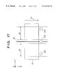
- FIG. 17 is an explanatory view of the fourth problem of the conventional surface position detection apparatus that uses electrostatic sensors
- FIG. 18 is an explanatory view of the fourth problem of the conventional surface position detection apparatus that uses electrostatic sensors
- FIG. 19 is an explanatory view of the criterion for selecting a sensor electrode of a tilt angle detection sensor formed from the sensor shown in FIG. 1;
- FIG. 20 is an explanatory view of a problem posed when a memory circuit is formed by exposure
- FIG. 21 is a flow chart showing a device manufacturing method using the exposure apparatus of the present invention.
- FIG. 22 is a flow chart showing details of the wafer process shown in FIG. 21 .
- FIG. 11 is a schematic view showing an exposure apparatus to which a surface position detection apparatus according to the first embodiment of the present invention can be applied.
- reference numeral 1 denotes a reticle
- 2 a reticle scanning stage (the scanning direction is the X direction)
- 3 an illumination system for exposing a wafer
- 4 a reduction projecting lens
- 5 a wafer
- 6 a wafer chuck
- 7 an X-Y stage
- 8 a Z ⁇ tilt stage
- 20 and 20 ′ electrostatic sensors constructing part of the surface position detection apparatus.
- the electrostatic sensors 20 and 20 ′ cannot measure the surface position of the wafer 5 at the exposure position.
- the sensor 20 is used, and when the wafer stage is to be scanned to the left (negative direction of the X axis), the sensor 20 ′ is used.
- a member 21 fixes the electrostatic sensors 20 and 20 ′ in position. To ground the electrostatic sensors through their housing, the member 21 is made of a metal material such as aluminum and grounded.
- Reference numeral 22 denotes a control circuit; 23 , a detection signal (to ten-odd kHz) from the electrostatic sensor; and 24 , a Z ⁇ tilt stage control signal.
- Each of the electrostatic sensors 20 and 20 ′ comprises at least two sensors lined up in the Y direction so as to detect yawing ( ⁇ x) in scanning the wafer stage in the X direction.
- the control circuit 22 calculates a surface position Z and tilt component (tilt) of the wafer 5 and controls the Z ⁇ tilt stage 8 , thereby accurately controlling the focus position.
- FIG. 12 is a view showing a conventional layout of electrostatic sensors when viewed from the direction of the optical axis.
- Reference numeral 25 denotes an exposure slit; and 27 , a scanning direction.
- three sensors 201 to 203 are used as an electrostatic sensor (corresponding to the electrostatic sensor 20 ) to detect the height and tilt of a wafer. Since the electrostatic sensors cannot directly measure the surface position at the exposure position, pre-measurement is performed by the sensors 201 to 203 mounted at positions separated from the exposure slit 25 by a predetermined distance in the scanning direction. Actually, since scanning is performed in the negative direction of the X axis, similar sensors must be mounted as an electrostatic sensor (corresponding to the electrostatic sensor 20 ′) in the negative direction, as described above with reference to FIG. 11, though they are not illustrated for descriptive convenience.
- FIG. 13 is a view showing the arrangement in FIG. 12 when viewed from one scanning direction (positive side of the Y axis).
- Reference numeral 26 denotes a surface (conductor) of an object (wafer) to be measured.
- the same reference numerals as in FIGS. 11 and 12 denote the same parts in FIG. 13 .
- the sensor 202 is used to detect the height of the wafer, and the sensors 201 and 203 are used to detect its tilt.
- S 1 , S 2 , and S 3 be the outputs from the sensors 201 to 203 , respectively.
- the height Z [ ⁇ m] and tilt ⁇ x [rad.] are given by
- FIG. 1 shows a variable distance measurement position electrostatic sensor used in the surface position detection apparatus of this embodiment, which is preferably stored in the exposure apparatus shown in FIG. 11 .
- Reference numerals 301 to 306 denote sensor electrodes. The section of each sensor electrode need not always be circular, as shown in FIG. 1.
- a change-over switch SW is used to arbitrarily select one of the sensor electrodes 301 to 306 . Unselected electrodes are preferably grounded or may electrically float.
- a conductive member 40 is called a guard ring and held at the same potential as that applied to the selected sensor electrode. The guard ring 40 prevents the current flowing through the sensor electrode from flowing beyond the electrode area, thereby allowing accurate measurement of the distance between the electrode and the object (not shown) to be measured.
- the same reference numerals as in FIG. 10 denote the same parts in FIG. 1 . With this arrangement, the distance between the object (not shown) to be measured and an electrode selected by the switch SW is measured at the position of the electrode.
- the distance measurement position can be changed by arbitrarily selecting one of the plurality of sensor electrodes by the change-over switch SW.
- the surface position detection apparatus of the present invention has a plurality of sensor electrodes that can be switched, and the number of sensor electrodes is not limited to six as in the above example. In this example, the sensor electrodes 301 to 306 are laid out in a line. However, the present invention is not limited to this layout, and any arbitrary layout can be employed. As will be described later, when this apparatus is used as the surface position detection apparatus of a semiconductor exposure apparatus, accurate focus control can be performed because the electrode positions are fixed, unlike an apparatus in which a plurality of electrostatic sensors are switched by a circuit. Switching is preferably electronic switching instead of mechanical switching. The switching timing and sensor electrode selection method will be described later in detail together with application examples.
- FIG. 2 is a view showing the principle of the variable distance measurement position electrostatic sensor shown in FIG. 1 .
- the change-over switch SW arbitrarily selects one of the plurality of sensor electrodes 301 to 306 arranged near an object 31 to be measured and connects the electrode to an electrical circuit.
- Reference symbols d 1 to d 6 denote distances between the sensor electrodes 301 to 306 and the conductive substrate 31 at the electrode positions, respectively. The distances may be different from each other depending on the surface shape of the conductive substrate 31 .
- the same reference numerals as in FIG. 10 or 1 denote the same parts in FIG. 2 .
- a high-frequency voltage is applied from an oscillator OS to, e.g., the electrode 305 selected by the change-over switch SW from the electrodes 301 to 306 .
- An ammeter AM is connected between the change-over switch SW and oscillator OS.
- the magnitude of the AC current flowing to the selected electrode 305 is measured by the ammeter AM and a measurement device 32 connected to the ammeter AM.
- the current measurement result is input to an arithmetic circuit 33 .
- the distance d 5 between the selected electrode 305 and the object 31 to be measured is measured by arithmetic processing by the arithmetic circuit 33 .
- FIG. 3 is a view for explaining an example in which the variable distance measurement position electrostatic sensor shown in FIGS. 1 and 2 is applied as the sensors 20 and 20 ′ for calculating the tilt angle of a wafer in the exposure apparatus shown in FIG. 11 .
- Variable distance measurement position electrostatic sensors 401 and 402 are used to calculate the tilt angle.
- Reference numerals 301 to 308 denote sensor electrodes.
- the sensor electrodes 301 to 304 construct the variable distance measurement position electrostatic sensor 401
- the sensor electrodes 305 to 308 construct the variable distance measurement position electrostatic sensor 402 .
- An exposure width 28 depends on the chip size formed on a wafer. Only a wafer portion positioned within this width is exposed.
- Reference symbol L′ denotes the distance between sensor electrodes used to calculate the tilt angle.
- a measurement circuit comprising the switch SW, ammeter AM, oscillator OS, and measurement device 32 is connected to each of the sensors 401 and 402 , as in FIGS. 1 and 2.
- the outputs from the two measurement devices 32 are supplied to the arithmetic circuit 33 .
- the switch SW, ammeter AM, oscillator OS, and measurement device 32 may be shared by the sensors 401 and 402 .
- the sensor electrode for detecting the tilt angle can be switched to an arbitrary sensor electrode by the switch SW to arbitrarily change the measurement position for tilt angle detection.
- the sensor 202 is used to detect the height to the surface of the object to be measured.
- FIG. 19 is an explanatory view of a sensor electrode selection method.
- the variable distance measurement position electrostatic sensors 401 and 402 are used to calculate the tilt angle of a wafer.
- the sensor electrode 301 constructs the variable distance measurement position electrostatic sensor 401
- the sensor electrodes 305 and 307 construct the variable distance measurement position electrostatic sensor 402 .
- Reference numeral 26 denotes the surface of a wafer (object to be measured). For illustrative convenience, the sensor for detecting the height and the remaining sensor electrodes are omitted.
- the same reference numerals as in FIG. 3 and the like denote the same parts in FIG. 19 .
- the influence of the minute structure on the surface can be made smaller in calculating the tilt angle, so the tilt angle can be accurately measured. That is, an outermost electrode within the exposure width is used as the sensor electrode for detecting the tilt angle.
- FIG. 14 is a view for explaining a problem posed when not the application example described with reference to FIG. 3 but the conventional electrostatic sensor shown in FIG. 10 is used for the surface position detection apparatus.
- the same reference numerals as in FIGS. 3 and 12 denote the same parts in FIG. 14 .
- the sensors 201 and 203 for detecting the tilt angle are positioned outside the exposure area.
- a wafer having a step difference on its surface because of the repeated process of forming layers has a large step difference between the interior and exterior of the exposure area.
- FIG. 4 is a view for explaining an application example shown in FIG. 3 that uses the variable distance measurement position electrostatic sensor of the present invention when viewed from the scanning direction.
- the same reference numerals as in FIG. 3 denote the same parts in FIG. 4 .
- accurate focus position control can be performed.
- FIG. 15 is a view for explaining another problem posed when not the application example described with reference to FIG. 4 but the conventional electrostatic sensor shown in FIG. 10 is used for the surface position detection apparatus when viewed from the scanning direction.
- the same reference numerals as in FIG. 12 or 14 denote the same parts in FIG. 15 .
- accurate focus position control cannot be performed.
- the electrostatic sensor according to the present invention when the electrostatic sensor according to the present invention is used to detect the tilt angle, the problem described with reference to FIG. 15 can be solved.
- FIG. 5 is a view for explaining in detail an example of measurement using the variable distance measurement position electrostatic sensor of the first embodiment shown in FIG. 1 as a sensor for detecting the tilt angle.
- the same reference numerals as in FIG. 3 denote the same parts in FIG. 5 .
- FIG. 16 is a view for explaining still another problem posed when not the application example described with reference to FIG. 4 but the conventional electrostatic sensor shown in FIG. 10 is used for the surface position detection apparatus.
- the same reference numerals as in FIG. 3 and the like denote the same parts in FIG. 16 .
- FIG. 16 when the exposure slit 25 is located near the outer peripheral portion of the wafer 5 , a sensor used in the surface position detection apparatus falls outside the range of the wafer, and the distance cannot be accurately measured. For this reason, even when the chip size can be ensured in the exposure area, the chip pattern cannot be printed by exposure, i.e., chips cannot be formed.
- FIG. 16 is a view for explaining still another problem posed when not the application example described with reference to FIG. 4 but the conventional electrostatic sensor shown in FIG. 10 is used for the surface position detection apparatus.
- the same reference numerals as in FIG. 3 and the like denote the same parts in FIG. 16 .
- use of the electrostatic sensor according to the present invention as a tilt angle detection sensor eliminates the conventional problem described with reference to FIG. 16 wherein when the exposure slit is positioned near the outer peripheral portion of the wafer, and some sensors fall outside the wafer range, the distance to the wafer cannot be measured, and exposure cannot be performed.
- the sensor electrode to be selected may change depending on the position of the exposure slit 25 .
- a sensor electrode within the area of the wafer must be selected.
- an electrode position determined in advance on the basis of the exposure width calculated immediately after chip layout data is input before the start of an exposure process is selected. That is, a sensor electrode that falls within the exposure width 28 and is located on the outermost side of the area of the wafer is selected.
- FIG. 6 is a view for explaining an example in which the variable distance measurement position electrostatic sensor of this embodiment is applied as a sensor for detecting the height in the surface position detection apparatus.
- a variable distance measurement position electrostatic sensor 403 is used to detect the height to the surface of the object to be measured.
- Reference numerals 311 and 312 denote sensor electrodes of the variable distance measurement position electrostatic sensor 403 .
- Reference numeral 29 denotes a scribing line (connection portion) between adjacent chips, which is positioned under the sensor electrode 311 .
- the same reference numerals as in FIG. 3 or 12 denote the same parts in FIG. 6 .
- the sensor electrode to be used in the height detection sensor 403 when the sensor electrode to be used in the height detection sensor 403 is switched to an arbitrary one of the sensor electrodes 311 and 312 using a switch (not shown), the sensor electrode (i.e., position of the sensor electrode to be used for detection) for detecting the height to the surface of the object to be measured can be arbitrarily changed.
- the sensors 201 and 203 are used to detect the tilt angle.
- the sensor electrode is switched to the sensor electrode 312 positioned within the exposure width 28 using the switch (not shown) to detect the height.
- Selection of the sensor electrode and actual processing of selecting the sensor electrode by using the switch are automatically done according to a program stored in the surface position detection apparatus. Since the user need not be aware of the algorithm or perform any operation, a cumbersome operation is unnecessary, and no errors occur. Switching is performed on the basis of the chip layout data before the start of an exposure process. The reason for this is as follows. Since the chip layout (pattern) is common to one wafer and does not change during exposure of the wafer, the sensor electrode used to detect the height does not change during the exposure process. The sensor electrode to be used to detect the height is determined on the basis of the exposure width determined from the data.
- FIG. 17 is a view for explaining still another problem posed when not the application example described with reference to FIG. 6 but the conventional electrostatic sensor shown in FIG. 10 is used for the surface position detection apparatus when viewed from the direction of the optical axis.
- FIG. 18 is a view for explaining this problem when viewed from the scanning direction.
- the same reference numerals as in FIG. 6 or 14 denote the same parts in FIGS. 17 and 18.
- the scribing line 29 is present within the exposure slit 25 . As shown in FIG. 18, even for a plurality of different chip patterns including this chip pattern, the scribing line 29 is positioned underneath the electrostatic sensor 202 for detecting the height Z.
- FIG. 7 is a view that best illustrates the characteristic feature of the detection area variable electrostatic sensor of a surface position detection apparatus according to the second embodiment of the present invention.
- a terminal 51 is connected to one of terminals 52 and 53 by a switch SW.
- Reference numeral 30 denotes a sensor electrode; and 30 ′, an electrode functioning as a sensor electrode only when the terminal 51 is connected to the terminal 52 by the switch SW.
- the electrode 30 ′ functions as a guard ring.
- the electrodes 30 and 30 ′ have sections concentric with each other.
- a high-frequency voltage is applied from an oscillator OS to only the electrode 30 or both the electrodes 30 and 30 ′ by the change-over switch SW.
- An ammeter AM is connected between the change-over switch SW and oscillator OS.
- the magnitude of the AC current flowing to only the electrode 30 or both the electrodes 30 and 30 ′ is measured by the ammeter AM and a measurement device 32 connected to the ammeter AM.
- the current measurement result is input to an arithmetic circuit 33 .
- the distance d 5 between the electrode 30 and a wafer as an object to be measured is measured by arithmetic processing by the arithmetic circuit 33 .
- the detection position can be changed.
- the detection area area of the sensor electrode
- the detection area can be changed. As described above, as one of the characteristic features of the electrostatic sensor, the detection area can be almost uniformly averaged. In the arrangement shown in FIG. 7, since the detection area can be changed, the area to be averaged can be changed.
- FIG. 8 is an explanatory view of the principle of the electrostatic sensor shown in FIG. 7, which allows to change the area of the sensor electrode, i.e., the detection area to be averaged.
- the same reference numerals as in FIG. 7 denote the same parts in FIG. 8 .
- the area (S 0 +S′) as the sum of an area S 0 of the sensor electrode 30 and an area S′ of the electrode 30 ′ can be set as the detection area.
- the terminal 51 to the terminal 53 not to make the electrode 30 ′ function as a sensor electrode only the area (S 0 ) of the sensor electrode 30 can be set as the detection area of the electrostatic sensor.
- the averaging area can be changed, and focus control can be easily performed in accordance with the layout of chips to be formed by exposure.
- FIG. 20 is a view for explaining that a conventional problem that defocus occurs depending on the chip layout can be solved by this embodiment, when viewed from the scanning direction.
- Reference numeral 41 denotes a surface of a memory cell; and 42 , a surface of a peripheral circuit.
- the same reference numerals as in FIG. 7 or 12 denote the same parts in FIG. 20 .
- Defocus may occur when the height position is adjusted along the surface of an object (resist) to be measured. This will be described with reference to FIG. 20.
- a device is roughly divided into the portion of the memory cell 41 and the portion of the peripheral circuit 42 . Exposure areas where critical resolving performance is required generally concentrate at the portion of the memory cell 41 .
- a relation S 2 ′ ⁇ Z′ ⁇ S 2 holds between a detected height position Z′, the height S 2 , and a height position S 2 ′ to the surface of the memory cell 41 .
- the specific value of Z′ is determined by the area of the memory cell 41 opposing the electrode 30 ′ and that of the peripheral circuit 42 .
- the height position Z′ i.e., the focus position can be made close to the height position S 2 ′.
- the surface of the memory cell 41 can be set within the focusing range, and the memory cell 41 and peripheral circuit 42 can be properly exposed.
- FIG. 21 shows the flow of manufacturing a microdevice (e.g., a semiconductor chip such as an IC or an LSI, a liquid crystal panel, a CCD, a thin-film magnetic head, or a micromachine).
- a microdevice e.g., a semiconductor chip such as an IC or an LSI, a liquid crystal panel, a CCD, a thin-film magnetic head, or a micromachine.
- step 1 circuit design
- step 2 mask preparation
- a mask having the designed pattern is prepared.
- step 3 wafer manufacture
- a wafer is manufactured using a material such as silicon or glass.
- step 4 wafer process
- an actual circuit is formed on the wafer by lithography using the prepared mask and wafer.
- step 5 a semiconductor chip is formed from the wafer prepared in step 4 .
- This step includes processes such as assembly (dicing and bonding) and packaging (chip encapsulation).
- step 6 inspections including an operation check test and a durability test of the semiconductor device manufactured in step 5 are performed.
- a semiconductor device is completed with these processes and delivered (step 7 ).
- FIG. 22 shows the detailed flow of the wafer process (step 4 ).
- step 11 oxidation
- step 12 CVD
- step 13 electrode formation
- step 14 ion implantation
- ions are implanted into the wafer.
- step 15 resist process
- step 16 exposure
- step 18 etching
- steps other than the developed resist image are etched.
- step 19 resist peeling
- the present invention even when the state of the surface to be detected changes, the position of the surface to be detected can be accurately detected in correspondence with the change. According to the exposure apparatus to which the present invention is applied, accurate focus control can be performed. Hence, accurate device manufacture is allowed.
- the position of the surface to be detected can be detected by selecting a sensor electrode in correspondence with the change. This allows efficient exposure and efficient device manufacture.
Landscapes
- Physics & Mathematics (AREA)
- General Physics & Mathematics (AREA)
- Exposure Of Semiconductors, Excluding Electron Or Ion Beam Exposure (AREA)
- Exposure And Positioning Against Photoresist Photosensitive Materials (AREA)
- Measurement Of Length, Angles, Or The Like Using Electric Or Magnetic Means (AREA)
Priority Applications (1)
| Application Number | Priority Date | Filing Date | Title |
|---|---|---|---|
| US10/059,294 US7072023B2 (en) | 1998-09-04 | 2002-01-31 | Position detection apparatus having a plurality of detection sections, and exposure apparatus |
Applications Claiming Priority (2)
| Application Number | Priority Date | Filing Date | Title |
|---|---|---|---|
| JP10-265797 | 1998-09-04 | ||
| JP26579798A JP4365908B2 (ja) | 1998-09-04 | 1998-09-04 | 面位置検出装置、露光装置およびデバイス製造方法 |
Related Child Applications (1)
| Application Number | Title | Priority Date | Filing Date |
|---|---|---|---|
| US10/059,294 Continuation US7072023B2 (en) | 1998-09-04 | 2002-01-31 | Position detection apparatus having a plurality of detection sections, and exposure apparatus |
Publications (2)
| Publication Number | Publication Date |
|---|---|
| US20020041367A1 US20020041367A1 (en) | 2002-04-11 |
| US6529263B2 true US6529263B2 (en) | 2003-03-04 |
Family
ID=17422181
Family Applications (2)
| Application Number | Title | Priority Date | Filing Date |
|---|---|---|---|
| US09/388,372 Expired - Fee Related US6529263B2 (en) | 1998-09-04 | 1999-09-01 | Position detection apparatus having a plurality of detection sections, and exposure apparatus |
| US10/059,294 Expired - Fee Related US7072023B2 (en) | 1998-09-04 | 2002-01-31 | Position detection apparatus having a plurality of detection sections, and exposure apparatus |
Family Applications After (1)
| Application Number | Title | Priority Date | Filing Date |
|---|---|---|---|
| US10/059,294 Expired - Fee Related US7072023B2 (en) | 1998-09-04 | 2002-01-31 | Position detection apparatus having a plurality of detection sections, and exposure apparatus |
Country Status (4)
| Country | Link |
|---|---|
| US (2) | US6529263B2 (de) |
| EP (1) | EP0984329A3 (de) |
| JP (1) | JP4365908B2 (de) |
| KR (1) | KR100354919B1 (de) |
Cited By (4)
| Publication number | Priority date | Publication date | Assignee | Title |
|---|---|---|---|---|
| US20040001192A1 (en) * | 2002-06-28 | 2004-01-01 | Lyons Joseph H. | System and method for automated focus measuring of a lithography tool |
| US20040178805A1 (en) * | 2003-03-13 | 2004-09-16 | Canon Kabushiki Kaisha | Capacitance sensor type measuring apparatus |
| CN104377142A (zh) * | 2013-08-14 | 2015-02-25 | 由田新技股份有限公司 | 物品检测方法及物品检测设备 |
| CN104377142B (zh) * | 2013-08-14 | 2016-11-30 | 由田新技股份有限公司 | 物品检测方法及物品检测设备 |
Families Citing this family (13)
| Publication number | Priority date | Publication date | Assignee | Title |
|---|---|---|---|---|
| TWI304158B (en) | 2003-01-15 | 2008-12-11 | Asml Netherlands Bv | Detection assembly and lithographic projection apparatus provided with such a detection assembly |
| JP4006364B2 (ja) * | 2003-06-19 | 2007-11-14 | キヤノン株式会社 | 計測装置 |
| US7332915B2 (en) * | 2004-09-28 | 2008-02-19 | General Electric Company | Sensor system and method of operating the same |
| KR100729263B1 (ko) * | 2005-07-14 | 2007-06-15 | 삼성전자주식회사 | 기판 노광 장치 |
| US7652489B2 (en) * | 2005-12-06 | 2010-01-26 | General Electric Company | Multi-range clearance measurement system and method of operation |
| US8013981B2 (en) | 2007-06-14 | 2011-09-06 | Asml Netherlands B.V. | Lithographic apparatus and device manufacturing method |
| US8237919B2 (en) * | 2007-08-24 | 2012-08-07 | Nikon Corporation | Movable body drive method and movable body drive system, pattern formation method and apparatus, exposure method and apparatus, and device manufacturing method for continuous position measurement of movable body before and after switching between sensor heads |
| WO2009028157A1 (ja) | 2007-08-24 | 2009-03-05 | Nikon Corporation | 移動体駆動方法及び移動体駆動システム、並びにパターン形成方法及びパターン形成装置 |
| NL2004054C2 (en) * | 2010-01-05 | 2011-07-06 | Mapper Lithography Ip Bv | Lithography system with capacitive sensing system. |
| WO2012123144A1 (en) * | 2011-03-11 | 2012-09-20 | Asml Netherlands B.V. | Electrostatic clamp apparatus and lithographic apparatus |
| NL2009612A (en) | 2011-11-21 | 2013-05-23 | Asml Netherlands Bv | Level sensor, a method for determining a height map of a substrate, and a lithographic apparatus. |
| KR101888940B1 (ko) * | 2012-03-28 | 2018-08-17 | 삼성전자주식회사 | 패턴 레이아웃을 디자인하는 방법 |
| WO2018144824A1 (en) * | 2017-02-02 | 2018-08-09 | TERA-print, LLC | Electrical contact auto-alignment strategy for highly parallel arrays in cantilever free scanning probe lithography |
Citations (31)
| Publication number | Priority date | Publication date | Assignee | Title |
|---|---|---|---|---|
| EP0004757A1 (de) | 1978-03-31 | 1979-10-17 | Gould Inc. | Kapazitives berührungsfreies Messystem |
| JPS57204547A (en) | 1981-06-12 | 1982-12-15 | Hitachi Ltd | Exposing method |
| JPS6165433A (ja) | 1984-09-07 | 1986-04-04 | Canon Inc | 対物レンズの物体位置検出装置 |
| JPH03253917A (ja) | 1990-03-05 | 1991-11-13 | Toshiba Corp | 間隔設定方法及び間隔設定装置 |
| US5091691A (en) * | 1988-03-21 | 1992-02-25 | Semitest, Inc. | Apparatus for making surface photovoltage measurements of a semiconductor |
| EP0572368A2 (de) | 1992-05-28 | 1993-12-01 | GOVERNMENT OF THE UNITED STATES OF AMERICA as represented by THE ADMINISTRATOR OF THE NATIONAL AERONAUTICS AND SPACE ADM. | Phasendiskriminierendes matrixförmiges kapazitives Sensorsystem |
| JPH07201698A (ja) | 1993-12-28 | 1995-08-04 | Hitachi Ltd | パターン露光用感光層形成方法及びこれを用いた半導体回路 |
| JPH07302748A (ja) | 1994-05-02 | 1995-11-14 | Canon Inc | 半導体露光装置 |
| US5593800A (en) * | 1994-01-06 | 1997-01-14 | Canon Kabushiki Kaisha | Mask manufacturing method and apparatus and device manufacturing method using a mask manufactured by the method or apparatus |
| JPH0945608A (ja) | 1995-08-03 | 1997-02-14 | Canon Inc | 面位置検出方法 |
| US5642056A (en) * | 1993-12-22 | 1997-06-24 | Tokyo Electron Limited | Probe apparatus for correcting the probe card posture before testing |
| EP0790479A1 (de) | 1996-02-14 | 1997-08-20 | STMicroelectronics S.r.l. | Kapazitiv Abstandssensor, insbesondere zur Erfassung von Fingerabdrücken |
| US5661408A (en) * | 1995-03-01 | 1997-08-26 | Qc Solutions, Inc. | Real-time in-line testing of semiconductor wafers |
| JPH09236425A (ja) | 1996-03-01 | 1997-09-09 | Canon Inc | 面位置検出方法 |
| JPH09246356A (ja) | 1996-03-01 | 1997-09-19 | Canon Inc | 表面位置設定方法 |
| GB2312514A (en) | 1996-02-13 | 1997-10-29 | Sensatech Ltd | Capacitive proximity or profile detector |
| JPH09293665A (ja) | 1996-04-26 | 1997-11-11 | Toshiba Corp | X線マスクの製造方法およびその製造装置 |
| JPH1064980A (ja) | 1996-08-22 | 1998-03-06 | Canon Inc | 面位置検出装置および方法 |
| JPH10141374A (ja) | 1996-11-06 | 1998-05-26 | Canon Inc | 能動静圧軸受装置および位置決めステージ |
| US5760879A (en) * | 1994-07-06 | 1998-06-02 | Canon Kabushiki Kaisha | Method of detecting coma of projection optical system |
| JPH10284393A (ja) | 1997-04-04 | 1998-10-23 | Canon Inc | 露光装置およびデバイス製造方法 |
| JPH10289871A (ja) | 1997-04-14 | 1998-10-27 | Nikon Corp | 投影露光装置 |
| JPH11111610A (ja) | 1997-10-01 | 1999-04-23 | Canon Inc | 位置決め方法及び位置決め装置 |
| JPH11121320A (ja) | 1997-10-09 | 1999-04-30 | Canon Inc | 面位置検出方法及び面位置検出装置 |
| US5917580A (en) * | 1996-08-29 | 1999-06-29 | Canon Kabushiki Kaisha | Scan exposure method and apparatus |
| JPH11176735A (ja) | 1997-12-09 | 1999-07-02 | Canon Inc | 面位置検出方法およびそれを用いた露光装置 |
| JPH11191522A (ja) | 1997-08-29 | 1999-07-13 | Canon Inc | 露光方法および装置 |
| US5988971A (en) | 1997-07-09 | 1999-11-23 | Ade Optical Systems Corporation | Wafer transfer robot |
| US6014203A (en) * | 1998-01-27 | 2000-01-11 | Toyo Technologies, Inc. | Digital electron lithography with field emission array (FEA) |
| US6341007B1 (en) | 1996-11-28 | 2002-01-22 | Nikon Corporation | Exposure apparatus and method |
| JP3253917B2 (ja) | 1997-03-29 | 2002-02-04 | シンポ株式会社 | 移動式無煙調理器における吸煙通路構造 |
Family Cites Families (3)
| Publication number | Priority date | Publication date | Assignee | Title |
|---|---|---|---|---|
| US5683547A (en) * | 1990-11-21 | 1997-11-04 | Hitachi, Ltd. | Processing method and apparatus using focused energy beam |
| US5651044A (en) * | 1995-10-02 | 1997-07-22 | General Electric Company | Capacitive proximity detector for radiation imager position control |
| EP0867771A3 (de) * | 1997-03-24 | 2000-10-25 | Nikon Corporation | Belichtungsapparat, Belichtungsverfahren und Verfahren zur Herstellung einer Schaltung |
-
1998
- 1998-09-04 JP JP26579798A patent/JP4365908B2/ja not_active Expired - Fee Related
-
1999
- 1999-09-01 US US09/388,372 patent/US6529263B2/en not_active Expired - Fee Related
- 1999-09-02 EP EP99306980A patent/EP0984329A3/de not_active Withdrawn
- 1999-09-04 KR KR1019990037599A patent/KR100354919B1/ko not_active Expired - Fee Related
-
2002
- 2002-01-31 US US10/059,294 patent/US7072023B2/en not_active Expired - Fee Related
Patent Citations (33)
| Publication number | Priority date | Publication date | Assignee | Title |
|---|---|---|---|---|
| EP0004757A1 (de) | 1978-03-31 | 1979-10-17 | Gould Inc. | Kapazitives berührungsfreies Messystem |
| JPS57204547A (en) | 1981-06-12 | 1982-12-15 | Hitachi Ltd | Exposing method |
| JPS6165433A (ja) | 1984-09-07 | 1986-04-04 | Canon Inc | 対物レンズの物体位置検出装置 |
| US5091691A (en) * | 1988-03-21 | 1992-02-25 | Semitest, Inc. | Apparatus for making surface photovoltage measurements of a semiconductor |
| JPH03253917A (ja) | 1990-03-05 | 1991-11-13 | Toshiba Corp | 間隔設定方法及び間隔設定装置 |
| EP0572368A2 (de) | 1992-05-28 | 1993-12-01 | GOVERNMENT OF THE UNITED STATES OF AMERICA as represented by THE ADMINISTRATOR OF THE NATIONAL AERONAUTICS AND SPACE ADM. | Phasendiskriminierendes matrixförmiges kapazitives Sensorsystem |
| US5642056A (en) * | 1993-12-22 | 1997-06-24 | Tokyo Electron Limited | Probe apparatus for correcting the probe card posture before testing |
| US5804983A (en) * | 1993-12-22 | 1998-09-08 | Tokyo Electron Limited | Probe apparatus with tilt correction mechanisms |
| JPH07201698A (ja) | 1993-12-28 | 1995-08-04 | Hitachi Ltd | パターン露光用感光層形成方法及びこれを用いた半導体回路 |
| US5593800A (en) * | 1994-01-06 | 1997-01-14 | Canon Kabushiki Kaisha | Mask manufacturing method and apparatus and device manufacturing method using a mask manufactured by the method or apparatus |
| US5658700A (en) | 1994-05-02 | 1997-08-19 | Canon Kabushiki Kaisha | Semiconductor manufacturing apparatus having a plurality of measurement devices and a semiconductor manufacturing method using the same |
| JPH07302748A (ja) | 1994-05-02 | 1995-11-14 | Canon Inc | 半導体露光装置 |
| US5760879A (en) * | 1994-07-06 | 1998-06-02 | Canon Kabushiki Kaisha | Method of detecting coma of projection optical system |
| US5661408A (en) * | 1995-03-01 | 1997-08-26 | Qc Solutions, Inc. | Real-time in-line testing of semiconductor wafers |
| JPH0945608A (ja) | 1995-08-03 | 1997-02-14 | Canon Inc | 面位置検出方法 |
| GB2312514A (en) | 1996-02-13 | 1997-10-29 | Sensatech Ltd | Capacitive proximity or profile detector |
| EP0790479A1 (de) | 1996-02-14 | 1997-08-20 | STMicroelectronics S.r.l. | Kapazitiv Abstandssensor, insbesondere zur Erfassung von Fingerabdrücken |
| JPH09246356A (ja) | 1996-03-01 | 1997-09-19 | Canon Inc | 表面位置設定方法 |
| JPH09236425A (ja) | 1996-03-01 | 1997-09-09 | Canon Inc | 面位置検出方法 |
| JPH09293665A (ja) | 1996-04-26 | 1997-11-11 | Toshiba Corp | X線マスクの製造方法およびその製造装置 |
| JPH1064980A (ja) | 1996-08-22 | 1998-03-06 | Canon Inc | 面位置検出装置および方法 |
| US5917580A (en) * | 1996-08-29 | 1999-06-29 | Canon Kabushiki Kaisha | Scan exposure method and apparatus |
| JPH10141374A (ja) | 1996-11-06 | 1998-05-26 | Canon Inc | 能動静圧軸受装置および位置決めステージ |
| US6341007B1 (en) | 1996-11-28 | 2002-01-22 | Nikon Corporation | Exposure apparatus and method |
| JP3253917B2 (ja) | 1997-03-29 | 2002-02-04 | シンポ株式会社 | 移動式無煙調理器における吸煙通路構造 |
| JPH10284393A (ja) | 1997-04-04 | 1998-10-23 | Canon Inc | 露光装置およびデバイス製造方法 |
| JPH10289871A (ja) | 1997-04-14 | 1998-10-27 | Nikon Corp | 投影露光装置 |
| US5988971A (en) | 1997-07-09 | 1999-11-23 | Ade Optical Systems Corporation | Wafer transfer robot |
| JPH11191522A (ja) | 1997-08-29 | 1999-07-13 | Canon Inc | 露光方法および装置 |
| JPH11111610A (ja) | 1997-10-01 | 1999-04-23 | Canon Inc | 位置決め方法及び位置決め装置 |
| JPH11121320A (ja) | 1997-10-09 | 1999-04-30 | Canon Inc | 面位置検出方法及び面位置検出装置 |
| JPH11176735A (ja) | 1997-12-09 | 1999-07-02 | Canon Inc | 面位置検出方法およびそれを用いた露光装置 |
| US6014203A (en) * | 1998-01-27 | 2000-01-11 | Toyo Technologies, Inc. | Digital electron lithography with field emission array (FEA) |
Cited By (10)
| Publication number | Priority date | Publication date | Assignee | Title |
|---|---|---|---|---|
| US20040001192A1 (en) * | 2002-06-28 | 2004-01-01 | Lyons Joseph H. | System and method for automated focus measuring of a lithography tool |
| US6885429B2 (en) * | 2002-06-28 | 2005-04-26 | Asml Holding N.V. | System and method for automated focus measuring of a lithography tool |
| US20050179883A1 (en) * | 2002-06-28 | 2005-08-18 | Asml Holding N.V. | System for automated focus measuring of a lithography tool |
| US7081948B2 (en) | 2002-06-28 | 2006-07-25 | Asml Holding N.V. | System for automated focus measuring of a lithography tool |
| US20040178805A1 (en) * | 2003-03-13 | 2004-09-16 | Canon Kabushiki Kaisha | Capacitance sensor type measuring apparatus |
| US7212015B2 (en) | 2003-03-13 | 2007-05-01 | Canon Kabushiki Kaisha | Capacitance sensor type measuring apparatus |
| US20070103171A1 (en) * | 2003-03-13 | 2007-05-10 | Canon Kabushiki Kaisha | Capacitance sensor type measuring apparatus |
| US7256590B2 (en) | 2003-03-13 | 2007-08-14 | Canon Kabushiki Kaisha | Capacitance sensor type measuring apparatus |
| CN104377142A (zh) * | 2013-08-14 | 2015-02-25 | 由田新技股份有限公司 | 物品检测方法及物品检测设备 |
| CN104377142B (zh) * | 2013-08-14 | 2016-11-30 | 由田新技股份有限公司 | 物品检测方法及物品检测设备 |
Also Published As
| Publication number | Publication date |
|---|---|
| US7072023B2 (en) | 2006-07-04 |
| EP0984329A3 (de) | 2002-05-02 |
| JP2000082658A (ja) | 2000-03-21 |
| US20020041367A1 (en) | 2002-04-11 |
| US20020093635A1 (en) | 2002-07-18 |
| KR100354919B1 (ko) | 2002-10-09 |
| EP0984329A2 (de) | 2000-03-08 |
| JP4365908B2 (ja) | 2009-11-18 |
| KR20000022922A (ko) | 2000-04-25 |
Similar Documents
| Publication | Publication Date | Title |
|---|---|---|
| US6529263B2 (en) | Position detection apparatus having a plurality of detection sections, and exposure apparatus | |
| EP1195647B1 (de) | Verfahren zur Detektion einer Oberflächenlage und Abtastbelichtungsverfahren unter Verwendung derselbe | |
| JP2756620B2 (ja) | 半導体露光方法およびその装置 | |
| US6668075B1 (en) | Position detection apparatus and method | |
| JP3254916B2 (ja) | 投影光学系のコマ収差を検出する方法 | |
| US6583430B1 (en) | Electron beam exposure method and apparatus | |
| JP3210145B2 (ja) | 走査型露光装置及び該装置を用いてデバイスを製造する方法 | |
| JP3315540B2 (ja) | 位置計測装置、位置合わせ装置、露光装置およびデバイスの製造方法 | |
| JP2009200122A (ja) | 露光装置およびデバイス製造方法 | |
| KR19980081185A (ko) | 포토리소그래피용 다중 검출기 정렬 시스템 | |
| JP4392914B2 (ja) | 面位置検出装置、露光装置、およびデバイス製造方法 | |
| US6426508B1 (en) | Surface-position detection device, a projection exposure apparatus using the device, and a device manufacturing method using the apparatus | |
| JP3814384B2 (ja) | 面位置検出方法及び面位置検出装置 | |
| TW518704B (en) | Shape measuring method, shape measuring device, exposing method, exposing device, and device manufacturing method | |
| JP2000012455A (ja) | 荷電粒子線転写露光装置及び荷電粒子線転写露光装置におけるマスクと感応基板の位置合わせ方法 | |
| JPH11195579A (ja) | 露光装置及び露光方法 | |
| JP3441930B2 (ja) | 走査型露光装置およびデバイス製造方法 | |
| JPH104055A (ja) | 自動焦点合わせ装置及びそれを用いたデバイスの製造方法 | |
| JP2006030021A (ja) | 位置検出装置及び位置検出方法 | |
| JP3198718B2 (ja) | 投影露光装置及びそれを用いた半導体素子の製造方法 | |
| JPH11121325A (ja) | 投影露光装置 | |
| JP3397654B2 (ja) | ディストーション変化量の計測方法及びそれを利用した投影露光装置並びにそれらを用いたデバイスの製造方法 | |
| JPH11251232A (ja) | 基板および露光装置および素子製造方法 | |
| JP2006024681A (ja) | 位置計測装置及び方法並びに露光装置及び方法 | |
| JP2002139847A (ja) | 露光装置、露光方法及びデバイス製造方法 |
Legal Events
| Date | Code | Title | Description |
|---|---|---|---|
| AS | Assignment |
Owner name: CANON KABUSHIKI KAISHA, JAPAN Free format text: ASSIGNMENT OF ASSIGNORS INTEREST;ASSIGNORS:OGURI, HISAAKI;SASAKI, TOYOSHIGE;HASEGAWA, MASANOBU;REEL/FRAME:010408/0971;SIGNING DATES FROM 19991007 TO 19991012 |
|
| FEPP | Fee payment procedure |
Free format text: PAYOR NUMBER ASSIGNED (ORIGINAL EVENT CODE: ASPN); ENTITY STATUS OF PATENT OWNER: LARGE ENTITY |
|
| FPAY | Fee payment |
Year of fee payment: 4 |
|
| REMI | Maintenance fee reminder mailed | ||
| LAPS | Lapse for failure to pay maintenance fees | ||
| STCH | Information on status: patent discontinuation |
Free format text: PATENT EXPIRED DUE TO NONPAYMENT OF MAINTENANCE FEES UNDER 37 CFR 1.362 |
|
| FP | Lapsed due to failure to pay maintenance fee |
Effective date: 20110304 |