US6556459B2 - Uninterruptible power supply and method of turning off AC switch for uninterruptible power supply - Google Patents
Uninterruptible power supply and method of turning off AC switch for uninterruptible power supply Download PDFInfo
- Publication number
- US6556459B2 US6556459B2 US10/180,692 US18069202A US6556459B2 US 6556459 B2 US6556459 B2 US 6556459B2 US 18069202 A US18069202 A US 18069202A US 6556459 B2 US6556459 B2 US 6556459B2
- Authority
- US
- United States
- Prior art keywords
- sinusoidal voltage
- voltage vref
- power supply
- synchronous
- power
- Prior art date
- Legal status (The legal status is an assumption and is not a legal conclusion. Google has not performed a legal analysis and makes no representation as to the accuracy of the status listed.)
- Expired - Lifetime
Links
Images




Classifications
-
- H—ELECTRICITY
- H02—GENERATION; CONVERSION OR DISTRIBUTION OF ELECTRIC POWER
- H02J—ELECTRIC POWER NETWORKS; CIRCUIT ARRANGEMENTS OR SYSTEMS FOR SUPPLYING OR DISTRIBUTING ELECTRIC POWER; SYSTEMS FOR STORING ELECTRIC ENERGY
- H02J9/00—Circuit arrangements for emergency or stand-by power supply, e.g. for emergency lighting
- H02J9/04—Circuit arrangements for emergency or stand-by power supply, e.g. for emergency lighting in which the distribution system is disconnected from the normal source and connected to a standby source
- H02J9/06—Circuit arrangements for emergency or stand-by power supply, e.g. for emergency lighting in which the distribution system is disconnected from the normal source and connected to a standby source with automatic change-over, e.g. UPS systems
- H02J9/062—Circuit arrangements for emergency or stand-by power supply, e.g. for emergency lighting in which the distribution system is disconnected from the normal source and connected to a standby source with automatic change-over, e.g. UPS systems for AC powered loads
Definitions
- the present invention relates to an uninterruptible power supply which connects a load to utility power supply through an AC switch.
- AC switches used in conventional uninterruptible power supplies employ switching element with a self turn-off function or thyristors that are turned off by a forced turn-off circuit.
- AC switch Another type of AC switch is also used which does not use a turn-off circuit and is naturally turned off as a current flowing in the thyristor falls below a holding current.
- the use of the AC switch incorporating only such thyristors can reduce the cost of the uninterruptible power supply.
- a period occurs without fail during which two AC powers are parallelly connected to and fed to a load, delaying the turn-off of the AC switch, as indicated in Japanese Patent Laid-Open Nos. 5-30683, 5-176461 and 5-292686.
- a conventional thyristor-based AC switch 1 for each phase has antiparallelly connected thyristors SCR 1 and SCR 2 disposed between a utility or commercial power supply 3 and a power converter 5 for each phase.
- the power converter 5 has a function of converting an AC power into a DC power and vice versa, and is connected to a DC power supply 7 on a DC side thereof.
- the electric power from the utility power supply 3 is fed through the AC switch 1 to a load 9 , and the output from the power converter 5 is supplied directly to the load 9 .
- An object of the present invention is to provide an uninterruptible power supply capable of turning off an AC switch made up of thyristors as quickly as possible.
- Another object of the present invention is to provide an uninterruptible power supply capable of turning off an AC switch made up of thyristors as quickly as possible by using a power converter.
- Still another object of the present invention is to provide an uninterruptible power supply capable of turning off an AC switch made up of thyristors without providing a separate, forced turn-off circuit.
- Yet another object of the present invention is to provide an AC switch turn-off method for an uninterruptible power supply capable of turning off an AC switch made up of thyristors without providing a separate, forced turn-off circuit.
- the present invention improves an uninterruptible power supply which comprises: a first feeding path to feed an AC power to a load from a utility power supply through an AC switch made up of a pair of antiparallelly connected thyristors; a second feeding path including a voltage control type power converter, the power converter using a DC power supply as its source and performing an inverter operation of converting a DC power into an AC power and feeding the converted AC power to the load; a reference sinusoidal voltage generation circuit to produce a reference sinusoidal voltage; a control command generation means to, based on the reference sinusoidal voltage, output to the power converter a voltage control command to cause the power converter to perform the inverter operation, wherein, while the voltage control command is being output from the control command generation means, the AC switch is turned off and the feeding of the AC power to the load is switched over from the first feeding path to the second feeding path.
- the AC switch is arranged for each phase. Thus, for a three-phase AC power, three single-phase AC switches are provided, one for each phase.
- the reference sinusoidal voltage generation circuit includes: a sinusoidal voltage generation means to generate a synchronous sinusoidal voltage Vref 1 , a high synchronous sinusoidal voltage Vref 2 and a low synchronous sinusoidal voltage Vref 3 , wherein the synchronous sinusoidal voltage Vref 1 is synchronized with the utility power supply and, when used as the reference sinusoidal voltage, causes an output voltage of the power converter to become almost equal to a voltage of the utility power supply, the high synchronous sinusoidal voltage Vref 2 is in phase with the synchronous sinusoidal voltage Vref 1 and higher in amplitude than the synchronous sinusoidal voltage Vref 1 , and the low synchronous sinusoidal voltage Vref 3 is in phase with the synchronous sinusoidal voltage Vref 1 and lower in amplitude than the synchronous sinusoidal voltage Vref 1 ; a current detection means to detect a current flowing through the AC switch; and a sinusoidal voltage selection means to select the synchronous sinusoidal voltage Vref 1 , the high synchronous sinusoidal voltage Vref 2 and a low
- the reference sinusoidal voltage generation circuit includes: a sinusoidal voltage generation means to generate a synchronous sinusoidal voltage Vref 1 , a high synchronous sinusoidal voltage Vref 2 and a low synchronous sinusoidal voltage Vref 3 , wherein the synchronous sinusoidal voltage Vref 1 is synchronized with the utility power supply and, when used as the reference sinusoidal voltage, causes an output voltage of the power converter to become almost equal to a voltage of the utility power supply, the high synchronous sinusoidal voltage Vref 2 is in phase with the synchronous sinusoidal voltage Vref 1 and higher in amplitude than the synchronous sinusoidal voltage Vref 1 , and the low synchronous sinusoidal voltage Vref 3 is in phase with the synchronous sinusoidal voltage Vref 1 and lower in amplitude than the synchronous sinusoidal voltage Vref 1 ; a current detection means to detect a current flowing through the AC switch; and a sinusoidal voltage selection means to select the synchronous sinusoidal voltage Vref 1 , the high synchronous sinusoidal voltage Vref 2 and a low
- the reference sinusoidal voltage generation circuit when the first feeding path is switched over to the second switching path, the reference sinusoidal voltage generation circuit generates a reference sinusoidal voltage that causes the output voltage of the power converter in the second feeding path to apply a reverse bias to the conducting one of the thyristors making up the AC switch in the first feeding path.
- the AC switch can be turned off quickly without providing a forced turn-off circuit for the thyristors.
- no period exists during which the utility power supply and the power converter are connected in parallel thus ensuring that no cross current flows between the utility power supply and the power converter.
- the present invention can also be applied to a normally utility power type uninterruptible power supply which normally supplies electric power to the load through the first feeding path and, in the event a failure of the utility power supply, switches the power feeding from the first feeding path to the second feeding path.
- the control command generation means outputs a voltage control command while the utility power failure persists.
- the present invention can also be applied to a normally utility power feeding and active filter type uninterruptible power supply which normally supplies power to the load through the first feeding path and operates the power converter as an active filter and, in the event a failure of the utility power supply, switches the power feeding from the first feeding path to the second feeding path.
- the control command generation means is made to output a voltage control command to the power converter while the power failure persists in the utility power supply and, when there is no power failure in the utility power supply, output to the power converter a current control command that causes it to operate as an active filter.
- the present invention can also be applied to a normally inverter type uninterruptible power supply which normally supplies electric power to the load through the second feeding path and, when the power converter is abnormal, switches the feeding from the second feeding path to the first feeding path.
- the control command generation means is made to output a voltage control command at all times when the power converter is normal.
- the AC switch is turned on.
- the control command generation means when the power converter is restored or repaired from the abnormal condition and the first feeding path is switched over to the second feeding path, the control command generation means generates a voltage control command.
- the present invention also improves an uninterruptible power supply which comprises: a power failure detection means to detect a power failure in a utility power supply; an AC switch having a pair of antiparallelly connected thyristors, the AC switch being adapted to conduct to feed an AC power from the utility power supply to a load when the utility power supply is normal and, when the utility power supply fails, turn off; a DC power supply; a voltage control type power converter arranged between the AC switch and the DC power supply, wherein when the utility power supply is normal, the power converter performs a rectifier operation of converting the AC power from the utility power supply into a DC power and charging the DC power supply with the DC power and an active filter operation of compensating for a harmonic current and a reactive current flowing into the load and wherein at other times the power converter uses the DC power supply as its source and performs mainly an inverter operation of converting a DC power into an AC power and feeding the converted AC power to the load; a reference sinusoidal voltage generation circuit to produce a reference sinusoidal voltage;
- the sinusoidal voltage generation means may have, but is not limited to, a configuration in which it generates the synchronous sinusoidal voltage Vref 1 , a high synchronous sinusoidal voltage Vref 2 in phase with and a voltage difference command value ⁇ V higher than the synchronous sinusoidal voltage Vref 1 , and a low synchronous sinusoidal voltage Vref 3 in phase with and a voltage difference command value ⁇ V lower than the synchronous sinusoidal voltage Vref 1 .
- This arrangement can easily produce sinusoidal voltages required for various controls. In particular, this arrangement can reliably determine the necessary reverse bias voltage by the voltage difference command value ⁇ V, so it is possible to output from the power converter a minimum voltage required to turn off the thyristor at whatever timing the AC switch is to be turned off.
- the sinusoidal voltage selection means may also be constructed to have a first selection circuit to select the high synchronous sinusoidal voltage Vref 2 when the output of the current detection means has a positive polarity and the low synchronous sinusoidal voltage Vref 3 when the output of the current detection means has a negative polarity; a first decision circuit to decide that the output voltage of the first selection circuit is required as the reference sinusoidal voltage when the power failure detection means detects a power failure and the current detection means detects that the current is not zero; and a second selection circuit to select the output voltage of the first selection circuit when the first decision circuit decides that the output voltage of the first selection circuit is required and, at other times, select the synchronous sinusoidal voltage Vref 1 .
- the necessary sinusoidal voltage can reliably be selected with a few selection circuits.
- three kinds of sinusoidal voltages Vref 1 -Vref 3 are the same in phase with each other are used to generate a reference sinusoidal voltage that causes the power converter to produce a reverse bias voltage to be applied to the thyristors making up the AC switch. It is also possible to use three kinds of sinusoidal voltages different in phase from one another to generate a reverse bias voltage.
- the uninterruptible power supply comprises: a power failure detection means to detect a power failure in a utility power supply; an AC switch having a pair of antiparallelly connected thyristors, the AC switch being adapted to conduct to feed an AC power from the utility power supply to a load when the utility power supply is normal and, when the utility power supply fails, turn off; a DC power supply; a voltage control type power converter arranged between the AC switch and the DC power supply, wherein when the utility power supply is normal, the power converter performs a rectifier operation of converting the AC power from the utility power supply into a DC power and charging the DC power supply with the DC power and an active filter operation of compensating for a harmonic current and a reactive current flowing into the load and wherein at other times the power converter uses the DC power supply as its source and performs mainly an inverter operation of converting a DC power into an AC power and feeding the converted AC power to the load; a phase shift type reference sinusoidal voltage generation circuit to produce a reference sinusoidal voltage; and
- the AC switch comprises a pair of antiparallelly connected thyristors.
- This invention uses the phase shift type reference sinusoidal voltage generation circuit to generate three kinds of sinusoidal voltages different in phase from one another.
- the phase shift type reference sinusoidal voltage generation circuit comprises: a phase shift type sinusoidal voltage generation means to generate a synchronous sinusoidal voltage Vref 1 , a leading sinusoidal voltage Vref 4 and a lagging sinusoidal voltage Vref 5 , wherein the synchronous sinusoidal voltage Vref 1 is synchronized with the utility power supply and, when used as the reference sinusoidal voltage, causes an output voltage of the power converter to become almost equal in amplitude to a voltage of the utility power supply, the leading sinusoidal voltage Vref 4 is equal in amplitude to and leading in phase the synchronous sinusoidal voltage Vref 1 , and the lagging sinusoidal voltage Vref 5 is equal in amplitude to and lagging in phase the synchronous sinusoidal voltage Vref 1 ; a current detection means to detect a current flowing through
- the thyristors forming the AC switch can be turned off in a short time.
- this period is very short and, once this period is passed, either of the leading sinusoidal voltage Vref 4 or the lagging sinusoidal voltage Vref 5 becomes larger in absolute value than the synchronous sinusoidal voltage Vref 1 without fail.
- the AC switch can be turned off with only a small time delay. Therefore no practical problem arises with this invention.
- the phase shift type sinusoidal voltage generation means may be configured to produce the synchronous sinusoidal voltage Vref 1 , the leading sinusoidal voltage Vref 4 equal in amplitude to and leading in phase the synchronous sinusoidal voltage Vref 1 by a phase difference command value ⁇ , and the lagging sinusoidal voltage Vref 5 equal in amplitude to and lagging in phase the synchronous sinusoidal voltage Vref 1 by the phase difference command value ⁇ .
- the phase shift type sinusoidal voltage selection means selects the leading sinusoidal voltage Vref 4 , the lagging sinusoidal voltage Vref 5 or the synchronous sinusoidal voltage Vref 1 and outputs the selected voltage as the reference sinusoidal voltage to the control command generation means, wherein the phase shift type sinusoidal voltage selection means selects the leading sinusoidal voltage Vref 4 after the current has changed from the negative polarity to the positive polarity until the synchronous sinusoidal voltage Vref 1 reaches a positive peak value, selects the lagging sinusoidal voltage Vref 5 after the synchronous sinusoidal voltage has reached the positive peak value until the current changes from the positive polarity to the negative polarity, selects the leading sinusoidal voltage Vref 4 after the current has changed from the positive polarity to the negative polarity until the synchronous sinusoidal voltage reaches a negative peak value, selects the lagging sinusoidal voltage Vref 5 after the synchronous sinusoidal voltage has reached the negative peak value until the current changes from the negative polarity to the positive polarity, and selects the
- the present invention also relates to an AC switch turn-off method for an uninterruptible power supply, wherein the uninterruptible power supply has a first feeding path to feed an AC power to a load from a utility power supply through an AC switch made up of a pair of antiparallelly connected thyristors and a second feeding path including a voltage control type power converter, the power converter using a DC power supply as its source and performing an inverter operation of converting a DC power into an AC power and feeding the converted AC power to the load.
- a reverse bias voltage from the power converter is applied to a conducting one of the thyristors to forcibly turn off the conducting thyristor.
- FIG. 1 is a control block diagram of a first embodiment of the present invention
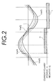
- FIG. 2 is an operation waveform diagram of the first embodiment of the present invention.
- FIG. 3 is a detailed diagram of a first selection circuit used in the first embodiment
- FIG. 4 is a diagram showing changes over time of current and voltage in this invention when a power failure is detected
- FIG. 5 is a control block diagram of a second embodiment of the present invention.
- FIG. 6 is an operation waveform diagram of the second embodiment of the present invention.
- FIGS. 7A and 7B are detailed logic diagrams of a first selection circuit of the second embodiment.
- FIGS. 8A, 8 B, and 8 C are diagrams showing configurations of uninterruptible power supplies to which the present invention can be applied.
- FIG. 1 is a circuit block diagram schematically showing one example configuration in which the present invention is applied to an uninterruptible power supply of normally utility power and active filter type.
- FIG. 1 shows only a single phase component, i.e., connections and a control system for one phase.
- an AC switch 1 a voltage control type power converter 5 and a DC power supply 7 are basically the same as the conventional ones.
- the voltage control type power converter 5 is installed between the AC switch 1 and the DC power supply 7 .
- the power converter 5 When the utility power is normal, the power converter 5 performs a rectifier operation in which it converts an AC power from a three-phase AC utility power supply 3 into a DC power and charges the DC power supply 7 with the rectified DC power and also an active filter operation that generates currents to compensate for a harmonic current and a reactive current flowing into the load 9 . At other times, the power converter 5 performs mainly an inverter operation in which it converts a DC power from the DC power supply 7 into an AC power and supplies the inverted AC power to the load 9 . As shown in FIG. 8A, the load 9 is supplied from the utility power supply 3 through the first feeding path R 1 during the rectifier operation and, during the inverter operation, from the power converter 5 through the second feeding path R 2 .
- the AC switch 1 installed between the utility power supply 3 and the power converter 5 corresponds to one phase and comprises two antiparallelly connected thyristors SCR 1 and SCR 2 .
- the load 9 is supplied with an AC power from the utility power supply 3 through the AC switch 1 .
- the AC switch 1 is opened to stop supplying the AC power from the utility power supply 3 to the load 9 .
- a reference sinusoidal voltage generation circuit 11 When a power failure detection means 12 detects the presence or absence of a power failure, a reference sinusoidal voltage generation circuit 11 outputs a reference sine wave signal for controlling the power converter 5 to a control command generation means 13 . Based on the reference sinusoidal voltage, the control command generation means 13 outputs to the power converter 5 a voltage control command for having the power converter 5 perform the inverter operation and a current control command for having the power converter 5 perform the rectifier operation and the active filter operation.
- the power failure detection means 12 may, for example, have a known configuration which determines the occurrence of a power failure when a voltage detection circuit detects that a voltage of one phase is lower than a predetermined voltage.
- the control command generation means 13 actually receives signals representing information necessary for the control of the voltage and current on the AC side of the power converter 5 and the DC voltage on the DC side.
- the configurations of the power converter 5 and the control command generation means 13 are disclosed in Japanese Patent Laid-Open Nos. 8-51735, 9-56087 and 10-14251 and also detailed in Japanese Patent Application 2000-288480 (U.S. Ser. No. 09/956,185, EP Application No. 01250328.0), a previous application by this applicant.
- the reference sinusoidal voltage generation circuit 11 comprises a current detection means 11 a for detecting a current flowing through the AC switch 1 , a sinusoidal voltage generation means 11 b for generating a sine wave voltage to be output as the reference sinusoidal voltage to the control command generation means 13 , and a sinusoidal voltage selection means 11 c for selecting a sine wave voltage to be output as the reference sinusoidal voltage to the control command generation means 13 .
- the current detection means 11 a based on an analog current value detected by a current transformer CT, outputs a current detection signal necessary for the control.
- the sinusoidal voltage generation means 11 b generates a synchronous sinusoidal voltage Vref 1 , a high synchronous sinusoidal voltage Vref 2 , and a low synchronous sinusoidal voltage Vref 3 .
- the synchronous sinusoidal voltage Vref 1 is synchronized with the utility power supply 3 and, when used as the reference sinusoidal voltage, causes the output voltage of the power converter 5 to be almost equal to the voltage of the utility power supply 3 .
- the high synchronous sinusoidal voltage Vref 2 is in phase with the synchronous sinusoidal voltage Vref 1 and larger in amplitude than the synchronous sinusoidal voltage Vref 1 .
- the low synchronous sinusoidal voltage Vref 3 is in phase with the synchronous sinusoidal voltage Vref 1 and smaller in amplitude than the synchronous sinusoidal voltage Vref 1 .
- the output voltage of the power converter 5 appears on a line 17 b of FIG. 1 .
- the synchronous sinusoidal voltage Vref 1 is used as the reference sinusoidal voltage Vref, an AC output equal in phase and amplitude to the AC voltage of the utility power supply 3 is produced on the line 17 b .
- the sinusoidal voltage selection means lie selects the synchronous sinusoidal voltage Vref 1 when the power failure detection means 12 does not detect a power outage or a power failure.
- the sinusoidal voltage selection means 11 c selects the high synchronous sinusoidal voltage Vref 2 when the output of the current detection means 11 a has a positive polarity, the low synchronous sinusoidal voltage Vref 3 when the output of the current detection means 11 a has a negative polarity, and the synchronous sinusoidal voltage Vref 1 when the output of the current detection means 11 a is zero, before outputting the selected sinusoidal voltage as the reference sinusoidal voltage to the control command generation means 13 .
- the reference sinusoidal voltage generation circuit 11 selects the high synchronous sinusoidal voltage Vref 2 or low synchronous sinusoidal voltage Vref 3 .
- the conducting thyristor SCR 1 or SCR 2 of the AC switch 1 is applied a reverse bias and turned off.
- the AC switch 1 remains turned off and the power converter 5 starts the inverter operation.
- the power failure detection means 12 does not detect the power outage, the reference sinusoidal voltage generation circuit 11 outputs the synchronous sinusoidal voltage Vref 1 .
- the control command generation means 13 uses the synchronous sinusoidal voltage Vref 1 as its input, the control command generation means 13 performs an active filter operation. This operation is detailed in the previous application and thus its explanation is omitted here.
- the sinusoidal voltage generation means 11 b in this example generates the high synchronous sinusoidal voltage Vref 2 by adding a voltage difference command value ⁇ V to the synchronous sinusoidal voltage Vref 1 synchronized with the utility power supply 3 , and the low synchronous sinusoidal voltage Vref 3 by subtracting the voltage difference command value ⁇ V from the synchronous sinusoidal voltage Vref 1 .
- the voltage difference command value ⁇ V is preset based on thyristor characteristics to produce a reverse bias voltage that can reliably effect a turn-off.
- FIG. 2 shows waveforms of the synchronous sinusoidal voltage Vref 1 , the high synchronous sinusoidal voltage Vref 2 and the low synchronous sinusoidal voltage Vref 3 and a waveform of an AC current I. Since the load is inductive, the waveform of the AC current I lags the synchronous sinusoidal voltage Vref 1 .
- the sinusoidal voltage output from the reference sinusoidal voltage generation circuit 11 can be expressed as follows.
- Vref Vref 1 + ⁇ V ⁇ sign( I ) ⁇ S (1)
- symbol I is assumed to be a current value as detected by the current detection means 11 a .
- the reference sinusoidal voltage Vref is the synchronous sinusoidal voltage Vref 1 , making the voltage of the line 17 b almost equal to the voltage of the utility power supply 3 .
- the conducting thyristor of the AC switch 1 remains turned on.
- equation (2) or (3) holds for the reference sinusoidal voltage Vref of equation (1).
- the reference sinusoidal voltage Vref switches from the synchronous sinusoidal voltage Vref 1 to the synchronous sinusoidal voltage indicated by a thick line in the graph of FIG. 2 .
- the reference sinusoidal voltage Vref in equation (1) returns to the synchronous sinusoidal voltage Vref 1 .
- the current detection means 11 a detects a positive current, the current is flowing through the antiparallelly connected thyristor SCR 1 , as shown in FIG. 4 A.
- the line 17 b is applied a voltage Vrb, which is ⁇ V higher than the voltage V of the utility power supply 3 , and the thyristor SCR 1 is impressed with a reverse bias of ⁇ V, causing the current I to drop to zero.
- FIG. 4B shows how the voltage and current waveforms change over time in this situation. As shown in FIG.
- the sinusoidal voltage selection means 11 c selects the low synchronous sinusoidal voltage Vref 3 as the reference sinusoidal voltage and a reverse bias is applied to the thyristor SCR 2 , thus interrupting the current flowing through the thyristor SCR 2 .
- the sinusoidal voltage generation means 11 b in the reference sinusoidal voltage generation circuit 11 shown in FIG. 1 produces the synchronous sinusoidal voltage Vref 1 , the high synchronous sinusoidal voltage Vref 2 and the low synchronous sinusoidal voltage Vref 3 by using the voltage difference command value ⁇ V.
- the sinusoidal voltage generation means 11 b may use a PLL circuit for instance.
- a first selection circuit 11 c 1 in the sinusoidal voltage selection means 11 c selects the high synchronous sinusoidal voltage Vref 2 when the output of the current detection means 11 a is positive and the low synchronous sinusoidal voltage Vref 3 when the output of the current detection means 11 a is negative.
- FIG. 3 shows a detailed configuration of the first selection circuit 11 c 1 .
- a first decision circuit 11 c 2 decides that an output voltage of the first selection circuit 11 c 1 is required as the reference sinusoidal voltage.
- the second selection circuit 11 c 3 selects the output voltage of the first selection circuit 11 c 1 .
- the second selection circuit 11 c 3 selects the synchronous sinusoidal voltage Vref 1 .
- FIG. 5 is a block diagram showing another embodiment (phase difference method) of the present invention. Parts identical with those of FIG. 1 are assigned like reference numerals.
- a phase shift type reference sinusoidal voltage generation circuit 19 is used as the reference sinusoidal voltage generation circuit.
- the phase shift type reference sinusoidal voltage generation circuit 19 comprises a current detection means 19 a for detecting a current flowing through the AC switch 1 , a phase shift type sinusoidal voltage generation means 19 b , and a phase shift type sinusoidal voltage selection means 19 c .
- the phase shift type sinusoidal voltage generation means 19 b generates the synchronous sinusoidal voltage Vref 1 used in the first embodiment, a leading sinusoidal voltage Vref 4 which is equal in amplitude to and leading in phase the synchronous sinusoidal voltage Vref 1 , and a lagging sinusoidal voltage Vref 5 which is equal in amplitude to and lagging in phase the synchronous sinusoidal voltage Vref 1 .
- the phase shift type sinusoidal voltage selection means 19 c selects the synchronous sinusoidal voltage Vref 1 when the power failure detection means 12 does not detect a power outage.
- the phase shift type sinusoidal voltage selection means 19 c selects the leading sinusoidal voltage Vref 4 or the lagging sinusoidal voltage Vref 5 whichever is larger in amplitude than the synchronous sinusoidal voltage while the current I is positive. While the current I is negative, the phase shift type sinusoidal voltage selection means 19 c selects whichever of the leading and lagging sinusoidal voltages Vref 4 and Vref 5 is smaller in amplitude than the synchronous sinusoidal voltage. When the output of the current detection means is zero, the phase shift type sinusodial voltage selection means 19 c selects the synchronous sinusoidal voltage Vref 1 . The selected sinusoidal voltage is then output as the reference sinusoidal voltage to the control command generation means 13 .
- the phase shift type sinusoidal voltage generation means 19 b generates a cosine wave voltage V cos which leads the synchronous sinusoidal voltage Vref 1 by 90 degrees. This cosine wave voltage is used by the phase shift type sinusoidal voltage selection means 19 c described later.
- the operation of the uninterruptible power supply shown in FIG. 5 will be explained with reference to waveforms of FIG.
- FIG. 6 illustrates waveforms of the synchronous sinusoidal voltage Vref 1 , the leading sinusoidal voltage Vref 4 and the lagging sinusoidal voltage Vref 5 and also a waveform of the current I.
- the phase shift type reference sinusoidal voltage generation circuit 19 outputs the leading sinusoidal voltage Vref 4 as the reference sinusoidal voltage.
- the phase shift type reference sinusoidal voltage generation circuit 19 outputs the lagging sinusoidal voltage Vref 5 as the reference sinusoidal voltage to the load line 17 b .
- a transition of the reference sinusoidal voltage that depends on the product of the current and the cosine wave voltage V cos is shown by a thick line.
- Comparison in amplitude between the thick line voltage and the synchronous sinusoidal voltage Vref 1 synchronized with the utility power supply 3 shows that the voltage applied to the AC switch 1 is reverse-biased with respect to the current. This arrangement causes a reverse bias to be applied to the current-carrying thyristor thus interrupting the current in that thyristor.
- the synchronous sinusoidal voltage Vref 1 matches the voltage on the line 17 b in amplitude and phase.
- ⁇ represents a phase shift angle.
- the synchronous sinusoidal voltage Vref 1 lies between the leading sinusoidal voltage Vref 4 and the lagging sinusoidal voltage Vref 5 in most area.
- Vref 4 or Vref 5 is larger than the synchronous sinusoidal voltage Vref 1 and whichever is smaller Vref 4 or Vref 5 , is smaller than the synchronous sinusoidal voltage Vref 1 . Therefore, in an area where
- Vref 4 when I>0, then Vref 4 >Vref 5 , Vref 4 is selected as the voltage of the line 17 b .
- Vref 4 when I ⁇ 0, then Vref 4 ⁇ Vref 5 , thus the lagging sinusoidal voltage Vref 5 is chosen as the voltage of the line 17 b so that the current-carrying thyristor is applied a reverse bias.
- the left-hand member of equation (8) can be rewritten as
- the absolute value of sin ⁇ is larger than the absolute value of sin ( ⁇ ). That is, the synchronous sinusoidal voltage Vref 1 is larger than the leading sinusoidal voltage Vref 4 and the lagging sinusoidal voltage Vref 5 . Thus, during this period the current-carrying thyristor cannot be applied a reverse bias voltage and turned off. Therefore, the period of the phase shift angle ⁇ during the phase angle ⁇ is the percentage of the time that the thyristor cannot be turned off.
- the phase shift angle ⁇ is sufficiently small compared with ⁇ , the time during which the thyristor cannot be turned off can be kept sufficiently short. Therefore, the effect of the delayed thyristor turn-off can be kept to the minimum.
- the phase shift type sinusoidal voltage selection means 19 c outputs the synchronous sinusoidal voltage Vref 1 .
- phase shift type reference sinusoidal voltage generation circuit 19 The configuration of the phase shift type reference sinusoidal voltage generation circuit 19 that realizes the above-described functions will be explained by referring to FIG. 5 .
- the phase shift type sinusoidal voltage generation means 19 b generates and outputs the synchronous sinusoidal voltage Vref 1 , the leading sinusoidal voltage Vref 4 , the lagging sinusoidal voltage Vref 5 and the cosine wave voltage V cos. More specifically, the phase shift type sinusoidal voltage generation means 19 b may be realized with a PLL circuit.
- a first selection circuit 19 c 1 that forms a part of the phase shift type sinusoidal voltage selection means 19 c selects the leading sinusoidal voltage Vref 4 when the product of the current output from the current detection means 19 a and the cosine wave voltage V cos is positive and the lagging sinusoidal voltage Vref 5 when the product of the current output from current detection means and V cos is negative.
- a first decision circuit 19 c 2 decides that the output voltage of the first selection circuit 19 c 1 is required for the reference sinusoidal voltage.
- a second selection circuit 19 c 3 selects the output voltage of the first selection circuit 19 c 1 .
- the second selection circuit 19 c 3 selects the synchronous sinusoidal voltage Vref 1 .
- FIG. 7A shows an example logic circuit of the first selection circuit 19 c 1 of FIG. 5 .
- Input signals to the first selection circuit 19 c 1 of FIG. 5 are V cos, Vref 4 and Vref 5 .
- Generated from these signals are input signals BV and BV cos to the logic circuit of FIG. 7A, and a same polarity signal X.
- These input signals BV, BV cos go High when the synchronous sinusoidal voltage Vref 1 and the cosine wave voltage V cos are positive, respectively.
- the input signals BV and BV cos are also pulsed logic signals that go Low when the synchronous sinusoidal voltage Vref 1 and the cosine wave voltage V cos are negative, respectively.
- the same polarity signal X goes High when the signs of the synchronous sinusoidal voltage Vref 1 and the current I flowing through the thyristor are the same and goes Low when they are opposite.
- the logic diagram of FIG. 7A can be expressed by the following logic equation.
- FIG. 7B shows another example of a logic circuit of the first selection circuit 19 c 1 of FIG. 5 .
- the first selection circuit 19 c 1 receives pulsed logic signals BV cos and BI at its inputs which go High when the cosine wave voltage V cos and the current I flowing through the thyristor are positive, respectively, and which go Low when they are negative.
- the block diagram of FIG. 5 does not show these logical input signals, they can be derived from the input signals I and V cos shown in the figure.
- the logic diagram of FIG. 7B may be expressed by the following logic equation.
- equation (15) when I>0 and V cos>0, the first term goes High; and when I ⁇ 0 and V cos ⁇ 0, the second term goes High. Hence, in equation (15) Y becomes High when I ⁇ V cos >0. This matches the condition of the first decision circuit described earlier.
- the output of the decision circuit of FIG. 7B is High, the leading sinusoidal voltage Vref 4 is selected; and when the output is Low, the lagging sinusoidal voltage Vref 5 is selected.
- FIG. 8B shows a configuration of an uninterruptible power supply to which the present invention can be applied.
- the utility power supply 3 normally feeds the load 9 through the first feeding path R 1 . If the utility power supply 3 should fail, a DC power from a storage battery 21 is converted by the power converter 5 into an AC power before being fed to the load 9 through the second feeding path R 2 . At this time the power converter 5 operates as an inverter. In this uninterruptible power supply, too, during a power failure the first feeding path R 1 is switched over to the second feeding path R 2 , so that the AC switch 1 must be turned off quickly.
- FIG. 8C shows a configuration of another uninterruptible power supply to which the present invention can be applied.
- an AC power from the utility power supply 3 is converted by a power converter 23 into a DC power which is used to charge a storage battery 21 and the DC output of the power converter 23 is converted by the power converter 5 into an AC power which is then fed to the load 9 during a normal condition.
- This equipment is called a normally inverter feeding method. With this equipment, in the event of a failure of the second feeding path R 2 , the AC switch turns on feeding the load through the first feeding path R 1 . When, after the recovery of the second feeding path R 2 , the first feeding path R 1 is switched over to the second feeding path R 2 , the AC switch 1 is turned off.
- the configuration of this invention for turning off the AC switch 1 used in the first and second embodiment shown in FIG. 1 through FIG. 7 can be adopted to turn off the AC switch 1 instantaneously.
- the reference sinusoidal voltage generation circuit in the event that the utility power supply falls, since the reference sinusoidal voltage generation circuit generates a reference sinusoidal voltage that sets an output voltage of the power converter to such a level as can apply a reverse bias to a conducting one of the thyristors making up the AC switch, the AC switch can be turned off quickly without having to provide a special, forced thyristor turn-off circuit.
- the invention as defined in claim 1 offers an advantage that during the process of turning off the AC switch, there exists no period of time when the utility power supply and the power converter are paralleled, thus preventing a cross current from flowing between the utility power supply and the power converter.
Landscapes
- Business, Economics & Management (AREA)
- Emergency Management (AREA)
- Engineering & Computer Science (AREA)
- Power Engineering (AREA)
- Stand-By Power Supply Arrangements (AREA)
Applications Claiming Priority (2)
| Application Number | Priority Date | Filing Date | Title |
|---|---|---|---|
| JP2001193357 | 2001-06-26 | ||
| JP2001-193357 | 2001-06-26 |
Publications (2)
| Publication Number | Publication Date |
|---|---|
| US20020195879A1 US20020195879A1 (en) | 2002-12-26 |
| US6556459B2 true US6556459B2 (en) | 2003-04-29 |
Family
ID=19031662
Family Applications (1)
| Application Number | Title | Priority Date | Filing Date |
|---|---|---|---|
| US10/180,692 Expired - Lifetime US6556459B2 (en) | 2001-06-26 | 2002-06-26 | Uninterruptible power supply and method of turning off AC switch for uninterruptible power supply |
Country Status (3)
| Country | Link |
|---|---|
| US (1) | US6556459B2 (de) |
| EP (1) | EP1276202B1 (de) |
| DE (1) | DE60224477T2 (de) |
Cited By (12)
| Publication number | Priority date | Publication date | Assignee | Title |
|---|---|---|---|---|
| US20040196005A1 (en) * | 2003-04-04 | 2004-10-07 | Sanyo Denki Co., Ltd. | Uninterruptible power supply device with circuit for degradation judgment of storage battery |
| US20040223347A1 (en) * | 2003-03-31 | 2004-11-11 | Fuji Electric Holdings Co., Ltd. | Uninterruptible power supply system |
| US20120069616A1 (en) * | 2010-09-17 | 2012-03-22 | Toshiba Lighting & Technology Corporation | Switching power supply device, and adjustable power supply system including the same |
| US20130163294A1 (en) * | 2011-12-27 | 2013-06-27 | Korea Electronics Technology Institute | Inverter apparatus having power supply circuit |
| US20130194847A1 (en) * | 2012-01-31 | 2013-08-01 | The Prosser Group Llc Dba Green Charge Networks | Universal power conversion methods and systems |
| US8791597B2 (en) | 2010-03-12 | 2014-07-29 | Liebert Corporation | Uninterruptible power supply with a dual gain voltage regulator controlling an inverter output voltage based on active and reactive components of current |
| US8823338B2 (en) | 2012-01-31 | 2014-09-02 | Green Charge Networks Llc | Universal single-stage power converter |
| US9160202B2 (en) | 2012-01-31 | 2015-10-13 | General Electric Company | Control system for uninterruptible power supplies |
| US9236768B2 (en) | 2012-01-31 | 2016-01-12 | Lorenzo Giuntini | Systems, methods, and devices for control of parallel uninterruptible power supplies |
| CN108370174A (zh) * | 2015-12-01 | 2018-08-03 | 东芝三菱电机产业系统株式会社 | 不间断电源装置 |
| US10042007B2 (en) | 2015-02-04 | 2018-08-07 | Liebert Corporation | Method for detecting a failing rectifier or rectifier source |
| US11201537B2 (en) * | 2019-05-22 | 2021-12-14 | Sungrow Power Supply Co., Ltd. | Method for suppressing common mode impulse current for inverter generated when switching on alternating current switch and application device thereof |
Families Citing this family (11)
| Publication number | Priority date | Publication date | Assignee | Title |
|---|---|---|---|---|
| US7786616B2 (en) * | 2003-02-07 | 2010-08-31 | Cummins Power Generation Inc. | Generator with DC boost and split bus bidirectional DC-to-DC converter for uninterruptible power supply system or for enhanced load pickup |
| GR1007463B (el) * | 2009-10-23 | 2011-11-18 | Αλεξανδρος Γεωργιου Κατσουλης | Μεθοδος και συσκευη αναγνωρισης διακοπης ρευματος σε διακοπτομενο ηλεκτρολογικο σημειο εναλλασσομενου δικτυου |
| US8310104B2 (en) * | 2010-03-14 | 2012-11-13 | Gengenbach Gary A | Substantially bumpless transfer grid synchronization |
| EP2720338B1 (de) * | 2012-10-10 | 2021-06-09 | FIMER S.p.A. | Verfahren und Vorrichtung zum Erkennen des Inselbetriebs eines verteilten Stromgenerators |
| KR101590698B1 (ko) * | 2014-03-31 | 2016-02-01 | 엘지전자 주식회사 | 전원 판단 장치 |
| US10284007B2 (en) | 2014-10-23 | 2019-05-07 | Abb Schweiz Ag | Protection methods and switches in uninterruptible power supply systems |
| EP3291411B1 (de) | 2016-09-01 | 2019-05-08 | Maschinenfabrik Reinhausen GmbH | Verfahren zum steuern einer unterbrechungsfreien stromversorgung und anlage für eine unterbrechungsfreie stromversorgung |
| CN110999061B (zh) * | 2017-07-27 | 2023-06-20 | 东芝三菱电机产业系统株式会社 | 交流开关及具备该交流开关的不间断电源装置和电压暂降补偿装置 |
| US10148124B1 (en) * | 2018-01-05 | 2018-12-04 | Channel Well Technology Co., Ltd. | Uninterrupted power bank capable of supplying high DC voltage during interruption of main supply and providing AC voltage as normal supply of the main supply |
| CN113285691B (zh) * | 2020-02-19 | 2024-03-08 | 瑞昱半导体股份有限公司 | 滤波器、滤波方法以及滤波系统 |
| TWI795978B (zh) * | 2021-11-03 | 2023-03-11 | 台達電子工業股份有限公司 | 具有路徑強迫關斷功能之不斷電裝置及其路徑強迫關斷方法 |
Citations (6)
| Publication number | Priority date | Publication date | Assignee | Title |
|---|---|---|---|---|
| US5111374A (en) * | 1990-06-22 | 1992-05-05 | The University Of Tennessee Research Corp. | High frequency quasi-resonant DC voltage notching scheme of a PWM voltage fed inverter for AC motor drives |
| US5111376A (en) * | 1990-11-01 | 1992-05-05 | Sundstrand Corporation | Voltage balancing circuit |
| JPH0530683A (ja) | 1991-07-23 | 1993-02-05 | Fuji Electric Co Ltd | 無停電電源装置の電源切替え方法 |
| JPH05176461A (ja) | 1991-12-20 | 1993-07-13 | Yuasa Corp | 交流電源装置 |
| JPH05292686A (ja) | 1992-04-10 | 1993-11-05 | Toyo Electric Mfg Co Ltd | 交流スイッチ装置 |
| US6160722A (en) * | 1999-08-13 | 2000-12-12 | Powerware Corporation | Uninterruptible power supplies with dual-sourcing capability and methods of operation thereof |
Family Cites Families (6)
| Publication number | Priority date | Publication date | Assignee | Title |
|---|---|---|---|---|
| DE2904786C2 (de) * | 1979-02-08 | 1981-02-19 | Siemens Ag, 1000 Berlin Und 8000 Muenchen | Verfahren zur Regelung von Wechselrichtern im Parallelbetrieb und Schaltungsanordnungen zur Durchführung des Verfahrens |
| JPS58112423A (ja) * | 1981-12-26 | 1983-07-04 | 株式会社東芝 | 電力変換設備の制御方式 |
| JPS60249832A (ja) * | 1984-05-25 | 1985-12-10 | 株式会社東芝 | インバ−タの保護方法 |
| JP2695941B2 (ja) * | 1989-09-22 | 1998-01-14 | 株式会社東芝 | 無停電電源装置 |
| DE69011312T2 (de) * | 1990-01-29 | 1994-12-01 | Toshiba Kawasaki Kk | Wechselrichtersteuerungsgerät. |
| ATE274764T1 (de) * | 2000-06-01 | 2004-09-15 | Liebert Corp | Vorrichtung und verfahren für eine schnelle fehlererkennung und übertragung in eine geräteinteraktive unterbrechungsfreie stromversorgung |
-
2002
- 2002-06-25 DE DE60224477T patent/DE60224477T2/de not_active Expired - Lifetime
- 2002-06-25 EP EP02254419A patent/EP1276202B1/de not_active Expired - Lifetime
- 2002-06-26 US US10/180,692 patent/US6556459B2/en not_active Expired - Lifetime
Patent Citations (6)
| Publication number | Priority date | Publication date | Assignee | Title |
|---|---|---|---|---|
| US5111374A (en) * | 1990-06-22 | 1992-05-05 | The University Of Tennessee Research Corp. | High frequency quasi-resonant DC voltage notching scheme of a PWM voltage fed inverter for AC motor drives |
| US5111376A (en) * | 1990-11-01 | 1992-05-05 | Sundstrand Corporation | Voltage balancing circuit |
| JPH0530683A (ja) | 1991-07-23 | 1993-02-05 | Fuji Electric Co Ltd | 無停電電源装置の電源切替え方法 |
| JPH05176461A (ja) | 1991-12-20 | 1993-07-13 | Yuasa Corp | 交流電源装置 |
| JPH05292686A (ja) | 1992-04-10 | 1993-11-05 | Toyo Electric Mfg Co Ltd | 交流スイッチ装置 |
| US6160722A (en) * | 1999-08-13 | 2000-12-12 | Powerware Corporation | Uninterruptible power supplies with dual-sourcing capability and methods of operation thereof |
Cited By (22)
| Publication number | Priority date | Publication date | Assignee | Title |
|---|---|---|---|---|
| US20040223347A1 (en) * | 2003-03-31 | 2004-11-11 | Fuji Electric Holdings Co., Ltd. | Uninterruptible power supply system |
| US7019989B2 (en) * | 2003-03-31 | 2006-03-28 | Fuji Electric Holdings Co., Ltd. | Uninterruptible power supply system |
| US20040196005A1 (en) * | 2003-04-04 | 2004-10-07 | Sanyo Denki Co., Ltd. | Uninterruptible power supply device with circuit for degradation judgment of storage battery |
| US7612468B2 (en) * | 2003-04-04 | 2009-11-03 | Sanyo Denki Co., Ltd. | Uninterruptible power supply device with circuit for degradation judgment of storage battery |
| US20100013316A1 (en) * | 2003-04-04 | 2010-01-21 | Sanyo Denki Co., Ltd. | Uninterruptible power supply device with circuit for degradation judgment of storage battery |
| US7759822B2 (en) * | 2003-04-04 | 2010-07-20 | Sanyo Denki Co., Ltd. | Uninterruptible power supply device with circuit for degradation judgment of storage battery |
| US8791597B2 (en) | 2010-03-12 | 2014-07-29 | Liebert Corporation | Uninterruptible power supply with a dual gain voltage regulator controlling an inverter output voltage based on active and reactive components of current |
| US8797015B2 (en) * | 2010-09-17 | 2014-08-05 | Toshiba Lighting & Technology Corporation | Switching power supply device, and adjustable power supply system including the same |
| CN102412709B (zh) * | 2010-09-17 | 2015-05-13 | 东芝照明技术株式会社 | 开关电源装置以及可调节电源系统 |
| CN102412709A (zh) * | 2010-09-17 | 2012-04-11 | 东芝照明技术株式会社 | 开关电源装置以及可调节电源系统 |
| US20120069616A1 (en) * | 2010-09-17 | 2012-03-22 | Toshiba Lighting & Technology Corporation | Switching power supply device, and adjustable power supply system including the same |
| US8891263B2 (en) * | 2011-12-27 | 2014-11-18 | Korea Electronics Technology Institute | Inverter apparatus having power supply circuit |
| US20130163294A1 (en) * | 2011-12-27 | 2013-06-27 | Korea Electronics Technology Institute | Inverter apparatus having power supply circuit |
| US8823338B2 (en) | 2012-01-31 | 2014-09-02 | Green Charge Networks Llc | Universal single-stage power converter |
| US20130194847A1 (en) * | 2012-01-31 | 2013-08-01 | The Prosser Group Llc Dba Green Charge Networks | Universal power conversion methods and systems |
| US8897041B2 (en) * | 2012-01-31 | 2014-11-25 | Green Charge Networks Llc | Universal power conversion methods and systems |
| US9160202B2 (en) | 2012-01-31 | 2015-10-13 | General Electric Company | Control system for uninterruptible power supplies |
| US9236768B2 (en) | 2012-01-31 | 2016-01-12 | Lorenzo Giuntini | Systems, methods, and devices for control of parallel uninterruptible power supplies |
| US10042007B2 (en) | 2015-02-04 | 2018-08-07 | Liebert Corporation | Method for detecting a failing rectifier or rectifier source |
| CN108370174A (zh) * | 2015-12-01 | 2018-08-03 | 东芝三菱电机产业系统株式会社 | 不间断电源装置 |
| CN108370174B (zh) * | 2015-12-01 | 2021-06-04 | 东芝三菱电机产业系统株式会社 | 不间断电源装置 |
| US11201537B2 (en) * | 2019-05-22 | 2021-12-14 | Sungrow Power Supply Co., Ltd. | Method for suppressing common mode impulse current for inverter generated when switching on alternating current switch and application device thereof |
Also Published As
| Publication number | Publication date |
|---|---|
| DE60224477D1 (de) | 2008-02-21 |
| EP1276202A2 (de) | 2003-01-15 |
| US20020195879A1 (en) | 2002-12-26 |
| EP1276202A3 (de) | 2005-01-05 |
| EP1276202B1 (de) | 2008-01-09 |
| DE60224477T2 (de) | 2009-02-26 |
Similar Documents
| Publication | Publication Date | Title |
|---|---|---|
| US20020195879A1 (en) | Uninterruptible power supply and method of turning off AC switch for uninterruptible power supply | |
| US4876433A (en) | Inverter controlled-type power source for arc welding | |
| US6144191A (en) | Voltage regulator | |
| WO2015198447A1 (ja) | 無停電電源装置 | |
| EP2827487B1 (de) | Stromrichter | |
| US11394295B2 (en) | Power supply apparatus | |
| JPWO2019021416A1 (ja) | 交流スイッチならびにそれを備える無停電電源装置および瞬低補償装置 | |
| EP1450476B1 (de) | Stromrichterschaltung | |
| US6545481B1 (en) | Power interruption detection | |
| JP3771200B2 (ja) | 無停電電源装置及び無停電電源装置の交流スイッチ遮断方法 | |
| JP3469918B2 (ja) | 無停電電源装置 | |
| JPH09247952A (ja) | 無停電運転方法及び電源装置 | |
| JPH08205423A (ja) | 無停電電源装置 | |
| JP2018198478A (ja) | 電源装置 | |
| JP3550573B2 (ja) | 電力変換装置 | |
| JP4374605B2 (ja) | Pwmサイクロコンバータ | |
| JP2002320331A (ja) | 系統連系電力変換システムの制御装置 | |
| JP2009254102A (ja) | 無停電電源装置 | |
| JP3826722B2 (ja) | 無停電工事用電源装置 | |
| JP4893113B2 (ja) | 整流回路の制御装置 | |
| JPS59117470A (ja) | 電力制御回路 | |
| JPH01278266A (ja) | 交流電源装置 | |
| JPH0488847A (ja) | 交流無停電電源装置 | |
| JP2005168197A (ja) | 交流交流直接変換装置の制御装置 | |
| KR102797634B1 (ko) | 위상 동기 제어 회로 및 그것을 이용한 전력 변환 장치 |
Legal Events
| Date | Code | Title | Description |
|---|---|---|---|
| AS | Assignment |
Owner name: SANYO DENKI CO., LTD., JAPAN Free format text: ASSIGNMENT OF ASSIGNORS INTEREST;ASSIGNORS:OKUI, YOSHIAKI;YANAGISAWA, MINORU;REEL/FRAME:013137/0393 Effective date: 20020606 |
|
| STCF | Information on status: patent grant |
Free format text: PATENTED CASE |
|
| CC | Certificate of correction | ||
| FPAY | Fee payment |
Year of fee payment: 4 |
|
| FEPP | Fee payment procedure |
Free format text: PAYER NUMBER DE-ASSIGNED (ORIGINAL EVENT CODE: RMPN); ENTITY STATUS OF PATENT OWNER: LARGE ENTITY Free format text: PAYOR NUMBER ASSIGNED (ORIGINAL EVENT CODE: ASPN); ENTITY STATUS OF PATENT OWNER: LARGE ENTITY |
|
| FPAY | Fee payment |
Year of fee payment: 8 |
|
| FPAY | Fee payment |
Year of fee payment: 12 |