US6590401B1 - Capacitive proximity switch for evaluating minor changes in capacitance and method therefor - Google Patents
Capacitive proximity switch for evaluating minor changes in capacitance and method therefor Download PDFInfo
- Publication number
- US6590401B1 US6590401B1 US09/762,356 US76235601A US6590401B1 US 6590401 B1 US6590401 B1 US 6590401B1 US 76235601 A US76235601 A US 76235601A US 6590401 B1 US6590401 B1 US 6590401B1
- Authority
- US
- United States
- Prior art keywords
- bridge
- voltage
- face
- capacitor
- diagonal
- Prior art date
- Legal status (The legal status is an assumption and is not a legal conclusion. Google has not performed a legal analysis and makes no representation as to the accuracy of the status listed.)
- Expired - Fee Related
Links
Images




Classifications
-
- G—PHYSICS
- G01—MEASURING; TESTING
- G01V—GEOPHYSICS; GRAVITATIONAL MEASUREMENTS; DETECTING MASSES OR OBJECTS; TAGS
- G01V3/00—Electric or magnetic prospecting or detecting; Measuring magnetic field characteristics of the earth, e.g. declination, deviation
- G01V3/08—Electric or magnetic prospecting or detecting; Measuring magnetic field characteristics of the earth, e.g. declination, deviation operating with magnetic or electric fields produced or modified by objects or geological structures or by detecting devices
- G01V3/088—Electric or magnetic prospecting or detecting; Measuring magnetic field characteristics of the earth, e.g. declination, deviation operating with magnetic or electric fields produced or modified by objects or geological structures or by detecting devices operating with electric fields
-
- H—ELECTRICITY
- H03—ELECTRONIC CIRCUITRY
- H03K—PULSE TECHNIQUE
- H03K17/00—Electronic switching or gating, i.e. not by contact-making and –breaking
- H03K17/94—Electronic switching or gating, i.e. not by contact-making and –breaking characterised by the way in which the control signals are generated
- H03K17/945—Proximity switches
- H03K17/955—Proximity switches using a capacitive detector
Definitions
- the invention relates to a capacitive proximity switch for the evaluation of capacitance changes with an electrical alternating current measurement bridge of four bridge branches, which reach every two of four switching knots of the bridge, wherein an alternating current is positioned as a bridge feed voltage near two opposite, not neighboring switching knots, and respectively the two bridge branches between the two feed in switching knots build each of the two halves of the bridge, and there is an evaluated bridge diagonal voltage on the two remaining switching knots over diagonal voltage path, wherein the bridge diagonal voltage is removable, for detecting an approaching or moving away face, in particular an electrically bad conductive face or metallic face, which face is part of variable capacitor in one of the bridge branches of the bridge circuit, wherein at least one capacitor (capacitive bridge) or at least one capacitor and/or one resistor (capacitive ohmic bridge) is disposed in the remaining bridge branches as further reactences, wherein rectifiers are arranged to the rectification of the both bridge branch voltages separately according to respective bridge halves in the diagonal voltage paths and the diagonal bridge voltage is evaluated only after
- integrated circuits are furthermore known for the determination of small changes in capacitance.
- the integrated circuits exhibit the disadvantage that in most cases a ground free capacitance is necessary.
- such circuits require in general a digital evaluation unit (mostly a counter) which means a large expenditure for switching technology.
- Such concepts are employed predominantly in the micro systems technology for these reasons.
- the amplitude of the alternating voltage is very small based on the small change in capacitance, namely a few millivolts mV;
- the frequency of the alternating voltage, which is employed for operating the bridge, and therewith also the frequency of the bridge diagonal voltage is located in the MHz region in order to avoid that the branch currents do not assume too small values given the small capacity values;
- the bridge diagonal voltage in many cases in addition to the alternating voltage component also includes a common mode direct current component with a substantial larger as compared to the alternating current component.
- a circuit arrangement for eliminating the influence of a phase shift between the voltage potentials of the two measurement points of an alternating current measurement bridge with complex resistances is furnished, wherein the difference of the voltage potentials forms the measurement signal.
- a rectifier valve is disposed between the measurement points and the input enclosures of a circuit for forming the difference in each voltage path, wherein a storage disposed between the output of the rectifier valve and a reference potential common to the alternating current measurement bridge is connected following to each of the rectifier valves.
- Capacitors employed as capacitive measurement value receivers within an alternating current measurement bridge, either in a bridge circuit with four capacitances or with two capacitances and two resistors, wherein in each case a capacitance is variable, are known from the literature location Heinz Schneider, Kondensatoren als Messwertauf Spotify (Capacitors as measurement value receivers), Elektronik-Ap rates Nr. 14, Jul. 9, 1985.
- a proximity switch with an alternating current measurement bridge is known by FR-A-2371676, which is subjected to an alternating current.
- the bridge branch voltages are rectified and subject to single electrical manipulations. Only after the rectification of the bridge branch voltages these as changing direct current as capacitive size are evaluated.
- the proximity switch comprises a flat multilayer circuit board comprising at least two electrically insulating layers, wherein an electrically conductingly intermediate player is disposed between the two electrically insulating layers as a first place of capacitance in one of the two bridge branches of one of the bridge halves and wherein a flat electrically conducting covering is placed on one of the two layers furnishing a sensor, wherein the flat covering forms the second face of the capacitor, wherein the face is disposed movable relative to the sensor and forms with the sensor a second flat variable capacitor, and wherein the face and the sensor form one capacitance and wherein the sensor and the electrically conducting intermediate layer form the second capacitance of one of the two bridge halves and wherein this construction represents the one half of the bridge, and wherein rectifires are disposed in the diagonal voltage paths for rectifying the two bridge branch voltages separately according to the respective bridge half and wherein the bridge diagonal voltage is evaluated only after the rectification of the two bridge branch voltages as the direct current changing corresponding to the capacitance change of the variable
- the proximity switch and the method are associated with the advantage that a reliable evaluation of very small capacitance changes is possible, wherein the circuit exhibits a high stability against interferences and a high-temperature stability and wherein the circuit is substantially insensitive relative to coupled in interferences. Similarly the proximity switch can be realized with comparatively small expenditures.
- the advantages comprise in particular:
- a slow operational amplifier or, respectively, comparator can be employed for evaluating the bridge diagonal voltage.
- the rectification of the bridge branch voltages can be performed with diodes, whereby the very simple circuit with only a few device elements results; advantageously a so-called slow diode can be employed in order to suppress interferences.
- rectification is performed synchronous with controlled switches, in case a particularly high suppression of interferences is required.
- the rectifiers of the two branches exhibit the same temperature behavior in order for the rectified bridge diagonal voltage to be independent of temperature. It is advantageous for good suppression of interferences that the switching construction is furnished symmetrical, because an interference operating in the same way onto the two bridge branches does not cause the difference voltage at the rectifier outputs.
- the rectification of the bridge branch voltages can be performed either by diodes, preferably four diodes, or by controlled switches, preferably four controlled switches, wherein in case of the employment of switches these switches are controlled pairwise in opposite phase and are switched synchronously with the bridge voltage from one switching state to the other.
- the capacitance of the LP-filter can be formed by parasitic capacitances of the rectifier elements, for example barrier layer capacitances or, respectively, diffusion capacitances of the PN-transitions of rectifier diodes for or of the input capacitance of electronic switches, such that also the capacitors can be dispensed with.
- the electromagnetic compatibility behavior can be improved by the employment of relatively slow rectifier diodes. In this case possibly an additional low pass LP-filtering can be dispensed with.
- switches with pairwise opposite phase driving for rectifying the bridge branch voltages can be employed instead of the four diodes. It is thereby possible to rectify also alternating voltages, wherein the amplitude of the alternating voltages is smaller as compared with the threshold voltage of a rectifier diode. Furthermore, interfering voltages are better suppressed because only such alternating voltages are completely rectified, where the alternating voltages are synchronized with the switching signal of the switch. In order to decrease the probability that the interfering signal exhibits in the same frequency as the switching signal of the switch, it is recomended to change continuously the frequency of the bridge voltage and thereby also the frequency of the change signal.
- the face approaching or moving away which is part of a capacitor of the capacitive proximity switch, can also be grounded.
- the two bridge branch voltages are rectified separately according to the respective bridge half either by four diodes or by four controlled switches as rectifires in the diagonal voltage paths, wherein the bridge diagonal voltage is driven synchronous with the bridge feed voltage pairwise in opposite phase upon employment of switches which are opened and closed synchronously with the bridge feed voltage pairwise by means of control voltage as well as opposite phase controlled and are switched synchronously with the bridge feed voltage from one switching state into the other switching state.
- the frequency of the bridge feed voltage and also of the transfer switch signal can be changed continuously.
- the two bridge branch voltages are rectified separately according to the respective bridge half either by four diodes or by four controlled switches as rectifires in the diagonal voltage paths for evaluating small changes of capacitance under employing of a capacitive proximity switch, wherein the bridge diagonal voltage is evaluated only after the rectification of the two bridge branch voltages as a direct voltage changing corresponding to the change of the capacitance, and wherein the bridge diagonal voltage is driven synchronous with the bridge feed voltage pairwise in opposite phase upon employment of switches and wherein the bridge diagonal voltage is switched from one switching state into the other switching state synchronous with the bridge voltage.
- the frequency of the bridge feed voltage and also of the transfer switch signal can be changed continuously.
- a balancing of the circuit or, respectively, of the proximity switch is advantageously performed by changing the capacitance of one of the capacitors in one of the bridge branches of the bridge. This can be performed with the aid of a so-called variable tuning capacitor or of a laser trimmed capacitor. It is advantageous to perform the adjustment and balancing such that the difference voltage is equal to zero in the switching point of the proximity switch, since it is then sufficient to evaluate only the sign of the difference voltage.
- the zero point of the difference voltage can also be set by having two of the rectifier elements with their one connection not connected to the reference potential, for example ground, but in each case to a reference voltage source, wherein the value of the reference voltage source is set such that the desired difference voltage Ud, that is in most cases zero, is set at the output. If the two reference voltages are derived such from the bridge supply voltage ubr, that a linear connection exists between the respective reference voltage and the bridge supply voltage ubr, then at change of the bridge supply voltage ubr does not affect the bridge diagonal voltage Ud—and thus the balancing—.
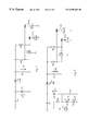
- FIG. 1 a principle of or circuit diagram of a capacitive bridge circuit with evaluation according to the present invention.
- FIG. 2 to the principle of a circuit diagram of FIG. 1 supplemented by in each case a low pass filter in front of the rectifiers.
- FIG. 8 the circuit diagram of FIG. 7 stranded by N 5 , N 6 , R 8 , C 10 , and Uv for showing that the rectified voltage Ugl is independent of the forward flow voltage Uf of the rectifier diodes.
- FIG. 10 a principle of a construction of a capacitive proximity switch with the formation of the capacitances of one bridge branch by different layers of amount the layer circuit board in combination with their environment.
- bridge half means—graphically in the figures—the left or, respectively right hand side or, respectively, half of the bridge, with ‘bridge branch’ being the switching part between the two switching knots such that a bridge includes two ‘halves’ and four ‘branches’ or, respectively, ‘bridge branches’.
- FIG. 1 shows a principle circuit diagram of a capacitive electrical bridge circuit according to the present invention, such as capacitive electrical bridge circuit can be employed for constructing of a capacitive proximity switch comprising the bridge with in each case a capacitance C 1 , C 2 , C 3 , and C 4 in each bridge branch; the capacitance C 1 is variable.
- the bridge is fed by the bridge feed voltage ubr, wherein the bridge feed voltage is an alternating voltage; the reference potential is ground GND.
- the two bridge branch voltages uc 1 and uc 3 from the two bridge halves are rectified separately according to the respective bridge branch with the diodes N 2 , N 1 or, respectively, N 4 , N 3 disposed in the diagonal voltage paths DSp 1 and DSp 2 and are smoothed in each case relative to ground with capacitors C 5 , C 6 as well as resistances R 1 and R 2 , whereupon the bridge diagonal voltage Ud is evaluated as a direct voltage changing corresponding to the change of the capacitance C 1 .
- Plus the bridge diagonal voltage of the diagonal voltage paths DSp 1 and DSp 2 is obtained only after rectification of the two bridge branch voltages uc 1 and uc 3 as a difference voltage Ud, that means according to FIG. 1 as a rectified voltage U out of udiff+ ⁇ udiff ⁇ .
- FIG. 2 shows the principle circuit diagram of FIG. 1 supplemented in each case by a low pass filter in each bridge branch in front of the rectifires N 2 , N 1 , N 4 , N 3 for suppressing of coupled in interferences, formed by the resistances R 3 and R 4 disposed in the diagonal paths Dsp 1 and DSp 2 for coupling out of the two bridge branch voltages uc 1 and uc 3 as well as the capacitors C 7 , C 8 .
- the capacitors C 7 and C 8 of the low pass filter R 3 -C 8 as well as R 4 -C 7 can also be formed by the parasitic capacitances of the elements of the rectifier N 1 , N 2 , N 3 , N 4 .
- FIG. 3 shows a further principle circuit diagram, wherein the rectifier diodes are replaced by electronic switches S 2 , S 1 or, respectively, S 4 , S 3 .
- the two switches S 2 , S 4 disposed in the respective de-coupling lines of the bridge branches are addressed and closed as well as opened by the control voltage Ust 2
- the two switches S 1 , S 3 disposed against ground are addressed and closed as well as opened by the control voltage Ust 1 .
- These switches are pairwise opposite phase controlled.
- the capacitances of the respective low pass filters can be formed by parasitic capacitances of the elements of these switches S 1 , S 2 , S 3 , S 4 even upon employment of switches and low pass filters.
- FIG. 5 shows a principle circuit diagram for setting for example the zero point of the bridge diagonal voltage Ud with two reference voltage sources Uref 1 and Uref 2 .
- the values of the reference voltage source Uref 1 , Uref 2 are adjusted such that the desired bridge diagonal voltage Ud is set at the output.
- FIG. 6 shows the employment of diodes as rectifier elements in FIG. 5, wherein the diodes exhibit the threshold voltage Uf. Then they result of the following relationships:
- ubr is the peak-peak-value of the bridge feed voltage. If in contrast the diodes are connected on the cathode side in each case to a reference voltage different from zero, then one obtains
- the circuit according to the present invention can also be constructed with a bridge, wherein the bridge comprises two capacitors and two resistors in each bridge branch, which is shown in principle in FIG. 9.
- a capacitive bridge circuit with in each case a capacitance C 1 and C 2 as well as in each case an ohmic resistor R 9 , R 10 in each bridge branch is shown in FIG. 9 .
- the corresponding bridge branch voltage has to be decoupled through a capacitor C 11 in the bridge half constructed with the resistors R 9 , R 10 , otherwise the bridge corresponds to the about describe FIG. 1 .
- the describe circuit arrangement is in particular suited for the construction of the capacitive proximity switch for detecting of a face 15 approaching or moving away, for example of an electrically bad conductive face or a metal face.
- FIG. 10 shows a principal construction of such a capacitive proximity switch, which represents 1 ⁇ 2 of the bridge, with the formation of capacitances over bridge branch by various layers of a flat multilayer circuit board 10 in combination with its surroundings.
- the multilayer printed circuit board 10 comprises at least two electrically insulating layers 13 , 14 , wherein an electrically conducting intermediate layer 11 , for example a metallic intermediate layer, is disposed as a first face of a capacitor between the electrically insulating layers 13 , 14 .
- a flat, also electrically conducting covering is applied as a sense of 12 on one of the two layers 13 or, respectively, 14 , namely here of the upper layers 13 , wherein the sensor 12 forms the second face of the capacitor, wherein the face 15 , that is in particular an electrically bad conductive face or metal face, is disposed movable relative to the sensor 12 and wherein the face 15 together with the sensor 12 forms the second flat, variable capacitor with for example air as a dielectric.
- the face 15 can also be grounded by way of a conduit 17 .
- the face 15 together with the sensor 12 for my capacity of the one bridge half, the sensor 12 and the metallic layer 11 form the second capacitance of the same bridge half; this construction represents the one half of the bridge.
- Further electrical device elements 16 are placed on the side of the multilayer printed circuit board 10 disposed opposite to the sensor 12 and to thus on the lower electrically insulating layer 14 .
- the capacitor face formed by the electrically conducting intermediate layer 11 can also be exchanged by a discrete capacitor, which discrete capacitor is connected with a connector to the sensor 12 .
- a discrete capacitor which discrete capacitor is connected with a connector to the sensor 12 .
- An intermediate layer or a shielding, such as for example the electrically conducting intermediate layer 11 therefore should always then be provided in case the proximity switch is thinner in its thickness construction as the region of influence of the proximity switch.
- the subject matter of the present invention is suitable in particular for employment as a highly sensitive capacitive proximity switch.
- the usefulness of the proximity switch according to the present invention comprises in particular that the proximity switch is on the one side highly sensitive relative to the approach of an object, however, is for practical purposes insensitive against such an approach on the oppositely disposed side.
Landscapes
- Physics & Mathematics (AREA)
- Engineering & Computer Science (AREA)
- Remote Sensing (AREA)
- Life Sciences & Earth Sciences (AREA)
- Electromagnetism (AREA)
- Environmental & Geological Engineering (AREA)
- Geology (AREA)
- General Life Sciences & Earth Sciences (AREA)
- General Physics & Mathematics (AREA)
- Geophysics (AREA)
- Electronic Switches (AREA)
- Switches That Are Operated By Magnetic Or Electric Fields (AREA)
Applications Claiming Priority (7)
| Application Number | Priority Date | Filing Date | Title |
|---|---|---|---|
| DE19834891 | 1998-08-03 | ||
| DE19834891 | 1998-08-03 | ||
| DE19842189 | 1998-09-15 | ||
| DE19842189 | 1998-09-15 | ||
| DE19843749 | 1998-09-24 | ||
| DE19843749A DE19843749A1 (de) | 1998-08-03 | 1998-09-24 | Verfahren und Schaltungsanordnung zur Auswertung kleiner Kapazitätsänderungen |
| PCT/EP1999/005559 WO2000008487A1 (fr) | 1998-08-03 | 1999-08-02 | Commutateur capacitif destine a l'evaluation de changements minimes de la capacite et procede associe |
Publications (1)
| Publication Number | Publication Date |
|---|---|
| US6590401B1 true US6590401B1 (en) | 2003-07-08 |
Family
ID=27218561
Family Applications (1)
| Application Number | Title | Priority Date | Filing Date |
|---|---|---|---|
| US09/762,356 Expired - Fee Related US6590401B1 (en) | 1998-08-03 | 1999-08-02 | Capacitive proximity switch for evaluating minor changes in capacitance and method therefor |
Country Status (6)
| Country | Link |
|---|---|
| US (1) | US6590401B1 (fr) |
| EP (1) | EP1103007B1 (fr) |
| AU (1) | AU779212B2 (fr) |
| CA (1) | CA2339535C (fr) |
| ES (1) | ES2212851T3 (fr) |
| WO (1) | WO2000008487A1 (fr) |
Cited By (6)
| Publication number | Priority date | Publication date | Assignee | Title |
|---|---|---|---|---|
| US20030009273A1 (en) * | 1998-12-30 | 2003-01-09 | Automotive Systems Laboratory, Inc. | Occupant Detection System |
| US20060255266A1 (en) * | 2005-05-13 | 2006-11-16 | Alison Chaiken | System for repositioning a microfabricated cantilever |
| US20080117840A1 (en) * | 2002-10-10 | 2008-05-22 | Christian Fleischhacker | Bridge Circuit to Suppress Echoes in Communication Devices |
| US20090033340A1 (en) * | 2007-08-03 | 2009-02-05 | Pepperl + Fuchs, Inc. | System and method for high resolution sensing of capacitance or other reactive impedance change in a large dynamic range |
| WO2009026912A1 (fr) * | 2007-08-30 | 2009-03-05 | Micro-Epsilon Messtechnik Gmbh & Co. Kg | Protection anti-pincement capacitive et procédé pour faire fonctionner une protection anti-pincement |
| US12510682B2 (en) * | 2023-09-08 | 2025-12-30 | Cypress Semiconductor Corporation | Precise proximity object detection for capacitive sensing |
Citations (6)
| Publication number | Priority date | Publication date | Assignee | Title |
|---|---|---|---|---|
| US3694741A (en) | 1970-10-28 | 1972-09-26 | Ade Corp | Coupled inductance impedance measuring circuit with increased sensitivity and frequency independence |
| FR2371676A1 (fr) | 1976-11-18 | 1978-06-16 | Mitsubishi Electric Corp | Detecteur de proximite |
| EP0564164A1 (fr) | 1992-04-01 | 1993-10-06 | AT&T Corp. | Capteurs de proximité capacitives |
| US5442347A (en) * | 1993-01-25 | 1995-08-15 | The United States Of America As Represented By The Administrater, National Aeronautics & Space Administration | Double-driven shield capacitive type proximity sensor |
| US5539292A (en) * | 1994-11-28 | 1996-07-23 | The United States Of America As Represented By The Administrator Of The National Aeronautics And Space Administration | Capaciflector-guided mechanisms |
| DE19701899A1 (de) | 1996-01-21 | 1997-10-30 | Ifm Electronic Gmbh | Schaltungsanordnung zur Erfassung der Kapazität bzw. einer Kapazitätsänderung eines kapazitiven Schaltungs- oder Bauelementes |
-
1999
- 1999-08-02 ES ES99941498T patent/ES2212851T3/es not_active Expired - Lifetime
- 1999-08-02 CA CA002339535A patent/CA2339535C/fr not_active Expired - Fee Related
- 1999-08-02 EP EP99941498A patent/EP1103007B1/fr not_active Expired - Lifetime
- 1999-08-02 WO PCT/EP1999/005559 patent/WO2000008487A1/fr not_active Ceased
- 1999-08-02 US US09/762,356 patent/US6590401B1/en not_active Expired - Fee Related
- 1999-08-02 AU AU55092/99A patent/AU779212B2/en not_active Ceased
Patent Citations (6)
| Publication number | Priority date | Publication date | Assignee | Title |
|---|---|---|---|---|
| US3694741A (en) | 1970-10-28 | 1972-09-26 | Ade Corp | Coupled inductance impedance measuring circuit with increased sensitivity and frequency independence |
| FR2371676A1 (fr) | 1976-11-18 | 1978-06-16 | Mitsubishi Electric Corp | Detecteur de proximite |
| EP0564164A1 (fr) | 1992-04-01 | 1993-10-06 | AT&T Corp. | Capteurs de proximité capacitives |
| US5442347A (en) * | 1993-01-25 | 1995-08-15 | The United States Of America As Represented By The Administrater, National Aeronautics & Space Administration | Double-driven shield capacitive type proximity sensor |
| US5539292A (en) * | 1994-11-28 | 1996-07-23 | The United States Of America As Represented By The Administrator Of The National Aeronautics And Space Administration | Capaciflector-guided mechanisms |
| DE19701899A1 (de) | 1996-01-21 | 1997-10-30 | Ifm Electronic Gmbh | Schaltungsanordnung zur Erfassung der Kapazität bzw. einer Kapazitätsänderung eines kapazitiven Schaltungs- oder Bauelementes |
Cited By (11)
| Publication number | Priority date | Publication date | Assignee | Title |
|---|---|---|---|---|
| US20030009273A1 (en) * | 1998-12-30 | 2003-01-09 | Automotive Systems Laboratory, Inc. | Occupant Detection System |
| US6825765B2 (en) | 1998-12-30 | 2004-11-30 | Automotive Systems Laboratory, Inc. | Occupant detection system |
| US20080117840A1 (en) * | 2002-10-10 | 2008-05-22 | Christian Fleischhacker | Bridge Circuit to Suppress Echoes in Communication Devices |
| US7778210B2 (en) * | 2002-10-10 | 2010-08-17 | Infineon Technologies, Ag | Bridge circuit to suppress echoes in communication devices |
| US20060255266A1 (en) * | 2005-05-13 | 2006-11-16 | Alison Chaiken | System for repositioning a microfabricated cantilever |
| US7372026B2 (en) * | 2005-05-13 | 2008-05-13 | Hewlett-Packard Development Company, L.P. | System for repositioning a microfabricated cantilever |
| US20090033340A1 (en) * | 2007-08-03 | 2009-02-05 | Pepperl + Fuchs, Inc. | System and method for high resolution sensing of capacitance or other reactive impedance change in a large dynamic range |
| US7663377B2 (en) | 2007-08-03 | 2010-02-16 | Pepperl +Fuchs, Inc. | System and method for high resolution sensing of capacitance or other reactive impedance change in a large dynamic range |
| WO2009026912A1 (fr) * | 2007-08-30 | 2009-03-05 | Micro-Epsilon Messtechnik Gmbh & Co. Kg | Protection anti-pincement capacitive et procédé pour faire fonctionner une protection anti-pincement |
| US20100244860A1 (en) * | 2007-08-30 | 2010-09-30 | Karl Wisspeintner | Capacitive anti-pinch means and method for operating an anti-pinch means |
| US12510682B2 (en) * | 2023-09-08 | 2025-12-30 | Cypress Semiconductor Corporation | Precise proximity object detection for capacitive sensing |
Also Published As
| Publication number | Publication date |
|---|---|
| WO2000008487A1 (fr) | 2000-02-17 |
| AU779212B2 (en) | 2005-01-13 |
| CA2339535C (fr) | 2004-01-27 |
| ES2212851T3 (es) | 2004-08-01 |
| EP1103007A1 (fr) | 2001-05-30 |
| EP1103007B1 (fr) | 2003-09-17 |
| CA2339535A1 (fr) | 2000-02-17 |
| AU5509299A (en) | 2000-02-28 |
Similar Documents
| Publication | Publication Date | Title |
|---|---|---|
| US6194903B1 (en) | Circuit for acquisition of the capacitance or capacitance change of a capacitive circuit element or component | |
| US8587329B2 (en) | Circuit arrangement for determination of a measuring capacitance | |
| US9401697B2 (en) | Device for generating an alternating voltage difference between the reference potentials of electronic systems | |
| US8041534B2 (en) | Sensor device, and sensor system and electronic device using the sensor device | |
| US9442143B2 (en) | Capacitive proximity sensor as well as method for capacitive approximation detection | |
| US6031430A (en) | Temperature stabilized oscillator and proximity switch containing the oscillator | |
| WO2002063323A3 (fr) | Procede et appareil pour tester un circuit integre par l'intermediaire d'un couplage capacitif | |
| US6590401B1 (en) | Capacitive proximity switch for evaluating minor changes in capacitance and method therefor | |
| US11003280B2 (en) | Switching operation sensing apparatus with low-power dual-sensing structure | |
| EP0079955B1 (fr) | Circuit de mesure de l'impedance | |
| US4410812A (en) | Voltage-frequency converter | |
| US6777956B2 (en) | Capacitance measuring systems | |
| US7260987B2 (en) | Method for capacitive measurement of fill level | |
| US6674333B1 (en) | Band switchable voltage controlled oscillator with substantially constant tuning range | |
| US4195274A (en) | Temperature compensating circuit for varactor diodes | |
| US8044669B2 (en) | Admittance meter for monitoring a medium | |
| US11456739B2 (en) | Assembly for a capacitive sensor device | |
| EP4191243A2 (fr) | Appareil de détection d'état d'huile | |
| US6323660B1 (en) | Integrated device for capacitive measuring of nanometer distances | |
| US11847854B2 (en) | Optical fingerprint sensing system with common mode compensation | |
| US6867605B2 (en) | Circuit for determining the internal resistance of a linear lambda probe | |
| KR101897150B1 (ko) | 지문 검출 장치 및 방법 | |
| KR100217418B1 (ko) | 전압제어발진기의 주파수 조정회로 | |
| JPH0233410Y2 (fr) | ||
| JPH10173519A (ja) | 自動移相回路 |
Legal Events
| Date | Code | Title | Description |
|---|---|---|---|
| AS | Assignment |
Owner name: PEPPERL & FUCHS GMBH, GERMANY Free format text: ASSIGNMENT OF ASSIGNORS INTEREST;ASSIGNOR:HILDEBRANDT, ANDREAS;REEL/FRAME:011685/0298 Effective date: 20010330 |
|
| FPAY | Fee payment |
Year of fee payment: 4 |
|
| FPAY | Fee payment |
Year of fee payment: 8 |
|
| SULP | Surcharge for late payment | ||
| REMI | Maintenance fee reminder mailed | ||
| LAPS | Lapse for failure to pay maintenance fees | ||
| STCH | Information on status: patent discontinuation |
Free format text: PATENT EXPIRED DUE TO NONPAYMENT OF MAINTENANCE FEES UNDER 37 CFR 1.362 |
|
| STCH | Information on status: patent discontinuation |
Free format text: PATENT EXPIRED DUE TO NONPAYMENT OF MAINTENANCE FEES UNDER 37 CFR 1.362 |
|
| FP | Lapsed due to failure to pay maintenance fee |
Effective date: 20150708 |