US7324717B2 - Photonic device with integrated hybrid microlens array - Google Patents
Photonic device with integrated hybrid microlens array Download PDFInfo
- Publication number
- US7324717B2 US7324717B2 US11/286,123 US28612305A US7324717B2 US 7324717 B2 US7324717 B2 US 7324717B2 US 28612305 A US28612305 A US 28612305A US 7324717 B2 US7324717 B2 US 7324717B2
- Authority
- US
- United States
- Prior art keywords
- light emitting
- microlens
- detecting
- vcsel
- pedestal
- Prior art date
- Legal status (The legal status is an assumption and is not a legal conclusion. Google has not performed a legal analysis and makes no representation as to the accuracy of the status listed.)
- Expired - Lifetime, expires
Links
Images



Classifications
-
- H—ELECTRICITY
- H10—SEMICONDUCTOR DEVICES; ELECTRIC SOLID-STATE DEVICES NOT OTHERWISE PROVIDED FOR
- H10F—INORGANIC SEMICONDUCTOR DEVICES SENSITIVE TO INFRARED RADIATION, LIGHT, ELECTROMAGNETIC RADIATION OF SHORTER WAVELENGTH OR CORPUSCULAR RADIATION
- H10F77/00—Constructional details of devices covered by this subclass
- H10F77/40—Optical elements or arrangements
- H10F77/413—Optical elements or arrangements directly associated or integrated with the devices, e.g. back reflectors
-
- H—ELECTRICITY
- H01—ELECTRIC ELEMENTS
- H01S—DEVICES USING THE PROCESS OF LIGHT AMPLIFICATION BY STIMULATED EMISSION OF RADIATION [LASER] TO AMPLIFY OR GENERATE LIGHT; DEVICES USING STIMULATED EMISSION OF ELECTROMAGNETIC RADIATION IN WAVE RANGES OTHER THAN OPTICAL
- H01S5/00—Semiconductor lasers
- H01S5/02—Structural details or components not essential to laser action
- H01S5/022—Mountings; Housings
- H01S5/0225—Out-coupling of light
- H01S5/02257—Out-coupling of light using windows, e.g. specially adapted for back-reflecting light to a detector inside the housing
-
- H—ELECTRICITY
- H01—ELECTRIC ELEMENTS
- H01S—DEVICES USING THE PROCESS OF LIGHT AMPLIFICATION BY STIMULATED EMISSION OF RADIATION [LASER] TO AMPLIFY OR GENERATE LIGHT; DEVICES USING STIMULATED EMISSION OF ELECTROMAGNETIC RADIATION IN WAVE RANGES OTHER THAN OPTICAL
- H01S5/00—Semiconductor lasers
- H01S5/10—Construction or shape of the optical resonator, e.g. extended or external cavity, coupled cavities, bent-guide, varying width, thickness or composition of the active region
- H01S5/18—Surface-emitting [SE] lasers, e.g. having both horizontal and vertical cavities
- H01S5/183—Surface-emitting [SE] lasers, e.g. having both horizontal and vertical cavities having only vertical cavities, e.g. vertical cavity surface-emitting lasers [VCSEL]
- H01S5/18386—Details of the emission surface for influencing the near- or far-field, e.g. a grating on the surface
- H01S5/18388—Lenses
-
- H—ELECTRICITY
- H10—SEMICONDUCTOR DEVICES; ELECTRIC SOLID-STATE DEVICES NOT OTHERWISE PROVIDED FOR
- H10W—GENERIC PACKAGES, INTERCONNECTIONS, CONNECTORS OR OTHER CONSTRUCTIONAL DETAILS OF DEVICES COVERED BY CLASS H10
- H10W72/00—Interconnections or connectors in packages
- H10W72/50—Bond wires
- H10W72/541—Dispositions of bond wires
- H10W72/5449—Dispositions of bond wires not being orthogonal to a side surface of the chip, e.g. fan-out arrangements
-
- H—ELECTRICITY
- H10—SEMICONDUCTOR DEVICES; ELECTRIC SOLID-STATE DEVICES NOT OTHERWISE PROVIDED FOR
- H10W—GENERIC PACKAGES, INTERCONNECTIONS, CONNECTORS OR OTHER CONSTRUCTIONAL DETAILS OF DEVICES COVERED BY CLASS H10
- H10W72/00—Interconnections or connectors in packages
- H10W72/851—Dispositions of multiple connectors or interconnections
- H10W72/874—On different surfaces
- H10W72/884—Die-attach connectors and bond wires
-
- H—ELECTRICITY
- H10—SEMICONDUCTOR DEVICES; ELECTRIC SOLID-STATE DEVICES NOT OTHERWISE PROVIDED FOR
- H10W—GENERIC PACKAGES, INTERCONNECTIONS, CONNECTORS OR OTHER CONSTRUCTIONAL DETAILS OF DEVICES COVERED BY CLASS H10
- H10W90/00—Package configurations
- H10W90/701—Package configurations characterised by the relative positions of pads or connectors relative to package parts
- H10W90/731—Package configurations characterised by the relative positions of pads or connectors relative to package parts of die-attach connectors
- H10W90/734—Package configurations characterised by the relative positions of pads or connectors relative to package parts of die-attach connectors between a chip and a stacked insulating package substrate, interposer or RDL
-
- H—ELECTRICITY
- H10—SEMICONDUCTOR DEVICES; ELECTRIC SOLID-STATE DEVICES NOT OTHERWISE PROVIDED FOR
- H10W—GENERIC PACKAGES, INTERCONNECTIONS, CONNECTORS OR OTHER CONSTRUCTIONAL DETAILS OF DEVICES COVERED BY CLASS H10
- H10W90/00—Package configurations
- H10W90/701—Package configurations characterised by the relative positions of pads or connectors relative to package parts
- H10W90/751—Package configurations characterised by the relative positions of pads or connectors relative to package parts of bond wires
- H10W90/754—Package configurations characterised by the relative positions of pads or connectors relative to package parts of bond wires between a chip and a stacked insulating package substrate, interposer or RDL
Definitions
- This invention relates to light emitting and light detecting integrated circuit (IC) devices, and more particularly to assemblies that include microlens arrays positioned to focus light into or out of light emitting/detecting (photonic) IC devices.
- IC integrated circuit
- High-speed printers utilize multiple-beam semiconductor lasers that are capable of transferring print data in parallel.
- the printing speed of such a high-speed printer is in part limited by the laser intensity (output power) and number of parallel laser beams of the printer's multiple-beam semiconductor laser.
- Early laser-based high-speed printers utilized edge-emitting devices, which emit light parallel to the various layers formed during fabrication (i.e., parallel the upper surface of the device “chip”). A problem with edge-emitting devices is that the number of laser beams that can practically be included in a multiple-beam laser array is four.
- VCSELs Vertical Cavity Surface Emitting Lasers
- VCSELs Vertical Cavity Surface Emitting Lasers
- a problem associated with the use of VCSELs in high-speed printers is that they have inherently low output power, thus requiring more time for each beam to transfer sufficient energy.
- FIG. 10 illustrates an exemplary architecture including microlenses fabricated on a “backside” surface of a substrate (i.e., opposite to the “top” surface on which the VCSELs are fabricated).
- This approach while attractive for some applications, has significant limitations.
- the lens diameter and spacing are necessarily large (on the order of a few hundred microns).
- the thickness of the substrate is difficult to control precisely, so the z-displacement tolerance of the lens relative to the light source position is substantial.
- the substrate has to be transparent to the wavelength of interest.
- the lens fabrication steps, including substrate backside processing have to be compatible with those of the lasers.
- the present invention is directed to an integrated photonic device/microlens assembly that is produced using a hybrid approach in which a microlens structure and a photonic (e.g., VCSEL) device are produced separately, and then assembled using precision alignment equipment such that microlens structure is mounted directly onto the VCSEL device. Because the components (e.g., the VCSEL device and microlens structure) are separately produced, the hybrid approach utilized by the present invention allows the components to be manufactured in a cost effective manner and separately designed and manufactured for optimized performance, thus facilitating the economical production of VCSEL-based printing systems.
- a hybrid approach in which a microlens structure and a photonic (e.g., VCSEL) device are produced separately, and then assembled using precision alignment equipment such that microlens structure is mounted directly onto the VCSEL device. Because the components (e.g., the VCSEL device and microlens structure) are separately produced, the hybrid approach utilized by the present invention allows the components to be manufactured in a cost effective manner and separately designed
- the microlens structure includes a microlens array and three or more stand-off structures (legs) that extend from the lower surface of a transparent (e.g., glass) block-like pedestal.
- the microlens array is centrally located on the lower surface, with each microlens extending a relatively small distance from the pedestal's lower surface.
- the legs are located adjacent to a peripheral edge of the lower surface and extend a relatively large distance from the lower surface.
- the microlens structure is mounted onto the upper surface of a light emitting/detecting device that includes a semiconductor substrate (chip) having a substantially planar upper surface, an array of light emitting/detecting elements fabricated on the substrate and located in a central region of the upper surface, and a plurality of contact pads that are located around a periphery of the upper surface and connected to the light emitting/detecting elements by conductive lines formed on the substrate.
- a semiconductor substrate chip having a substantially planar upper surface, an array of light emitting/detecting elements fabricated on the substrate and located in a central region of the upper surface, and a plurality of contact pads that are located around a periphery of the upper surface and connected to the light emitting/detecting elements by conductive lines formed on the substrate.
- the microlens structure is produced such that, when the pedestal is mounted onto the upper surface of the light emitting/detecting device, each microlens is operably positioned over a corresponding light emitting/detecting element (i.e., such that light emitted from a light emitting element is collected and directed in a predetermined manner by the corresponding microlens, or light passing through each microlens is focused onto a corresponding light receiving element).
- a corresponding light emitting/detecting element i.e., such that light emitted from a light emitting element is collected and directed in a predetermined manner by the corresponding microlens, or light passing through each microlens is focused onto a corresponding light receiving element.
- the legs contact surface regions of the substrate that are laterally located between the contact pads and light emitting/detecting elements.
- the microlens structure is supported directly on the upper surface of the light emitting/detecting device, the microlens array is maintained at a distance from the underlying light emitting/detecting elements that is determined by the length of the legs. Accordingly, the hybrid arrangement facilitates precise positioning of the microlenses relative to their associated light emitting/detecting elements. Further, by mounting the legs directly onto the upper surface of the substrate, the lower surface of the pedestal is self-aligned to the upper surface of the substrate (i.e., both planar surfaces are automatically positioned and maintained parallel to each other), thereby automatically positioning each microlens of the microlens array at an optimal distance above its corresponding light emitting/detecting element.
- a VCSEL device is mounted inside a conventional IC package, and the microlens structure includes a carrier plate that is connected to peripheral walls of the IC package, with the block-like pedestal extending from the carrier plate and contacting the VCSEL device in the manner described above.
- the VCSEL device is soldered into a central chamber of the IC package structure using conventional techniques, and the peripheral contact pads of the VCSEL device are connected, for example, by conventional wirebonding techniques to corresponding contacts formed on stepped shelves (ledges) of the IC package structure surrounding the central chamber.
- the microlens structure is mounted onto the VCSEL device such that the pedestal's legs contact the upper surface of the VCSEL device in the manner described above.
- the hybrid arrangement of the present invention facilitates automatic self-alignment of the distances between the microlens array and the underlying VCSEL array.
- the carrier plate is then secured to the peripheral walls of the package structure using a suitable adhesive.
- the relatively large carrier plate facilitates manipulation and fine positioning of the microlens array, and also serves as a cover plate to seal protect the VCSEL device inside the central chamber of the IC package.
- the carrier plate is transparent to ultraviolet (UV) light, and is secured to the IC package structure by a UV-activated adhesive.
- UV ultraviolet
- the present invention is also directed to a method for integrating microlenses onto VCSEL arrays using the hybrid approach mentioned above.
- the method includes separately producing the block-like pedestal, the carrier plate, the VCSEL device and the IC package structure, which as mentioned above both reduces production costs and facilitates optimization of the separate components.
- the microlenses and legs are integrally (monolithically) fabricated by, for example, etching the pedestal material, which in one embodiment is glass. Intersecting grooves are cut in the upper and lower surfaces of the carrier plate that intersect in a central region of the plate, thereby forming a through-hole that is sized to receive the pedestal, which is attached using an adhesive to complete the microlens structure.
- a base of the pedestal is then mounted and secured inside the through-hole such that the lower surface of the pedestal protrudes away from the carrier plate.
- the VCSEL device is soldered onto the IC package structure as described above.
- the IC package structure is then mounted onto a movable stage, and the microlens structure is mounted onto a suspension frame and positioned over the VCSEL device.
- a suitable adhesive is applied to the IC package and/or the VCSEL device.
- a microscope is utilized in conjunction with the movable stage and suspension frame to finely position the microlens array over the VCSEL array.
- the VCSEL device/package is then lifted (or the microlens structure is then lowered onto the VCSEL device) such that the pedestal legs contact the upper surface of the VCSEL device and the microlens structure becomes fully supported by the VCSEL device.
- Slight tilt variations of the VCSEL relative to the IC package structure arise due to the soldering operation used to secure the VCSEL device onto the IC package.
- the present invention facilitates automatic self-alignment of the microlens structure to the particular tilt angle of each VCSEL device.
- the adhesive is then activated (e.g., by transmitting UV light through the carrier plate), whereby the peripheral edge of the carrier plate is secured to the IC package structure and/or the microlens structure is secured to the VCSEL device.
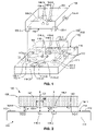
- FIG. 1 is a top side perspective view showing an assembly including a microlens structure and a light emitting/detecting device according to a generalized embodiment of the present invention
- FIG. 2 is a simplified cross-sectional side view showing the assembly of FIG. 1 ;
- FIG. 3 is an exploded perspective view showing an assembly including a microlens structure, a VCSEL device and IC package according to another embodiment of the present invention
- FIG. 4 is a simplified cross-sectional side view showing the assembly of FIG. 3 ;
- FIG. 5 is a flow diagram showing a method for producing the assembly of FIG. 3 ;
- FIG. 6 is a photograph showing a-pedestal including a microlens array and stand-offs (legs) according to a practical embodiment of the present invention
- FIG. 7 is a perspective view showing a simplified carrier plate formed in accordance with another embodiment of the present invention.
- FIG. 8 is a photograph showing an assembled microlens structure according to a practical embodiment of the present invention.
- FIG. 9 is an exploded perspective view showing a simplified arrangement for producing VCSEL assemblies according to another embodiment of the present invention.
- FIG. 10 is a simplified cross-sectional side view showing a VCSEL array with a conventional integrated microlens array.
- the present invention relates to a hybrid arrangement for mounting microlenses over IC-based light emission/detection devices.
- the hybrid arrangement disclosed herein may also be used in other IC-based light-emission device arrays such as light emitting diodes, and may also be utilized in IC-based light detection device arrays such as p-i-n photodetectors, resonant cavity sensors, metal-semiconductor-metal detectors, and avalanche photodetectors.
- the term “light emitting/detecting IC device” or “photonic device” is utilized herein to refer to either of these device types.
- FIG. 1 is an exploded perspective view showing a VCSEL apparatus 100 including a VCSEL device 110 and a microlens structure 150 .
- Microlens structure 150 is shown both in solid lines above VCSEL device 110 , and in dashed lines in a mounted position on VCSEL device 110 .
- VCSEL device 110 is a conventional IC device that is fabricated according to known semiconductor fabricating techniques, and generally includes a semiconductor substrate 111 having a substantially planar upper surface 112 , and at least one VCSEL located in a central region of upper surface 112 (four VCSEL elements 118 - 1 to 118 - 4 are indicated in FIG. 1 , and are collectively referred to below as VCSELs 118 or VCSEL array 118 ).
- VCSELs 118 are fabricated on or below upper surface 112 of substrate 111 such that light beams generated by VCSELs 118 are predominantly emitted upward from upper surface 112 .
- VCSEL device 110 also includes contact pads 113 that are arranged around a peripheral edge of upper surface 112 .
- Contact pads 113 are electrically connected to VCSELs 115 by way of conductive lines 114 , which are formed according to known “backside” techniques. Conductive lines 114 are typically covered with an insulating material (e.g., silicon dioxide), but contact pads are exposed on upper surface 112 to facilitate connection by conventional wire bonding techniques to a IC package.
- conductive lines 114 are typically covered with an insulating material (e.g., silicon dioxide), but contact pads are exposed on upper surface 112 to facilitate connection by conventional wire bonding techniques to a IC package.
- Microlens structure 150 includes a monolithic, transparent, block-like pedestal 151 having a substantially planar lower surface 152 . At least one microlens is integrally fabricated in a central region of lower surface 152 , and extends a relatively small distance from lower surface 152 (four microlenses 158 - 1 to 158 - 4 are indicated in FIG. 1 , and are collectively referred to below as microlenses 158 or microlens array 158 ).
- pedestal 151 includes three or more “stand-off” legs that are, in one embodiment, integrally fabricated along the peripheral edges of lower surface 152 , and extend a relatively large distance from lower surface 152 (four legs 155 - 1 to 155 - 4 are indicated in FIG.
- legs 155 are collectively referred to below as legs 155 ).
- the terms “monolithic” and “integrally fabricated” are intended to convey that these structures are chemically etched, reactive ion etched, ion milled, plasma etched, molded, photo-defined or otherwise micromachined (defined) in the single block of light-transparent material (e.g., glass, sapphire, plastic, polymer, acrylic or quartz) that makes up pedestal 151 .
- the stand-off legs can also be a different material that is deposited and formed on the pedestal by, for example, screen printing, spin-coat or spray-coat deposition.
- pedestal 151 is mounted onto upper surface 112 of VSEL device 110 such that each leg (e.g., legs 155 - 1 and 155 - 2 ) contacts a corresponding region (e.g., surface regions 112 - 1 and 112 - 2 ) of upper surface 112 .
- each leg e.g., legs 155 - 1 and 155 - 2
- a corresponding region e.g., surface regions 112 - 1 and 112 - 2
- each microlens 158 e.g., microlenses 158 - 1 and 158 - 2 , as shown in FIG. 2
- Microlenses 158 are fabricated to be substantially identical (e.g., to have a common diameter D and produce substantially the same optical characteristics), and are arranged in a pattern that matches the arrangement of VCSEL elements 118 on upper surface 112 .
- the distance Z 1 is determined by the optical characteristics of microlenses 158 and the intensity of light beams LB (depicted in a simplified manner by dashed arrows in FIG. 2 ) emitted (or received) by VCSEL elements 118 .
- each of the legs 155 with the common length Hi and mounting pedestal 151 onto upper surface 112 such that all of the legs 155 contact a corresponding region of upper surface 112 , all of the microlenses 155 can be automatically precisely positioned at the optimal predetermined distance Z 1 from its corresponding VCSEL element 118 , thereby significantly improving the amount of light transmitted along the optical axis of each VCSEL element 118 .
- the microlens structure 150 is mounted onto upper surface 112 of VCSEL device 110 such that the corresponding regions (e.g., regions 112 - 1 and 112 - 2 ) are located between the peripherally positioned contact pads 113 and the centrally located VCSEL elements 118 .
- regions 112 - 1 and 112 - 2 are located between the peripherally positioned contact pads 113 and the centrally located VCSEL elements 118 .
- “located between” is intended in a concentric sense (e.g., as indicated in FIG. 1 , an imaginary line Ll linking regions 112 - 1 and 112 - 2 surrounds VCSEL elements 118 , and is located inside an imaginary line L 2 linking contact pads 113 ).
- microlens structure 150 inboard of the contact structures facilitates wire bond contacts to VCSEL device 110 .
- the photonic integrated circuit is fully wired and electrically active before the lens is assembled. This approach allows the IC to be tested and sorted so that only devices that meet all performance specifications are considered for the value added lens retrofit steps.
- the photonic integrated circuit needs to be activated during the alignment process to produce a signal. The position where maximum signal levels are reached would indicate optimal alignment. Therefore, it is important that the structures and methods for integrating photonic elements with microlens arrays allow the photonic elements to be electrically activated before lens alignment.
- FIGS. 3 and 4 are perspective and cross-sectional side views showing a VCSEL assembly 200 according to a practical embodiment of the present invention.
- VCSEL assembly 200 generally includes a VCSEL structure 210 and a microlens structure 250 . Structures that are the same or substantially similar to corresponding structures of the embodiment described above are identified with the same or similar reference numbers.
- VCSEL structure 210 includes VCSEL device 110 (described above) that is mounted inside a conventional IC package 220 .
- IC package 220 includes a laminated body 221 defining a central cavity 222 .
- VCSEL device 110 is mounted inside cavity 222 in the manner depicted in FIG. 3 , and is secured onto a lower inside surface 225 of IC package 220 by way of a solder structure 230 , as indicated in FIG. 4 .
- FIG. 3 indicates contact pads of VCSEL device 110 are electrically connected to internal contact pads located inside cavity 222 by way of wire bonds 240 .
- FIG. 4 shows exemplary internal contact pads 223 of IC package 220 , which are formed on a stepped shelf 224 inside cavity 222 .
- Each internal contact pad 223 is connected to a corresponding contact pad 113 of VCSEL device 110 by an associated wire 240 .
- laminated body 221 including conductive (e.g., copper) traces interspersed between layers of insulating material that are connected between external contacts (e.g., solder bumps 227 mounted on lower surface 228 ) and associated internal contact pads 223 (e.g., see trace 229 in FIG. 4 , which is depicted by a dashed line for illustrative purposes).
- the overall goal of the inventors is to reduce the beam divergence of individual VCSEL elements mounted in a conventional VCSEL package (such as IC package 220 ) without changing either the conventional VCSEL fabrication process or the conventional IC package production process.
- a conventional VCSEL package such as IC package 220
- the embodiment shown in FIGS. 3 and 4 was optimized for a 780 nm 8 ⁇ 4 VCSEL used in the DC1256GA, Docucolor 8000, and Xerox 4110 printers manufactured by Fuji Xerox Co. Ltd. of Tokyo Japan.
- the VCSELs are housed in a standard 36-pad surface mount leadless chip carrier (LCC) package manufactured by companies such as Kyocera.
- LCC surface mount leadless chip carrier
- the overall goal was to utilize the hybrid microlens arrangement to reduce beam divergence from a typical FWHM of 15 degrees to an effective divergence of about 8 degrees.
- This overall goal influenced certain design choices associated with the practical embodiment described below.
- Those skilled in the art will recognize that certain modifications to the practical embodiment can be made by adopting a non-conventional package and/or VCSEL device.
- other beam shaping applications may require different lens characteristics, but could still use the structures and approaches disclosed in this invention submission.
- limitations introduced in the following description are not intended to limit the appended claims.
- microlens structure 250 includes a block-like pedestal 251 and a carrier plate 260 .
- Pedestal 251 includes a base section 252 connected to carrier plate 260 , and a free end section 254 extending from base section 252 away from carrier plate 260 .
- lower surface 152 is located at the lower (free) end of free end section 254 , which includes stand-off legs 155 and microlens array 158 .
- carrier plate 260 is a glass plate that is milled or etched to provide an opening in a central region 262 for receiving base portion 252 of pedestal 251 .
- Carrier plate 260 serves to seal cavity 222 of IC package 220 , and peripheral edges 265 of is secured to IC package 220 by adhesive portions 270 ( FIG. 4 ).
- An optional (second) adhesive portion 275 is utilized to secure pedestal 251 to upper surface 112 of VCSEL device 110 .
- carrier plate 260 is formed from a material that is transparent to ultraviolet (UV) light, and adhesive portions 270 and 275 comprise an ultraviolet-light-cured adhesive.
- FIG. 5 is a flow diagram depicting a generalized method for producing VCSEL assemblies according to another embodiment of the present invention. The method is described with reference to VCSEL assembly 200 (introduced above), but may be utilized to produce assemblies including other light/emitting devices.
- the method begins by fabricating or procuring a VCSEL device (block 510 ) and a compatible IC package (block 512 ), and mounting the VCSEL device inside the IC package (block 514 ).
- the inventor's strategy was directed to a high-speed VCSEL-based printing system solution that does not require inventing new types of high power VCSELs, and does not require the production of new types of IC packaging.
- the VCSEL device and IC package are “off-the-shelf” components, which minimizes the cost of these components.
- Exemplary VCSEL devices and conventional IC packages are illustrated in FIGS. 3 and 4 , and identified above.
- the VCSEL device is then mounted inside the IC package using conventional techniques.
- the VCSEL device is soldered onto a lower surface of the IC package. Because the microlens structure of the present invention completely covers the VCSEL array and prevents further physical access to VCSEL device after device integration, it is necessary to electrically connect the VCSEL device to the IC package prior to mounting the microlens structure onto the VCSEL device/IC package. Accordingly, referring to the embodiment disclosed in FIGS. 3 and 4 , VCSEL device 110 is electrically connected to IC package 220 using conventional wire bonding techniques prior to mounting microlens package 250 .
- production of a microlens structure involves monolithically fabricating the microlens array and a plurality of legs onto a planar lower surface of a block-like pedestal ( 520 ), and integrally or separately producing a carrier plate (block 522 ), and then mounting the pedestal onto the carrier plate (block 524 ).
- Production of the microlens structure may be performed concurrently, before or after production/procurement and assembly of the VCSEL device and package.
- production of the microlens array employs existing microlens fabrication technologies, thereby facilitating the production or procurement of microlens arrays that meet the specified dimension and focal length tolerances required for a selected VCSEL device/IC package combination.
- the selected VCSEL device includes VCSEL elements that are only 20 ⁇ m in diameter and are spaced on 28 ⁇ m pitch
- the microlens array used has to have extraordinarily tight manufacturing tolerances.
- the inventors believe that the fabrication processes for the microlenses would not be compatible with the fabrication processes associated with the production of the selected VCSEL device, and that microlens and VCSEL vendors would not be willing or able to work together on making the processes compatible. Consequently, the hybrid approach described herein is utilized wherein the VCSEL devices and microlens structures are fabricated separately, and are only brought together after their manufacture.
- FIG. 6 is an enlarged photograph showing an exemplary pedestal produced in accordance with an embodiment of the present invention.
- the pattern of the microlens array is selected to match that of an associated VCSEL device (not shown).
- Producing microlens arrays that meet the extraordinarily tight manufacturing tolerances associated with VCSEL devices presents several challenges. First, the size, shape, and relative placement of the microlens elements needs to be very accurate. For the VCSEL device identified above, the present inventors specified a lens diameter tolerance of 2 ⁇ m, a focal length uniformity of 1 ⁇ m over the array, a lens placement accuracy of 0.2 ⁇ m, and a substrate flatness/wedge of less than 1 ⁇ m over the lens area.
- Such microlens arrays are fabricated by etching or otherwise micromachining a block of STIH53 titania glass produced by Ohara Corporation.
- the microlenses are conic sections with SAGs of 3.3 ⁇ m corresponding to focal lengths of 31 ⁇ m at a wavelength of 780 nm.
- Stand-offs (legs) are relatively tall structures formed at the periphery of the lens array made out of the same Ohara STIH53 glass material as the microlens array.
- legs 155 are integrally fabricated such that the predetermined distance Z 1 ( FIG. 2 ) is 22.3 ⁇ 0.2 ⁇ m.
- Pedestals may be batch produced on a sheet of glass material, and then separated into individual block-like pedestals by fracturing along the pedestal boundaries.
- FIG. 7 is a perspective view showing a simplified carrier plate 260 - 1 produced in accordance with an embodiment of the present invention.
- Perpendicular grooves 264 and 266 are sawcut on opposite sides of carrier plate 260 - 1 such that the grooves 264 and 266 extend halfway through the thickness of the carrier.
- the carrier plate can be punctured to from a suitable through-hole for allowing the pedestal to be inserted and glued.
- the width of intersecting grooves 264 and 266 is selected such that a through hole 268 is formed in central region 262 of carrier plate 260 - 1 that is sized to receive the pedestal base.
- the carrier plate is designed so it replaces the usual cover glass that protects the VCSEL device when mounted inside a suitable IC package. Therefore, in one specific implementation, carrier plate 260 - 1 is made of a flat piece of transparent material (e.g., Corning 1737 glass). However, because light is passed into or out of the pedestal, the carrier plate may comprise an opaque material.
- FIG. 8 is a photograph showing an exemplary microlens structure 200 - 2 including a pedestal mounted on a carrier plate (carrier), both being produced in the manner described above. Note that the pedestal is mounted such that base portion of the pedestal is secured (e.g., using adhesive) inside the central opening of the carrier plate, and such that the free end of the pedestal (i.e., including the microlens array) is extending away from the carrier plate.
- the assembled microlens structure is then positioned over an upper surface of the VCSEL device/IC package assembly such that each microlens of the microlens array is positioned directly over a corresponding VCSEL element.
- the positioning process involves mounting at least one of the microlens structure and the VCSEL device on an adjustable apparatus and positioning the microlens structure and the VCSEL device under a magnifying apparatus such that the VCSEL elements are visible by the magnifying apparatus through the microlens structure, and then manipulating the adjustable apparatus until a magnified image taken through the magnifying apparatus shows that at least one of the microlens of the microlens array is positioned directly over its corresponding VCSEL element.
- the optional procedures of mounting the microlens structure and/or the VCSEL device on adjustable apparatus is indicated by blocks 530 (mounting the VCSEL device/IC package assembly onto an X-Y-Z- ⁇ table) and block 535 (mounting microlens structure onto a support chuck positioned over the X-Y-Z- ⁇ table), and block 540 (utilizing a microscope to position the microlens array over the VCSEL array).
- non-actuated adhesive is applied to the stepped shelf located around the central cavity of the IC package (block 530 ). A simplified representation of this arrangement is shown in FIG.
- assembly 200 including IC package 220 and VCSEL device 110 are mounted onto an X-Y-Z- ⁇ micrometer adjustable stage 910 , and microlens structure 250 is held by vacuum on a suspended holder chuck 920 over VCSEL device 110 .
- Both holder chuck 920 and adjustable stage 910 are mounted on a X-Y-Z stage (not shown), allowing the whole assembly to be moved as a unit relative to microscope objective 930 . This arrangement allows the relative alignment of different areas to be inspected at high magnification.
- Microlens structure 250 and VCSEL device 110 are positioned below a microscope objective 930 (the remaining portions of the microscope are omitted for clarity), and then X-Y-Z- ⁇ table 910 and/or the X-Y-Z stage holding chuck 920 are manipulated until a magnified image taken through microscope objective 930 shows that at least one of the microlens of the microlens array formed on microlens structure 250 is positioned directly over its corresponding VCSEL element formed on VCSEL device 110 .
- stage 910 is manipulated to lift the VCSEL device/IC package assembly until legs touch the upper surface of the VCSEL device in the manner described above (block 550 ). Further lifting of the VCSEL device/IC package assembly causes microlens structure 250 , now acting as a weight, to be pushed up, allowing the now suspended microlens structure 250 to self-level on its legs (stand-offs). At this point, further adjustment in the x-y direction is performed by manipulating stages 910 and/or 920 to move the VCSEL/package assembly relative to the microlens structure. Because the microlens array is self-aligned relative to the laser mesa, it is also important that the VCSEL apertures are concentric with their corresponding mesa structure to within 0.5 ⁇ m.
- the assembly is frozen into place using UV-set adhesives applied between the edges of the carrier plate and the stepped shelf (ledge) on the VCSEL package (block 560 ).
- the resulting assembly is shown in FIG. 4 (described above). Note that peripheral edges 265 of carrier plate 260 are suspended over stepped shelf 224 by adhesive portions 270 . This clearance is necessary for microlens structure 250 to tilt as legs 155 push against the VCSEL surface 112 .
- the UV light for curing the adhesive is delivered via optical fibers which direct the light towards the lens holder chuck. The light is reflected off of the surface of the chuck into the VCSEL package, e.g., through carrier plate 260 .
- the residual cavity around the microlens structure was filled with epoxy, which was then cured and hardened.
- the production method described above facilitates the production of VCSEL assemblies in which each microlens array is reliably and repeatably aligned with high-precision over a VCSEL array despite production related variances in the thickness and orientation of the VCSEL device.
- the VCSEL device is soldered backside down on a surface mount package. This die attachment process inevitably causes some substrate tilt that arises from non-uniformities in solder reflow. The tilt would vary from package to package.
- the VCSEL die thickness could vary from one device to another because substrate thickness is not an important parameter in VCSEL performance and is therefore not controlled precisely during VCSEL manufacture.
- microlens z-separation has to be referenced relative to the VCSEL surface rather than to either the VCSEL package or to a stage used for holding or aligning the devices.
- the present invention automatically adjusts to these production variances by using the contact between stand-off legs 152 and VCSEL device 110 to self-align the microlens array to the VCSEL array.
- the present invention has been described with respect to certain specific embodiments, it will be clear to those skilled in the art that the inventive features of the present invention are applicable to other embodiments as well, all of which are intended to fall within the scope of the present invention.
- three or eight stand-offs (legs) may be used in place of the four shown in the disclosed embodiments.
- the individual microlens surface shapes can be made (i.e., spherical, cylindrical, toroidal, conic, aspheric, prism, diffractive, Fresnel, faceted, centered or decentered, free-form, etc.) to provide various optical beam conditioning, shaping, or directing functions.
- the microlens structures can be different within the array and can exist on the top and/or bottom surfaces of the substrate or pedestal.
- the aperture shape or cross-sectional shape could be non-circular (square, rectangular, elliptical, hexagonal, etc.)
Landscapes
- Semiconductor Lasers (AREA)
- Light Receiving Elements (AREA)
- Solid State Image Pick-Up Elements (AREA)
- Led Device Packages (AREA)
Priority Applications (3)
| Application Number | Priority Date | Filing Date | Title |
|---|---|---|---|
| US11/286,123 US7324717B2 (en) | 2005-11-22 | 2005-11-22 | Photonic device with integrated hybrid microlens array |
| JP2006309848A JP5107559B2 (ja) | 2005-11-22 | 2006-11-16 | 集積化ハイブリッドマイクロレンズアレイを有するフォトニックデバイス |
| EP06124328.3A EP1788631B1 (fr) | 2005-11-22 | 2006-11-17 | Dispositif photonique avec réseau de microlentille hybride intégré |
Applications Claiming Priority (1)
| Application Number | Priority Date | Filing Date | Title |
|---|---|---|---|
| US11/286,123 US7324717B2 (en) | 2005-11-22 | 2005-11-22 | Photonic device with integrated hybrid microlens array |
Publications (2)
| Publication Number | Publication Date |
|---|---|
| US20070126010A1 US20070126010A1 (en) | 2007-06-07 |
| US7324717B2 true US7324717B2 (en) | 2008-01-29 |
Family
ID=37827951
Family Applications (1)
| Application Number | Title | Priority Date | Filing Date |
|---|---|---|---|
| US11/286,123 Expired - Lifetime US7324717B2 (en) | 2005-11-22 | 2005-11-22 | Photonic device with integrated hybrid microlens array |
Country Status (3)
| Country | Link |
|---|---|
| US (1) | US7324717B2 (fr) |
| EP (1) | EP1788631B1 (fr) |
| JP (1) | JP5107559B2 (fr) |
Cited By (7)
| Publication number | Priority date | Publication date | Assignee | Title |
|---|---|---|---|---|
| US20130084039A1 (en) * | 2011-08-16 | 2013-04-04 | International Business Machines Corporation | Lens array optical coupling to photonic chip |
| US20140086533A1 (en) * | 2012-09-27 | 2014-03-27 | Ezra GOLD | Method for alignment between two optical components |
| US9859681B2 (en) | 2015-05-13 | 2018-01-02 | Ricoh Company, Ltd. | Optical device and light irradiation apparatus |
| US9966730B2 (en) | 2014-08-11 | 2018-05-08 | Ricoh Company, Ltd. | Surface-emitting laser apparatus and manufacturing method thereof |
| US20220229301A1 (en) * | 2019-12-02 | 2022-07-21 | Facebook Technologies, Llc | Aligning a collimator assembly with led arrays |
| US12126145B2 (en) | 2020-04-23 | 2024-10-22 | Lumentum Operations Llc | Bottom-emitting vertical cavity surface emitting laser array with integrated directed beam diffuser |
| US12413051B2 (en) | 2019-01-31 | 2025-09-09 | Ricoh Company, Ltd. | Surface emitting laser module, optical device, and surface emitting laser substrate |
Families Citing this family (17)
| Publication number | Priority date | Publication date | Assignee | Title |
|---|---|---|---|---|
| JP5919632B2 (ja) * | 2011-03-29 | 2016-05-18 | 住友電気工業株式会社 | 光電変換モジュール用部品の製造方法 |
| JP6536004B2 (ja) * | 2014-08-11 | 2019-07-03 | 株式会社リコー | 面発光レーザ装置及びその製造方法 |
| EP3093194B1 (fr) | 2015-04-24 | 2021-09-22 | Ricoh Company, Ltd. | Dispositif de fourniture d'informations |
| JP6743479B2 (ja) * | 2016-05-10 | 2020-08-19 | 株式会社リコー | 光源ユニット及びレーザユニット |
| CN107843966B (zh) * | 2016-09-18 | 2021-05-04 | 中芯国际集成电路制造(上海)有限公司 | 用于装配微透镜阵列组件的方法和系统 |
| KR102588807B1 (ko) * | 2016-12-15 | 2023-10-13 | 쑤저우 레킨 세미컨덕터 컴퍼니 리미티드 | 반도체 소자 패키지 및 그 제조방법, 자동 초점 장치 |
| US10374387B2 (en) * | 2017-11-10 | 2019-08-06 | Finisar Corporation | High power cavity package for light emitters |
| CN112425015A (zh) * | 2018-05-11 | 2021-02-26 | Lg伊诺特有限公司 | 表面发射激光器封装件和包括其的发光装置 |
| JP7200721B2 (ja) * | 2019-02-07 | 2023-01-10 | 株式会社リコー | 面発光レーザモジュール、光源装置、検出装置 |
| JP2021002541A (ja) * | 2019-06-19 | 2021-01-07 | 株式会社リコー | 光学装置、光源装置、検出装置及び電子機器 |
| US12541075B2 (en) * | 2019-08-08 | 2026-02-03 | Mitsubishi Electric Corporation | Optical sensor module |
| EP4078259B1 (fr) * | 2019-12-19 | 2024-04-17 | ams Sensors Singapore Pte. Ltd. | Composant optique |
| KR102312392B1 (ko) * | 2020-03-05 | 2021-10-15 | (주) 브로젠 | 라이다 모듈용 기판의 접합 방법 |
| US20220109287A1 (en) * | 2020-10-01 | 2022-04-07 | Vixar, Inc. | Metalens Array and Vertical Cavity Surface Emitting Laser Systems and Methods |
| EP4222827A4 (fr) * | 2020-10-23 | 2024-10-30 | Sense Photonics, Inc. | Procédés et systèmes pour la mise en forme d'un faisceau laser à cavité verticale auto-alignée (vcsel) |
| JP7791694B2 (ja) * | 2021-11-22 | 2025-12-24 | スタンレー電気株式会社 | 面発光型モジュール、および、その製造方法 |
| CN115224583B (zh) * | 2022-06-21 | 2026-01-06 | 嘉兴驭光光电科技有限公司 | 基于微透镜阵列的激光投射模组 |
Citations (4)
| Publication number | Priority date | Publication date | Assignee | Title |
|---|---|---|---|---|
| US20050105860A1 (en) * | 2003-02-24 | 2005-05-19 | Ngk Spark Plug Co., Ltd. | Optical device mounted substrate assembly |
| US20050111794A1 (en) * | 2003-11-20 | 2005-05-26 | Wang Tak K. | Alignment assembly and method for an optics module |
| US20050249463A1 (en) * | 2004-05-06 | 2005-11-10 | Wilson Robert E | Snap-fit optical element for optical coupling between a light source and target element using surface mount technology |
| US20070058904A1 (en) * | 2005-09-14 | 2007-03-15 | Takuma Ban | Method of alignment of an optical module and an optical module using thereof |
Family Cites Families (5)
| Publication number | Priority date | Publication date | Assignee | Title |
|---|---|---|---|---|
| JPH0730092A (ja) * | 1993-07-09 | 1995-01-31 | Hitachi Ltd | 光素子モジュール |
| JP4512330B2 (ja) * | 2002-07-12 | 2010-07-28 | 株式会社リコー | 複合光学素子、及び光トランシーバー |
| US6970491B2 (en) * | 2002-10-30 | 2005-11-29 | Photodigm, Inc. | Planar and wafer level packaging of semiconductor lasers and photo detectors for transmitter optical sub-assemblies |
| JP2004286835A (ja) * | 2003-03-19 | 2004-10-14 | Ngk Spark Plug Co Ltd | 光学素子搭載装置及びその製造方法、光学素子搭載装置付き配線基板 |
| US6984076B2 (en) * | 2003-10-08 | 2006-01-10 | Honeywell International Inc. | Compact package design for vertical cavity surface emitting laser array to optical fiber cable connection |
-
2005
- 2005-11-22 US US11/286,123 patent/US7324717B2/en not_active Expired - Lifetime
-
2006
- 2006-11-16 JP JP2006309848A patent/JP5107559B2/ja not_active Expired - Fee Related
- 2006-11-17 EP EP06124328.3A patent/EP1788631B1/fr not_active Ceased
Patent Citations (4)
| Publication number | Priority date | Publication date | Assignee | Title |
|---|---|---|---|---|
| US20050105860A1 (en) * | 2003-02-24 | 2005-05-19 | Ngk Spark Plug Co., Ltd. | Optical device mounted substrate assembly |
| US20050111794A1 (en) * | 2003-11-20 | 2005-05-26 | Wang Tak K. | Alignment assembly and method for an optics module |
| US20050249463A1 (en) * | 2004-05-06 | 2005-11-10 | Wilson Robert E | Snap-fit optical element for optical coupling between a light source and target element using surface mount technology |
| US20070058904A1 (en) * | 2005-09-14 | 2007-03-15 | Takuma Ban | Method of alignment of an optical module and an optical module using thereof |
Cited By (9)
| Publication number | Priority date | Publication date | Assignee | Title |
|---|---|---|---|---|
| US20130084039A1 (en) * | 2011-08-16 | 2013-04-04 | International Business Machines Corporation | Lens array optical coupling to photonic chip |
| US9229169B2 (en) * | 2011-08-16 | 2016-01-05 | International Business Machines Corporation | Lens array optical coupling to photonic chip |
| US20140086533A1 (en) * | 2012-09-27 | 2014-03-27 | Ezra GOLD | Method for alignment between two optical components |
| US9966730B2 (en) | 2014-08-11 | 2018-05-08 | Ricoh Company, Ltd. | Surface-emitting laser apparatus and manufacturing method thereof |
| US9859681B2 (en) | 2015-05-13 | 2018-01-02 | Ricoh Company, Ltd. | Optical device and light irradiation apparatus |
| US12413051B2 (en) | 2019-01-31 | 2025-09-09 | Ricoh Company, Ltd. | Surface emitting laser module, optical device, and surface emitting laser substrate |
| US20220229301A1 (en) * | 2019-12-02 | 2022-07-21 | Facebook Technologies, Llc | Aligning a collimator assembly with led arrays |
| US11668942B2 (en) * | 2019-12-02 | 2023-06-06 | Meta Platforms Technologies, Llc | Aligning a collimator assembly with LED arrays |
| US12126145B2 (en) | 2020-04-23 | 2024-10-22 | Lumentum Operations Llc | Bottom-emitting vertical cavity surface emitting laser array with integrated directed beam diffuser |
Also Published As
| Publication number | Publication date |
|---|---|
| EP1788631A3 (fr) | 2013-03-20 |
| US20070126010A1 (en) | 2007-06-07 |
| EP1788631A2 (fr) | 2007-05-23 |
| JP5107559B2 (ja) | 2012-12-26 |
| EP1788631B1 (fr) | 2017-01-11 |
| JP2007142425A (ja) | 2007-06-07 |
Similar Documents
| Publication | Publication Date | Title |
|---|---|---|
| US7324717B2 (en) | Photonic device with integrated hybrid microlens array | |
| US11005001B2 (en) | Opto-electronic modules and methods of manufacturing the same and appliances and devices comprising the same | |
| JP5086521B2 (ja) | 光受信機パッケージ | |
| KR102208832B1 (ko) | 웨이퍼 스택 조립 | |
| US5771218A (en) | Passively aligned integrated optical head including light source, detector, and optical element and methods of forming same | |
| JP4571405B2 (ja) | 電子部品の作製方法 | |
| US5886971A (en) | Optical head structures including support substrates adjacent transparent substrates and related methods | |
| US20160356970A1 (en) | Methods of forming a fiber coupling device and fiber coupling device | |
| US10651624B2 (en) | Optoelectronic modules having features for improved alignment and reduced tilt | |
| US9869833B2 (en) | Optical receiver using a photodetector with a self-aligned lens | |
| CN111295608B (zh) | 光组件 | |
| WO1998013825A9 (fr) | Appareil a tete optique integree et procedes associes | |
| WO1995028744A1 (fr) | Integration de composants optoelectroniques au niveau des pastilles | |
| TW201717326A (zh) | 光電模組和包含該光電模組的用品 | |
| JP7205490B2 (ja) | 発光モジュールの製造方法 | |
| US20190252852A1 (en) | Laser component and method of producing a laser component | |
| US7270488B2 (en) | Optoelectronic transmission and/or reception arrangement | |
| US20190386464A1 (en) | Opto-electronic device having a backside illuminating vcsel array with integrated diffractive optical elements (doe), diffuser and/or lens | |
| JP2005321772A (ja) | 光学サブアセンブリおよびその組立方法 | |
| US7223024B2 (en) | Optical module including an optoelectronic device | |
| JP3795869B2 (ja) | 光モジュール | |
| US12249807B2 (en) | Laser device and method for manufacturing a laser device | |
| US20210223691A1 (en) | Substrate of an optical electrical module | |
| KR102328180B1 (ko) | 라이다 모듈용 기판의 접합 방법 | |
| JP2006041508A (ja) | 光ベースのコード化信号を発信及び受信する電子構成部品を実装する電子パッケージ |
Legal Events
| Date | Code | Title | Description |
|---|---|---|---|
| AS | Assignment |
Owner name: PALO ALTO RESEARCH CENTER INCORPORATED, CALIFORNIA Free format text: ASSIGNMENT OF ASSIGNORS INTEREST;ASSIGNORS:CHUA, CHRISTOPHER L.;ROSA, MICHEL A.;MAEDA, PATRICK Y.;AND OTHERS;REEL/FRAME:017274/0449;SIGNING DATES FROM 20051121 TO 20051122 |
|
| FEPP | Fee payment procedure |
Free format text: PAYOR NUMBER ASSIGNED (ORIGINAL EVENT CODE: ASPN); ENTITY STATUS OF PATENT OWNER: LARGE ENTITY |
|
| STCF | Information on status: patent grant |
Free format text: PATENTED CASE |
|
| FPAY | Fee payment |
Year of fee payment: 4 |
|
| FPAY | Fee payment |
Year of fee payment: 8 |
|
| MAFP | Maintenance fee payment |
Free format text: PAYMENT OF MAINTENANCE FEE, 12TH YEAR, LARGE ENTITY (ORIGINAL EVENT CODE: M1553); ENTITY STATUS OF PATENT OWNER: LARGE ENTITY Year of fee payment: 12 |
|
| AS | Assignment |
Owner name: XEROX CORPORATION, CONNECTICUT Free format text: ASSIGNMENT OF ASSIGNORS INTEREST;ASSIGNOR:PALO ALTO RESEARCH CENTER INCORPORATED;REEL/FRAME:064038/0001 Effective date: 20230416 |
|
| AS | Assignment |
Owner name: CITIBANK, N.A., AS COLLATERAL AGENT, NEW YORK Free format text: SECURITY INTEREST;ASSIGNOR:XEROX CORPORATION;REEL/FRAME:064760/0389 Effective date: 20230621 |
|
| AS | Assignment |
Owner name: XEROX CORPORATION, CONNECTICUT Free format text: CORRECTIVE ASSIGNMENT TO CORRECT THE REMOVAL OF US PATENTS 9356603, 10026651, 10626048 AND INCLUSION OF US PATENT 7167871 PREVIOUSLY RECORDED ON REEL 064038 FRAME 0001. ASSIGNOR(S) HEREBY CONFIRMS THE ASSIGNMENT;ASSIGNOR:PALO ALTO RESEARCH CENTER INCORPORATED;REEL/FRAME:064161/0001 Effective date: 20230416 |
|
| AS | Assignment |
Owner name: JEFFERIES FINANCE LLC, AS COLLATERAL AGENT, NEW YORK Free format text: SECURITY INTEREST;ASSIGNOR:XEROX CORPORATION;REEL/FRAME:065628/0019 Effective date: 20231117 |
|
| AS | Assignment |
Owner name: XEROX CORPORATION, CONNECTICUT Free format text: TERMINATION AND RELEASE OF SECURITY INTEREST IN PATENTS RECORDED AT RF 064760/0389;ASSIGNOR:CITIBANK, N.A., AS COLLATERAL AGENT;REEL/FRAME:068261/0001 Effective date: 20240206 Owner name: CITIBANK, N.A., AS COLLATERAL AGENT, NEW YORK Free format text: SECURITY INTEREST;ASSIGNOR:XEROX CORPORATION;REEL/FRAME:066741/0001 Effective date: 20240206 |
|
| AS | Assignment |
Owner name: U.S. BANK TRUST COMPANY, NATIONAL ASSOCIATION, AS COLLATERAL AGENT, CONNECTICUT Free format text: FIRST LIEN NOTES PATENT SECURITY AGREEMENT;ASSIGNOR:XEROX CORPORATION;REEL/FRAME:070824/0001 Effective date: 20250411 |
|
| AS | Assignment |
Owner name: U.S. BANK TRUST COMPANY, NATIONAL ASSOCIATION, AS COLLATERAL AGENT, CONNECTICUT Free format text: SECOND LIEN NOTES PATENT SECURITY AGREEMENT;ASSIGNOR:XEROX CORPORATION;REEL/FRAME:071785/0550 Effective date: 20250701 |