US7459727B2 - Optoelectronic component and method of fabricating same - Google Patents
Optoelectronic component and method of fabricating same Download PDFInfo
- Publication number
- US7459727B2 US7459727B2 US11/137,680 US13768005A US7459727B2 US 7459727 B2 US7459727 B2 US 7459727B2 US 13768005 A US13768005 A US 13768005A US 7459727 B2 US7459727 B2 US 7459727B2
- Authority
- US
- United States
- Prior art keywords
- active
- layer
- optoelectronic component
- active zones
- recited
- Prior art date
- Legal status (The legal status is an assumption and is not a legal conclusion. Google has not performed a legal analysis and makes no representation as to the accuracy of the status listed.)
- Expired - Lifetime, expires
Links
Images


Classifications
-
- H—ELECTRICITY
- H10—SEMICONDUCTOR DEVICES; ELECTRIC SOLID-STATE DEVICES NOT OTHERWISE PROVIDED FOR
- H10H—INORGANIC LIGHT-EMITTING SEMICONDUCTOR DEVICES HAVING POTENTIAL BARRIERS
- H10H20/00—Individual inorganic light-emitting semiconductor devices having potential barriers, e.g. light-emitting diodes [LED]
- H10H20/80—Constructional details
- H10H20/81—Bodies
- H10H20/813—Bodies having a plurality of light-emitting regions, e.g. multi-junction LEDs or light-emitting devices having photoluminescent regions within the bodies
-
- H—ELECTRICITY
- H10—SEMICONDUCTOR DEVICES; ELECTRIC SOLID-STATE DEVICES NOT OTHERWISE PROVIDED FOR
- H10H—INORGANIC LIGHT-EMITTING SEMICONDUCTOR DEVICES HAVING POTENTIAL BARRIERS
- H10H20/00—Individual inorganic light-emitting semiconductor devices having potential barriers, e.g. light-emitting diodes [LED]
- H10H20/01—Manufacture or treatment
- H10H20/011—Manufacture or treatment of bodies, e.g. forming semiconductor layers
- H10H20/018—Bonding of wafers
-
- H—ELECTRICITY
- H10—SEMICONDUCTOR DEVICES; ELECTRIC SOLID-STATE DEVICES NOT OTHERWISE PROVIDED FOR
- H10H—INORGANIC LIGHT-EMITTING SEMICONDUCTOR DEVICES HAVING POTENTIAL BARRIERS
- H10H20/00—Individual inorganic light-emitting semiconductor devices having potential barriers, e.g. light-emitting diodes [LED]
- H10H20/80—Constructional details
- H10H20/84—Coatings, e.g. passivation layers or antireflective coatings
- H10H20/841—Reflective coatings, e.g. dielectric Bragg reflectors
-
- Y—GENERAL TAGGING OF NEW TECHNOLOGICAL DEVELOPMENTS; GENERAL TAGGING OF CROSS-SECTIONAL TECHNOLOGIES SPANNING OVER SEVERAL SECTIONS OF THE IPC; TECHNICAL SUBJECTS COVERED BY FORMER USPC CROSS-REFERENCE ART COLLECTIONS [XRACs] AND DIGESTS
- Y10—TECHNICAL SUBJECTS COVERED BY FORMER USPC
- Y10S—TECHNICAL SUBJECTS COVERED BY FORMER USPC CROSS-REFERENCE ART COLLECTIONS [XRACs] AND DIGESTS
- Y10S438/00—Semiconductor device manufacturing: process
- Y10S438/93—Ternary or quaternary semiconductor comprised of elements from three different groups, e.g. I-III-V
Definitions
- the invention concerns an optoelectronic component.
- the invention concerns a method of fabricating an optoelectronic component.
- the document DE 198 195 43 A1 describes a two-color light-emitting semiconductor device comprising, between its front side and its back side, a first surface-emitting LED (light-emitting diode) having a first active zone that emits radiation in a first wavelength and a second surface-emitting LED having a second active zone that emits radiation in a second wavelength. Disposed between the two active zones is a first reflecting layer that is reflective of the first wavelength and transparent to the second wavelength, and disposed between the second active zone and the back side is a second reflecting layer that is reflective of the second wavelength.
- a first reflecting layer that is reflective of the first wavelength and transparent to the second wavelength
- a second reflecting layer that is reflective of the second wavelength.
- the document U.S. Pat. No. 5,391,896 describes a monolithic, multi-color optoelectronic component comprising an indium phosphite substrate with an upper and a lower side, a first zone that is applied to the surface of the substrate, and a second zone that is applied to the first zone.
- the first zone is preferably GaInAsP-based and the second zone InP-based.
- the two zones are grown in lattice-matched fashion.
- the second zone has a larger band gap than the first zone.
- Additional zones having successively increasing band gaps can also be applied.
- light of different colors can be emitted and received simultaneously or at different times.
- Embodiments of the invention include an optoelectronic component that can be used in a particularly versatile manner and a method of fabricating such an optoelectronic component.
- the invention features an optoelectronic component that includes a layer stack including at least two active zones and that comprises a carrier on which the layer stack is disposed.
- Embodiments of the optoelectronic component may include any of the following features.
- layer stack can be understood to mean, for example, a sequence of layers stacked one on top of the other.
- the layers are for example deposited epitaxially on a growth substrate.
- the active zones are preferably arranged one over the other vertically with their flat sides adjacent. That is, the layers of the layer stack are preferably monolithically integrated.
- the layer stack is a sequence of layers from which the growth substrate has been removed after completion of the epitaxial growth.
- a carrier is applied to the surface of the layer stack that faces the original growth substrate. This means that the carrier is not the original growth substrate.
- Components that are fabricated by removing the growth substrate from an epitaxially grown layer sequence are also often referred to under the generic term “thin film components.”
- a thin-film LED is, as a good approximation, a Lambertian surface radiator, and is therefore particularly well suited for use in a searchlight or headlight.
- the carrier can be relatively freely selected in comparison to the growth substrate.
- the carrier can thus be better suited to the component with regard to a number of properties, such as conductivity or stability, than available growth substrates that are subject to tight constraints in the production of high-quality epitaxially grown layer sequences.
- the epitaxially deposited material must for example be lattice-matched to the growth substrate.
- the carrier applied to the layer stack is preferably distinguished by a thermal expansion coefficient that is matched to the layer stack.
- the carrier can contain a semiconductor material such as germanium, gallium arsenide, gallium nitride, silicon carbide or other materials such as sapphire, molybdenum or metals.
- a mirror layer is disposed between the applied carrier and the layer stack.
- the mirror layer can, for example, include a Bragg mirror or a metal-containing mirror layer.
- a metal-containing mirror which can for example contain gold, gold/germanium, silver, aluminum or platinum, is distinguished from a Bragg mirror by, for example, a reflectivity that is less directionally dependent. In addition, higher reflectivity can be obtained with metal-containing mirrors than with Bragg mirrors.
- the mirror layer particularly preferably contains one of the following materials: gold, gold/germanium.
- the active zones are arranged one over the other, parallel or substantially parallel to the carrier.
- “Substantially parallel” in this context means that for example during the epitaxial growth of the layer stack including the active zones, the layers may grow slightly obliquely on top of one another. In such a case the active zones are not arranged exactly parallel to the carrier. It is also possible that the carrier may not be applied exactly planarly to the layer stack. Here again, the active zone arrangement would not be exactly parallel to the carrier. Further process-induced deviations from an exactly parallel arrangement are also conceivable.
- the active zones are suitable for generating electromagnetic radiation.
- every two active zones preferably have a common contact layer. This means that every two active zones can be contacted electrically via a common contact layer.
- a common contact layer for example forms the p-side contact of two adjacent active zones.
- the active zones are preferably suitable for generating electromagnetic radiation in at least two different wavelengths.
- each active zone can generate electromagnetic radiation of a different wavelength, that is, a different wavelength from the other active zones.
- the active zones can, for example, be suitable for generating light in the visible or invisible wavelength region of the electromagnetic spectrum. It is also possible for a portion of the active zones to be able to generate light in the visible region and another portion light in the invisible region of the spectrum, for example the infrared.
- the active zones preferably emit the light generated therein in a main radiation direction that is perpendicular or substantially perpendicular to the carrier and is directed away from the carrier.
- the active zones can, for example, comprise a pn junction, a double heterostructure, a single quantum well or, particularly preferably, a multiple quantum well (MQW) structure.
- MQW multiple quantum well
- Structures of this kind are known to the skilled person and thus will not be elaborated upon here. Examples of MQW structures are described in the documents WO 01/39282, WO 98/31055, U.S. Pat. No. 5,831,277, EP 1 017 113 and U.S. Pat. No. 5,684,309, whose disclosure content as to MQW structures is incorporated herein by reference.
- quantum well structure in the context of the application encompasses any structure in which charge carriers undergo quantization of their energy states by confinement. Specifically, the term “quantum well structure” implies no statement as to the dimensionality of the quantization. It therefore includes, among other things, quantum wells, quantum wires and quantum dots and any combination of these structures.
- the layer stack includes, for example, two active zones that are suitable for generating light of different wavelengths. That is, a first active zone generates electromagnetic radiation of a first wavelength and a second active zone generates electromagnetic radiation of a second wavelength.
- one active zone is transparent to the electromagnetic radiation from the active zones disposed under it. This can be achieved, for example, by having the band gaps of the active zones become larger upwardly from the carrier in the main radiation direction. This means that, with respect to all the active zones in the layer stack, the closer an active zone is to the carrier, the longer the wavelength of the electromagnetic radiation it generates.
- the optical element advantageously affords the possibility of adjusting the radiation characteristic of the optoelectronic component according to the field of application of the component.
- the optical element can be implemented as a refractive or diffractive lens.
- the active zones can be contacted independently of one another. This means that the active zones can be operated electrically independently of one another. It is thereby possible, for example, for each of the active zones to be able to generate electromagnetic radiation at a different time. Depending on the wavelength of the light to be generated, the proper active zone can be electrically contacted so that the desired radiation is produced.
- At least two active zones are suitable for generating electromagnetic radiation simultaneously. In this way it is advantageously possible to generate mixed light, for example by additive color mixing of the electromagnetic radiation generated in the individual active zones.
- the electromagnetic radiation emitted by the active zones can be selected so that the mixed light generated is white light.
- the one closer to the carrier can be selected so that it emits light of a first, larger wavelength
- the zone farther from the carrier can be selected so that it emits light of a second, smaller wavelength, the two wavelengths being selected so that the resulting mixed light is white light.
- all the active zones can generate electromagnetic radiation simultaneously.
- the mirror layer is implemented as reflective of the electromagnetic radiation generated in the active zones. This means that the mirror layer is able to reflect the radiation of different wavelengths coming from the individual active zones. Thus there is a common mirror layer for the electromagnetic radiations generated in the active zones. Alternatively, plural mirror layers can be arranged over one another. The mirror layers concerned can be selected so that each reflects only the radiation that has been generated in a given active zone, at least one mirror layer thus being assigned to each wavelength of the radiation generated in the active zones.
- the optoelectronic component is a multi-color LED. This means that the active zones constitute a vertical sequence of LEDs arranged one above the other in the main radiation direction.
- One practical example is a combination blinker and reverse light in a common reflecting system, constituted, for example, by a common optical element.
- Use in signal systems, such as traffic lights, for example, can also be envisioned.
- the yellow lamp can be integrated into the red.
- Vertical stacking of the active zones in the main radiation direction has proven to be especially advantageous since it is particularly space-saving compared to a horizontal arrangement of LEDs.
- the invention features, a method of fabricating an optoelectronic component comprising the following steps: (a) epitaxially depositing a layer stack including at least two active zones on a substrate wafer, (b) applying a carrier to the surface of the layer stack that is opposite the substrate wafer, (c) removing the substrate.
- Embodiments of the method may include any of the following features.
- the method steps preferably take place in the stated order.
- a mirror layer is applied to the surface of the layer stack that is opposite the wafer substrate.
- the mirror layer can be applied for example by sputtering or vapor deposition.
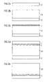
- FIG. 1 shows a cross section through the here-described component in the form of a diagrammatic sketch.
- FIGS. 2 a to 2 e illustrate the here-described method in the form of diagrammatic sketches.
- FIG. 1 shows an optoelectronic component.
- the carrier 1 can contain, for example, germanium, gallium arsenide, silicon carbide, molybdenum or another suitable material. Its thermal expansion coefficient is advantageously matched to that of the layer stack 20 , so that the heat evolved during the operation of the optoelectronic component does not place mechanical stress on the component at the interface between carrier 1 and layer stack 20 .
- carrier 1 is advantageously distinguished by good thermal conductivity. Thus the heat generated in the component can be rapidly dissipated to the environment. This increases the life of the component and enables it to be operated at higher power levels.
- Mirror layer 2 preferably contains gold or gold/germanium. It is suitable for reflecting the radiation generated in the component. Mirror layer 2 is distinguished in particular by its high reflectivity. This advantageously increases the radiation output of the component, since little or no radiation can be lost for example by absorption in carrier 1 . Mirror layer 2 is preferably vapor-deposited or sputtered on carrier 1 . Carrier 1 and mirror layer 2 are glued, soldered or bonded to layer stack 20 .
- layer stack 20 includes two active zones.
- the structure of layer stack 20 in this example is as follows: mirror layer 2 is followed by an n-cladding layer 3 , for example containing n-doped InGaP.
- n-cladding layer 3 serves to confine the charge carriers in the first active zone 4 .
- first active zone 4 which is suitable for generating electromagnetic radiation of a given first wavelength.
- Active zone 4 can contain a pn junction, a double heterostructure, a single quantum well or, particularly advantageously, a multiple quantum well structure.
- first active zone 4 contains InGaAlP.
- a first p-cladding layer 5 containing p-doped InGaAlP, for example.
- a p-contact layer 6 Applied to first p-cladding layer 5 is a p-contact layer 6 .
- Both first active zone 4 and the subsequent second active zone 8 are electrically contacted on the p-side via this p-contact layer 6 .
- the latter is advantageously transparent to the electromagnetic radiation generated in first active zone 4 and has sufficient conductivity for contacting the two active zones.
- p-contact layer 6 contains, for example, InGaAlP with an aluminum concentration of between 45% and 55%, preferably of about 50%, or AlGaAs with an aluminum concentration of between 55% and 65%, preferably 60% aluminum.
- p-contact layer 6 is exposed, for example by selective etching, to an extent such that the active zones can be contacted via this p-contact layer 6 sufficiently for the operation of the component.
- Second active zone 8 can be similar in structure to first active zone 4 and preferably generates electromagnetic radiation of a second wavelength. This second wavelength is advantageously smaller than the first wavelength, i.e., the second active zone preferably has a larger band gap than the first active zone, and the longer-wavelength electromagnetic radiation generated in first active zone 4 is therefore able to penetrate second active zone 8 without being absorbed.
- Second active zone 8 is followed by a second n-cladding layer 9 , for example containing n-doped InGaAlP.
- Layer stack 20 is terminated on its upper and lower sides by a first n-contact layer 10 and a second n-contact layer 12 , respectively.
- First n-contact layer 10 is advantageously transparent to the radiation emitted by the active zones, which is radiated in a main radiation direction 11 .
- First n-contact layer 10 can be contacted for example by means of a bonding pad placed on the surface over to one side. That is, the bonding pad is arranged for example in a corner on the upper side of n-contact layer 10 .
- a second embodiment example differs from the first solely in that layer stack 20 is constructed on the basis of an InGaAs system, i.e., the cladding layers contain suitably doped InAlGaAs and the active zones suitably doped InGaAs.
- the common p-contact layer 6 contains, for example, InAlGaAs having a suitably high aluminum concentration. It has advantageously been found in connection with this embodiment example that electromagnetic radiation in the infrared region can be radiated by the active zones.
- the described components are also suitable for producing the described components.
- suitable materials can be determined by the desired wavelengths to be emitted by the active zones.
- the layer sequence can also be modified so that the active zones are contacted by a common n-contact layer instead of a common p-contact layer.
- FIGS. 2 a to 2 e show a method of fabricating the described optoelectronic component.
- a substrate wafer 21 is first provided, as illustrated in FIG. 2 a .
- This substrate wafer can be for example a GaAs, InP or SiC wafer, depending on the material system in which the layer stack 20 is to be formed.
- Layer stack 20 including a desired number of active zones, is deposited epitaxially on substrate wafer 21 (see FIG. 2 b ).
- a mirror layer 2 is then deposited on the surface of layer stack 20 that faces substrate wafer 21 ( FIG. 2 c ). This can be done by vapor-deposition or sputtering, for example.
- Mirror layer 2 preferably contains a metal.
- FIG. 2 d shows the attachment of carrier 1 to the surface of the layer stack 20 /mirror layer 2 arrangement that faces substrate wafer 21 .
- Carrier 1 is advantageously applied by means of a solder joint, a glued joint or, particularly advantageously, a wafer bonding process.
- Substrate wafer 21 is then removed from layer stack 20 ( FIG. 2 e ).
- suitable removal methods are laser-supported processes such as laser ablation and mechanical methods such as grinding or etching.
- the arrangement is singulated, n-contact layers are applied and the common contact layers of the active zones are exposed, for example by selective etching.
- the order of these method steps can advantageously be freely selected.
Landscapes
- Led Devices (AREA)
- Photovoltaic Devices (AREA)
Applications Claiming Priority (2)
| Application Number | Priority Date | Filing Date | Title |
|---|---|---|---|
| DE102004026125.3 | 2004-05-28 | ||
| DE102004026125A DE102004026125A1 (de) | 2004-05-28 | 2004-05-28 | Optoelektronisches Bauteil und Verfahren zu dessen Herstellung |
Publications (2)
| Publication Number | Publication Date |
|---|---|
| US20050266588A1 US20050266588A1 (en) | 2005-12-01 |
| US7459727B2 true US7459727B2 (en) | 2008-12-02 |
Family
ID=34934656
Family Applications (1)
| Application Number | Title | Priority Date | Filing Date |
|---|---|---|---|
| US11/137,680 Expired - Lifetime US7459727B2 (en) | 2004-05-28 | 2005-05-25 | Optoelectronic component and method of fabricating same |
Country Status (4)
| Country | Link |
|---|---|
| US (1) | US7459727B2 (fr) |
| EP (1) | EP1601026B1 (fr) |
| JP (1) | JP2005340836A (fr) |
| DE (1) | DE102004026125A1 (fr) |
Cited By (3)
| Publication number | Priority date | Publication date | Assignee | Title |
|---|---|---|---|---|
| US20100065869A1 (en) * | 2008-09-12 | 2010-03-18 | Hitachi Cable, Ltd. | Light emitting device and method for fabricating the same |
| US20110175121A1 (en) * | 2008-01-31 | 2011-07-21 | Nikolaus Gmeinwieser | Optical-Electronic Component and Method for Production Thereof |
| US9318651B2 (en) | 2011-10-17 | 2016-04-19 | Osram Opto Semiconductors Gmbh | Optoelectronic semiconductor chip and method for producing the latter |
Families Citing this family (10)
| Publication number | Priority date | Publication date | Assignee | Title |
|---|---|---|---|---|
| DE102006039369A1 (de) | 2005-12-30 | 2007-07-05 | Osram Opto Semiconductors Gmbh | LED-Halbleiterkörper und Verwendung eines LED-Halbleiterkörpers |
| DE102006035627A1 (de) | 2006-07-31 | 2008-02-07 | Osram Opto Semiconductors Gmbh | LED-Halbleiterkörper |
| DE102006051745B4 (de) * | 2006-09-28 | 2024-02-08 | OSRAM Opto Semiconductors Gesellschaft mit beschränkter Haftung | LED-Halbleiterkörper und Verwendung eines LED-Halbleiterkörpers |
| JP2008159629A (ja) * | 2006-12-20 | 2008-07-10 | Rohm Co Ltd | 光通信用半導体素子 |
| JP2008159628A (ja) * | 2006-12-20 | 2008-07-10 | Rohm Co Ltd | 半導体発光素子及び半導体発光素子の製造方法 |
| DE102008014094A1 (de) | 2008-03-13 | 2009-09-17 | Osram Opto Semiconductors Gmbh | Strahlungsemittierende Vorrichtung und Verfahren zur Herstellung einer strahlungsemittierenden Vorrichtung |
| DE102008021620A1 (de) | 2008-04-30 | 2009-11-05 | Osram Opto Semiconductors Gmbh | Strahlung emittierender Dünnfilm-Halbleiterchip und Verfahren zur Herstellung eines Strahlung emittierenden Dünnfilm-Halbleiterchips |
| DE102008050643B4 (de) | 2008-10-07 | 2022-11-03 | OSRAM Opto Semiconductors Gesellschaft mit beschränkter Haftung | Leuchtmittel |
| JP5755511B2 (ja) * | 2011-06-14 | 2015-07-29 | Dowaエレクトロニクス株式会社 | 半導体発光素子およびその製造方法 |
| CN104617122A (zh) * | 2015-01-07 | 2015-05-13 | 中国科学院半导体研究所 | 单芯片多电极调控多波长发光二极管结构及制备方法 |
Citations (12)
| Publication number | Priority date | Publication date | Assignee | Title |
|---|---|---|---|---|
| US5391896A (en) | 1992-09-02 | 1995-02-21 | Midwest Research Institute | Monolithic multi-color light emission/detection device |
| US5684309A (en) | 1996-07-11 | 1997-11-04 | North Carolina State University | Stacked quantum well aluminum indium gallium nitride light emitting diodes |
| US5699375A (en) * | 1996-07-08 | 1997-12-16 | Xerox Corporation | Multiple wavelength, surface emitting laser with broad bandwidth distributed Bragg reflectors |
| WO1998031055A1 (fr) | 1997-01-09 | 1998-07-16 | Nichia Chemical Industries, Ltd. | Dispositif a semi-conducteur au nitrure |
| US5831277A (en) | 1997-03-19 | 1998-11-03 | Northwestern University | III-nitride superlattice structures |
| DE19819543A1 (de) | 1998-04-30 | 1999-11-11 | Siemens Ag | Lichtemissions-Halbleitereinrichtung |
| WO2001039282A2 (fr) | 1999-11-19 | 2001-05-31 | Osram Opto Semiconductors Gmbh & Co. Ohg | Dispositif a semiconducteur optique dote d'une structure de puits quantique multicouche |
| DE10026255A1 (de) | 2000-04-26 | 2001-11-08 | Osram Opto Semiconductors Gmbh | Lumineszenzdiosdenchip auf der Basis von GaN und Verfahren zum Herstellen eines Lumineszenzdiodenbauelements mit einem Lumineszenzdiodenchip auf der Basis von GaN |
| US6487230B1 (en) * | 1998-04-14 | 2002-11-26 | Bandwidth 9, Inc | Vertical cavity apparatus with tunnel junction |
| US6563139B2 (en) | 2001-09-11 | 2003-05-13 | Chang Hsiu Hen | Package structure of full color LED form by overlap cascaded die bonding |
| JP2003152222A (ja) | 2001-11-14 | 2003-05-23 | Lecip Corp | 多色半導体発光素子及びその製造方法 |
| US6806112B1 (en) * | 2003-09-22 | 2004-10-19 | National Chung-Hsing University | High brightness light emitting diode |
Family Cites Families (13)
| Publication number | Priority date | Publication date | Assignee | Title |
|---|---|---|---|---|
| JPH05251739A (ja) * | 1992-03-06 | 1993-09-28 | Toshiba Corp | 半導体発光デバイス |
| US5376580A (en) * | 1993-03-19 | 1994-12-27 | Hewlett-Packard Company | Wafer bonding of light emitting diode layers |
| FR2726126A1 (fr) * | 1994-10-24 | 1996-04-26 | Mitsubishi Electric Corp | Procede de fabrication de dispositifs a diodes electroluminescentes a lumiere visible |
| JP3409958B2 (ja) * | 1995-12-15 | 2003-05-26 | 株式会社東芝 | 半導体発光素子 |
| JPH09232627A (ja) * | 1996-02-26 | 1997-09-05 | Matsushita Electric Ind Co Ltd | 白色発光素子 |
| JP3643225B2 (ja) * | 1997-12-03 | 2005-04-27 | ローム株式会社 | 光半導体チップ |
| US6841805B2 (en) | 1999-10-08 | 2005-01-11 | Mccann & Associates, Inc. | Method for generating mid-infrared light |
| JP3486900B2 (ja) * | 2000-02-15 | 2004-01-13 | ソニー株式会社 | 発光装置およびそれを用いた光装置 |
| TW497277B (en) | 2000-03-10 | 2002-08-01 | Toshiba Corp | Semiconductor light emitting device and method for manufacturing the same |
| JP3940596B2 (ja) * | 2001-05-24 | 2007-07-04 | 松下電器産業株式会社 | 照明光源 |
| US6759689B2 (en) * | 2002-08-07 | 2004-07-06 | Shin-Etsu Handotai Co., Ltd. | Light emitting element and method for manufacturing the same |
| US6822991B2 (en) * | 2002-09-30 | 2004-11-23 | Lumileds Lighting U.S., Llc | Light emitting devices including tunnel junctions |
| JP2004327719A (ja) * | 2003-04-24 | 2004-11-18 | Shin Etsu Handotai Co Ltd | 発光素子 |
-
2004
- 2004-05-28 DE DE102004026125A patent/DE102004026125A1/de not_active Ceased
-
2005
- 2005-03-31 EP EP05007104.2A patent/EP1601026B1/fr not_active Expired - Lifetime
- 2005-05-25 US US11/137,680 patent/US7459727B2/en not_active Expired - Lifetime
- 2005-05-27 JP JP2005156347A patent/JP2005340836A/ja active Pending
Patent Citations (15)
| Publication number | Priority date | Publication date | Assignee | Title |
|---|---|---|---|---|
| US5391896A (en) | 1992-09-02 | 1995-02-21 | Midwest Research Institute | Monolithic multi-color light emission/detection device |
| US5699375A (en) * | 1996-07-08 | 1997-12-16 | Xerox Corporation | Multiple wavelength, surface emitting laser with broad bandwidth distributed Bragg reflectors |
| US5684309A (en) | 1996-07-11 | 1997-11-04 | North Carolina State University | Stacked quantum well aluminum indium gallium nitride light emitting diodes |
| US6172382B1 (en) | 1997-01-09 | 2001-01-09 | Nichia Chemical Industries, Ltd. | Nitride semiconductor light-emitting and light-receiving devices |
| WO1998031055A1 (fr) | 1997-01-09 | 1998-07-16 | Nichia Chemical Industries, Ltd. | Dispositif a semi-conducteur au nitrure |
| EP1017113A1 (fr) | 1997-01-09 | 2000-07-05 | Nichia Chemical Industries, Ltd. | Dispositif a semi-conducteur au nitrure |
| US5831277A (en) | 1997-03-19 | 1998-11-03 | Northwestern University | III-nitride superlattice structures |
| US6487230B1 (en) * | 1998-04-14 | 2002-11-26 | Bandwidth 9, Inc | Vertical cavity apparatus with tunnel junction |
| WO1999057788A2 (fr) | 1998-04-30 | 1999-11-11 | Osram Opto Semiconductors Gmbh & Co. Ohg | Dispositif semi-conducteur a emission de lumiere |
| DE19819543A1 (de) | 1998-04-30 | 1999-11-11 | Siemens Ag | Lichtemissions-Halbleitereinrichtung |
| WO2001039282A2 (fr) | 1999-11-19 | 2001-05-31 | Osram Opto Semiconductors Gmbh & Co. Ohg | Dispositif a semiconducteur optique dote d'une structure de puits quantique multicouche |
| DE10026255A1 (de) | 2000-04-26 | 2001-11-08 | Osram Opto Semiconductors Gmbh | Lumineszenzdiosdenchip auf der Basis von GaN und Verfahren zum Herstellen eines Lumineszenzdiodenbauelements mit einem Lumineszenzdiodenchip auf der Basis von GaN |
| US6563139B2 (en) | 2001-09-11 | 2003-05-13 | Chang Hsiu Hen | Package structure of full color LED form by overlap cascaded die bonding |
| JP2003152222A (ja) | 2001-11-14 | 2003-05-23 | Lecip Corp | 多色半導体発光素子及びその製造方法 |
| US6806112B1 (en) * | 2003-09-22 | 2004-10-19 | National Chung-Hsing University | High brightness light emitting diode |
Non-Patent Citations (1)
| Title |
|---|
| Schnitzer et al., "30% external quantum efficiency from surface textured, thin-film light-emitting diodes" Appl. Phys. Lett., vol. 63, No. 16, pp. 2174-2176 (Oct. 18, 1993). |
Cited By (5)
| Publication number | Priority date | Publication date | Assignee | Title |
|---|---|---|---|---|
| US20110175121A1 (en) * | 2008-01-31 | 2011-07-21 | Nikolaus Gmeinwieser | Optical-Electronic Component and Method for Production Thereof |
| US8686451B2 (en) | 2008-01-31 | 2014-04-01 | Osram Opto Semiconductor Gmbh | Optical-electronic component and method for production thereof |
| US20100065869A1 (en) * | 2008-09-12 | 2010-03-18 | Hitachi Cable, Ltd. | Light emitting device and method for fabricating the same |
| US7884381B2 (en) * | 2008-09-12 | 2011-02-08 | Hitachi Cable, Ltd. | Light emitting device and method for fabricating the same including a back surface electrode with an Au alloy |
| US9318651B2 (en) | 2011-10-17 | 2016-04-19 | Osram Opto Semiconductors Gmbh | Optoelectronic semiconductor chip and method for producing the latter |
Also Published As
| Publication number | Publication date |
|---|---|
| DE102004026125A1 (de) | 2005-12-22 |
| EP1601026B1 (fr) | 2018-11-28 |
| EP1601026A2 (fr) | 2005-11-30 |
| EP1601026A3 (fr) | 2010-11-10 |
| US20050266588A1 (en) | 2005-12-01 |
| JP2005340836A (ja) | 2005-12-08 |
Similar Documents
| Publication | Publication Date | Title |
|---|---|---|
| KR100984921B1 (ko) | 평면형 전방향성 반사기를 가진 발광 다이오드 | |
| US7319247B2 (en) | Light emitting-diode chip and a method for producing same | |
| US6492661B1 (en) | Light emitting semiconductor device having reflection layer structure | |
| EP1072072B1 (fr) | Dispositif optique à l'émission par la surface | |
| US6825502B2 (en) | Light emitting element, method of manufacturing the same, and semiconductor device having light emitting element | |
| US5793062A (en) | Transparent substrate light emitting diodes with directed light output | |
| US8093607B2 (en) | Optoelectronic semiconductor component | |
| US6015719A (en) | Transparent substrate light emitting diodes with directed light output | |
| US20090140279A1 (en) | Substrate-free light emitting diode chip | |
| US20030231683A1 (en) | Nitride based semiconductor structures with highly reflective mirrors | |
| US7019330B2 (en) | Resonant cavity light emitting device | |
| US7459727B2 (en) | Optoelectronic component and method of fabricating same | |
| KR20080087135A (ko) | 질화물 반도체 발광 소자 | |
| JP2001144321A (ja) | 発光素子及びその製造方法 | |
| US7375377B2 (en) | Ingan-based light-emitting diode chip and a method for the production thereof | |
| WO2014042198A1 (fr) | Diode électroluminescente et procédé permettant de produire cette dernière | |
| US20220021185A1 (en) | Optoelectronic semiconductor component having a current distribution layer and method for producing the optoelectronic semiconductor component | |
| JP2006013381A (ja) | 発光素子 | |
| JP2012129249A (ja) | 発光ダイオード、発光ダイオードランプ及び発光ダイオードの製造方法 | |
| JP2004304048A (ja) | 発光ダイオード用エピタキシャルウエハ |
Legal Events
| Date | Code | Title | Description |
|---|---|---|---|
| AS | Assignment |
Owner name: OSRAM OPTO SEMICONDUCTORS GMBH, GERMANY Free format text: ASSIGNMENT OF ASSIGNORS INTEREST;ASSIGNOR:STAUSS, PETER;REEL/FRAME:016573/0372 Effective date: 20050712 |
|
| STCF | Information on status: patent grant |
Free format text: PATENTED CASE |
|
| FEPP | Fee payment procedure |
Free format text: PAYOR NUMBER ASSIGNED (ORIGINAL EVENT CODE: ASPN); ENTITY STATUS OF PATENT OWNER: LARGE ENTITY |
|
| FPAY | Fee payment |
Year of fee payment: 4 |
|
| FPAY | Fee payment |
Year of fee payment: 8 |
|
| AS | Assignment |
Owner name: OSRAM OLED GMBH, GERMANY Free format text: ASSIGNMENT OF ASSIGNORS INTEREST;ASSIGNOR:OSRAM OPTO SEMICONDUCTORS GMBH;REEL/FRAME:051467/0906 Effective date: 20191218 |
|
| MAFP | Maintenance fee payment |
Free format text: PAYMENT OF MAINTENANCE FEE, 12TH YEAR, LARGE ENTITY (ORIGINAL EVENT CODE: M1553); ENTITY STATUS OF PATENT OWNER: LARGE ENTITY Year of fee payment: 12 |