US7518149B2 - Light emitting mesa structures with high aspect ratio and near-parabolic sidewalls - Google Patents
Light emitting mesa structures with high aspect ratio and near-parabolic sidewalls Download PDFInfo
- Publication number
- US7518149B2 US7518149B2 US11/264,341 US26434105A US7518149B2 US 7518149 B2 US7518149 B2 US 7518149B2 US 26434105 A US26434105 A US 26434105A US 7518149 B2 US7518149 B2 US 7518149B2
- Authority
- US
- United States
- Prior art keywords
- mesa
- optical device
- active layer
- light
- semiconductor
- Prior art date
- Legal status (The legal status is an assumption and is not a legal conclusion. Google has not performed a legal analysis and makes no representation as to the accuracy of the status listed.)
- Expired - Lifetime, expires
Links
Images




Classifications
-
- H—ELECTRICITY
- H10—SEMICONDUCTOR DEVICES; ELECTRIC SOLID-STATE DEVICES NOT OTHERWISE PROVIDED FOR
- H10H—INORGANIC LIGHT-EMITTING SEMICONDUCTOR DEVICES HAVING POTENTIAL BARRIERS
- H10H20/00—Individual inorganic light-emitting semiconductor devices having potential barriers, e.g. light-emitting diodes [LED]
- H10H20/80—Constructional details
- H10H20/81—Bodies
- H10H20/819—Bodies characterised by their shape, e.g. curved or truncated substrates
-
- H—ELECTRICITY
- H10—SEMICONDUCTOR DEVICES; ELECTRIC SOLID-STATE DEVICES NOT OTHERWISE PROVIDED FOR
- H10F—INORGANIC SEMICONDUCTOR DEVICES SENSITIVE TO INFRARED RADIATION, LIGHT, ELECTROMAGNETIC RADIATION OF SHORTER WAVELENGTH OR CORPUSCULAR RADIATION
- H10F77/00—Constructional details of devices covered by this subclass
- H10F77/10—Semiconductor bodies
- H10F77/14—Shape of semiconductor bodies; Shapes, relative sizes or dispositions of semiconductor regions within semiconductor bodies
- H10F77/147—Shapes of bodies
-
- H—ELECTRICITY
- H10—SEMICONDUCTOR DEVICES; ELECTRIC SOLID-STATE DEVICES NOT OTHERWISE PROVIDED FOR
- H10H—INORGANIC LIGHT-EMITTING SEMICONDUCTOR DEVICES HAVING POTENTIAL BARRIERS
- H10H20/00—Individual inorganic light-emitting semiconductor devices having potential barriers, e.g. light-emitting diodes [LED]
- H10H20/80—Constructional details
- H10H20/81—Bodies
- H10H20/813—Bodies having a plurality of light-emitting regions, e.g. multi-junction LEDs or light-emitting devices having photoluminescent regions within the bodies
-
- H—ELECTRICITY
- H10—SEMICONDUCTOR DEVICES; ELECTRIC SOLID-STATE DEVICES NOT OTHERWISE PROVIDED FOR
- H10H—INORGANIC LIGHT-EMITTING SEMICONDUCTOR DEVICES HAVING POTENTIAL BARRIERS
- H10H20/00—Individual inorganic light-emitting semiconductor devices having potential barriers, e.g. light-emitting diodes [LED]
- H10H20/80—Constructional details
- H10H20/81—Bodies
- H10H20/819—Bodies characterised by their shape, e.g. curved or truncated substrates
- H10H20/821—Bodies characterised by their shape, e.g. curved or truncated substrates of the light-emitting regions, e.g. non-planar junctions
-
- Y—GENERAL TAGGING OF NEW TECHNOLOGICAL DEVELOPMENTS; GENERAL TAGGING OF CROSS-SECTIONAL TECHNOLOGIES SPANNING OVER SEVERAL SECTIONS OF THE IPC; TECHNICAL SUBJECTS COVERED BY FORMER USPC CROSS-REFERENCE ART COLLECTIONS [XRACs] AND DIGESTS
- Y02—TECHNOLOGIES OR APPLICATIONS FOR MITIGATION OR ADAPTATION AGAINST CLIMATE CHANGE
- Y02E—REDUCTION OF GREENHOUSE GAS [GHG] EMISSIONS, RELATED TO ENERGY GENERATION, TRANSMISSION OR DISTRIBUTION
- Y02E10/00—Energy generation through renewable energy sources
- Y02E10/50—Photovoltaic [PV] energy
Definitions
- the invention relates to light emitting diodes (LEDs) and photodiodes (PDs).
- LEDs convert electrical energy into optical energy
- PDs convert optical energy into electrical energy.
- light is usually generated through recombination of electrons, originating from an n-type doped semiconductor layer, and holes originating from a p-type doped semiconductor layer.
- light can be generated by electron intersub-band transitions rather than electron hole transitions.
- LEL light-emitting layer
- a major challenge is to extract as much of the emitted light as possible from the semiconductor material into the surrounding medium, usually air. This is hindered by total internal reflection at the surfaces of the semiconductor.
- the average path length for light rays within the semiconductor is long, and the average number of reflections of an emitted light ray at semiconductor surfaces is high, prior to escape.
- Long path lengths and reflections at metal coated semiconductor surfaces both lead to absorption losses.
- the light that does escape, escapes to a large extent through the sides of the chip and an external mirror is needed to collect this light into a useful light beam.
- Another approach is called chip shaping. Higher extraction efficiencies (EEs) are possible with this approach.
- EEs extraction efficiencies
- it does not eliminate the long path lengths within the semiconductor chip, nor the requirement for an external mirror.
- the technique is less suitable to the widely used gallium nitride (GaN) based materials systems.
- an optical device comprising a semiconductor diode having an active layer enclosed in a semiconductor structure mesa, in which:
- the mesa cross sectional area (A c ) at the level of the active layer is less than 100 ⁇ m 2 ;
- the mesa has an aspect ratio ((H 3 ) ⁇ (H 3 )/A c ) greater than 3.
- the mesa has an aspect ratio ((H 3 ) ⁇ (H 3 )/A c ) greater than 8.
- the mesa further comprises an electrical contact on the truncated top.
- the electrical contact occupies less than 16% of the area of the truncated top.
- the mesa side walls are curved, the side wall angle ⁇ increasing continuously from the active layer towards the transmitting or receiving face.
- the cross sectional area (A c ) of the mesa is rectangular in shape, the length being more than twice the width.
- the active layer is of InGaN material.
- the active layer is of InGaAs material.
- the active layer is of InGaAsP material.
- the active layer is of ZnCdSeTe material.
- the height (H 3 ) of the mesa is greater than 5 ⁇ m.
- the active layer is an emitting layer whereby the device is an LED.
- the active layer is a detecting layer, whereby the device is a photodiode.
- the device comprises an array of diodes.
- the array comprises conductors so that individual diodes or diode clusters are individually addressable, thus forming an addressable LED or PD array.
- the device area covered with diode mesas is greater than 10 mm 2 , and wherein more than 80% of all extracted light is extracted through a back surface, whereby the device is scalable and suitable for high light outputs from a single array-chip.
- the area covered with diode mesas is greater than 100 mm 2 .
- the array is configured as a flip-clip, mounted on a heat sink.
- the invention also provides a method of fabricating a diode array as defined above, wherein a single lithography step is followed by the following three processing steps, without additional lithography:
- the etch mask for the semiconductor mesa etch comprises a multi-layer of more than one layer, and one or more layers are etched selectively after the mesa etch step to create an overhang profile, suitable for pattern definition through lift-off of a subsequent coating.
- the etch mask is re-flowed prior to etching to provide a desired sidewall profile for the semiconductor mesa.
- the multi-layer etch mask consists of a double-level resist.
- the method comprises an additional oxygen plasma step to reduce the D 1 /D 2 ratio.
- the electrical contact and the flip-chip bonding metallisation are all deposited in one step, without additional lithography.
- FIG. 1 is a diagrammatic cross sectional view of a single element of a micro LED array device
- FIG. 2 is a plan view
- FIG. 3 is a plan view of an alternative device
- FIG. 4 defines the angle ⁇ between the light emitting layer (LEL) and the mesa sidewall
- FIG. 5 is a plot of extraction efficiency into air versus aspect ratio (H 4 /D 4 ) for paraboloid shaped reflectors in semiconductor material with a refractive index of 2.28;
- FIG. 6 shows the effect of the top electrical contact reflectivity on the results obtained in FIG. 5 ;
- FIG. 7 is a plot showing the effect of the light emitting layer position with respect to the focal plane of the paraboloid (the focal plane being defined as the horizontal plane that intersects the focal point of the paraboloid);
- FIG. 8 is a set of beam profiles for a Lambertian emitter and for two parabolic micro-LEDs with different aspect ratios (other parameters the same as in FIG. 5 );
- FIG. 9 is a photograph of micro-LEDs, fabricated on GaN/sapphire material.
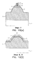
- FIGS. 10( a ) to 10 ( h ) are a sequence of diagrams showing steps of a production process for producing a device of the invention, FIGS. 10( g ) and 10 ( h ) showing a diagram of a cluster of micro-LEDs both in cross-section and in plan view;
- FIG. 11 is a photograph showing light emission from a cluster of fabricated micro-LEDs on GaN/sapphire, as observed through the transparent sapphire substrate;
- FIG. 12 is a plot of emitted intensity versus position for a single LED element (near field).
- FIG. 13 is a plot of light intensity versus position, on a line across a single micro-LED element, as shown in FIG. 12 .
- the invention provides an optical device consisting of one or an array of highly efficient micro-LEDs, and a manufacturing process.
- Each micro-LED is an integrated diode structure in a mesa shape, in which the mesa shape and the light-emitting region are chosen for optimum efficiency.
- the following description refers to a device having an array of elements, and the elements are light emitting diodes rather than photodiodes.
- a single one of the micro-LEDs 100 comprises, on a substrate 101 and a semiconductor layer 102 , a mesa 103 , a light emitting layer 104 , and an electrical contact 106 .
- the micro-LEDs in this device have a very high EE because of their shape. Light is generated within the mesa, which is shaped to enhance the escape probability of the light. Very high EEs are achieved, particularly with a near-parabolic mesa that has a high aspect ratio.
- the top of the mesa is truncated above the light-emitting layer (LEL), providing a flat surface for the electrical contact 106 on the top of the semiconductor mesa.
- LEL light-emitting layer
- the EE is high provided the top contact has a good reflectivity value. Also, it has been found that efficiency is particularly high if the contact 106 occupies an area of less than 16% of the truncated top mesa surface area. This feature also helps to achieve a more directional beam in the case of the device being an LED.
- Having a high aspect ratio is effective, as is clear from FIGS. 5 and 6 . It is preferably greater than 0.5, and more preferably greater than 3, and most preferably greater than 8.
- the aspect ratio is calculated variously based on H 3 /D 4 , H 4 /D 4 , and ((H 3 ) ⁇ (H 3 )/A c ). The former two are used for modelling purposes, and the latter as a measurable one based on measurable dimensions in the physical device. In fact, all three definitions yield very similar results.
- the light is generated in GaN based micro-LEDs, and the light is efficiently emitted through a sapphire substrate.
- the shape of the micro-LEDs also allows the light from each micro-LED to be very directional, which is an advantage in many applications, such as light coupling to fibres or waveguides. While in this example visible light emission was used, the invention holds also for LEDs emitting in the invisible part of the spectrum, i.e. in the ultra-violet or infrared. And while in this example a transparent sapphire substrate was used, the invention would remain valid if there were no separate substrate present.
- a micro-LED 1 of the array comprises regions as follows:
- each micro-LED may be “stretched” in one direction, as shown in FIG. 3 , depending on the application.
- a device 120 has a semiconductor layer 122 , a mesa 123 , a light emitting layer 124 , and a contact 126 .
- the array has the following properties:
- FIG. 4 is a diagram defining the angle ⁇ between the LEL and the mesa sidewall.
- FIG. 5 shows the calculated extraction efficiency as a function of the aspect ratio H 4 /D 4 of a paraboloid shaped device. For high aspect ratios, and high top contact reflectivities, the calculated extraction efficiency approaches 100%. This is much higher than on most presently available commercial LEDs. The best commercial GaN based LEDs have extraction efficiencies of about 45%.
- D 1 D 2
- H 1 H 2
- D 3 /D 2 1.12
- R 100% at the top electrical contact.
- all reflections from the side surfaces were assumed to be 100% reflective and the rays that hit the bottom semiconductor to air interface within the critical angle were 100% transmitted, while rays hitting this interface outside the critical angle were considered as lost.
- FIG. 5 also shows the portion of light emerging into air that is confined to a 30° cone (for the same paraboloids).
- FIG. 6 Extraction efficiency values as a function of top electrical contact reflectivity are shown in FIG. 6 .
- FIG. 7 shows the effect of the location of the LEL with respect to the focal plane of the paraboloid on the efficiency. This shows that the devices remain effective even when the LEL is slightly offset with respect to the focal plane.
- FIG. 8 compares the beam properties from paraboloid micro-LEDs with the Lambertian beam properties of standard cuboid shaped chips. In the calculations above, Fresnel losses (due to partial reflection) at the interfaces have been ignored. Such losses can be kept at a minimum by coating the bottom surface with an anti-reflection coating.
- FIG. 9 A photograph of some fabricated micro-LEDs is shown in FIG. 9 .
- micro-LEDs allow potentially almost 100% light extraction, provided that the semiconductor material and the (optional) substrate are transparent at the emission wavelength of the LED.
- a higher light extraction efficiency means less heat dissipation, which in turn allows for a higher operating current, thus further increasing the possible light output from a single device.
- This will become an important feature once the internal quantum efficiency in a material comes close to 100%, as the light output starts then to rise much faster than linearly with EE.
- An important feature of each micro-LED is that, because of the shape of the mesa, there is nearly total internal reflection from the mesa walls, causing almost all light to exit at the bottom. This has been achieved without need for fabricating a reflector around the mesa, the internal reflection being achieved because of the shape.
- the invention also allows for large single chip dimensions, without sacrificing extraction efficiency.
- light extraction through the sides of the chip becomes less effective when the chip area is increased. This limits practical GaN/sapphire chip areas to about 2 mm ⁇ 2 mm.
- a 60-Watt incandescent bulb emits about 1,000 lumens.
- a car headlight requires about 1,800 lumens.
- the present invention may provide these light output levels with a single GaN based LED chip.
- the light rays generally have a short trajectory within the semiconductor, thus minimising absorption.
- the reflections of rays incident on the parabolic sidewalls are mainly at angles greater than the critical angle and therefore virtually loss-less.
- the majority of the rays that hit the top electrical contact hit it only once.
- the emerging light beam can be highly directional (see FIG. 8 ).
- the directional nature of the beam is useful for coupling light into a plastic optical fibre (POF) for example in data communications applications. Coupling of light from an LED into a multi mode fibre may also become a practical possibility.
- the directionality can be enhanced by increasing the H 4 /D 4 ratio (see FIG. 7 ), and further increased by decreasing the D 1 /D 2 ratio.
- the fabrication process can be used to control both these ratios.
- each individual LED element is highly contained, and very little light spreads sideways. This is good for micro-LED displays where light ought to emerge from only one pixel and should not spread to neighbouring pixels.
- the arrangement is compatible with flip-chip bonding techniques, which themselves allow for higher operating currents through improved heat sinking.
- the parabolic emitters will allow higher light-outputs from a single LED.
- the design and fabrication technique are suitable for all semiconductor materials systems where the light can be extracted through a transparent bottom.
- Examples of such systems are: GaN/sapphire, GaN/SiC, InGaAs/GaAs, and InGaAsP/InP.
- the invention applies to either p-type doped semiconductor above the LEL, and n-type doped semiconductor below the LEL, or with n-type doped semiconductor above the LEL, and p-type doped semiconductor below the LEL.
- FIGS. 10( a ) to 10 ( h ) the fabrication of the micro-LEDs is now described.
- the labels used are:
- Steps 1 , 2 ( FIG. 10( a )): Perform lithography on a dual layer resist.
- the bottom layer is pre-exposed, and can be further developed later on in the process.
- the bottom layer can also be another sacrificial layer that can be etched later on to create an undercut profile for selective lift-off of part of the insulating layer.
- Step 3 ( FIG. 10( b )): The multi-layer is reflowed to the desired shape at a specific time and temperature, to create in the next step a near-parabolic profile in the semiconductor.
- Step 4 ( FIG. 10( c )): Dry etching, e.g. by ICP or RIE to transfer the desired shape into the semiconductor.
- Step 5 ( FIG. 10( d )) (Optional): An oxygen plasma step to reduce the size of the multi-layer mound. This will allow for a top electrical contact that is smaller than the top diameter of the mesa, i.e. (D 1 /D 2 ) ⁇ 1.
- Step 6 ( FIG. 10( d )): Further develop the bottom layer to create an overhang profile in the two-layer resist. This is to facilitate the lift-off of part of the insulating coating, to make place for the top electrical contact.
- Step 7 ( FIG. 10( e )): An insulating coating is deposited over the mesas.
- Step 8 ( FIG. 10( f )): The remaining resist and the unwanted insulator coating are removed. This is being facilitated by the resist undercut generated in step 6 .
- Step 9 An electrical contact layer is deposited over the entire insulator coating. At the centre of each mesa this layer makes contact with the semiconductor, providing the electrical contact to the top of the semiconductor mesas.
- Step 10 Bottom contact deposition and patterning. This provides the electrical contacts to the semiconductor bottom.
- the top contact can be either to p-type or to n-type semiconductor.
- FIG. 11 is a photograph showing light emission from a cluster of fabricated micro-LEDs on GaN, as observed through the transparent sapphire substrate (near field). It shows the clear contribution to the light output from the near parabolic side surfaces.
- FIG. 12 is a plot of emitted intensity versus position for a single such LED element.
- FIG. 13 shows the intensity as a function of position on a line that intersects the centre of the micro-LED element.
- the H 3 /D 3 ratio for the elements shown in FIGS. 11-13 is approximately 0.5.
- the wafer was sapphire/n-GaN/InGaN multiple quantum well region/p-GaN.
- the top contact was Ni/Au.
- the insulating coating was evaporated SiO 2 .
- the bottom contact was Ti/Al.
- the EE through the bottom surface increased by about a factor 3 on these devices, due to the surface shaping.
- the invention provides an LED chip with improved EE and directionality, and a simple and effective fabrication method.
- the active layer could be of any semiconductor material of type IV (e.g. Si, Ge, SiGe), type III-V (e.g. InGaAs, InGaAsP, InGaN, AlInGaN), or type II-IV material (e.g. ZnO, ZnCdSeTe).
- the light in the active layer may be generated by inter-sub-band transitions.
- the active layer may be of quantum dot material.
- the active layer may contain Sb.
- the device may be a photodiode or a photodiode array, in which the active layer detects light.
Landscapes
- Led Devices (AREA)
- Optical Elements Other Than Lenses (AREA)
Applications Claiming Priority (3)
| Application Number | Priority Date | Filing Date | Title |
|---|---|---|---|
| IE2003/0332 | 2003-05-02 | ||
| IE20030332 | 2003-05-02 | ||
| PCT/IE2004/000063 WO2004097947A2 (fr) | 2003-05-02 | 2004-05-04 | Diodes electroluminescentes et leur procede de fabrication |
Related Parent Applications (1)
| Application Number | Title | Priority Date | Filing Date |
|---|---|---|---|
| PCT/IE2004/000063 Continuation WO2004097947A2 (fr) | 2003-05-02 | 2004-05-04 | Diodes electroluminescentes et leur procede de fabrication |
Publications (2)
| Publication Number | Publication Date |
|---|---|
| US20060113638A1 US20060113638A1 (en) | 2006-06-01 |
| US7518149B2 true US7518149B2 (en) | 2009-04-14 |
Family
ID=33397630
Family Applications (1)
| Application Number | Title | Priority Date | Filing Date |
|---|---|---|---|
| US11/264,341 Expired - Lifetime US7518149B2 (en) | 2003-05-02 | 2005-10-28 | Light emitting mesa structures with high aspect ratio and near-parabolic sidewalls |
Country Status (7)
| Country | Link |
|---|---|
| US (1) | US7518149B2 (fr) |
| EP (1) | EP1620902B1 (fr) |
| JP (1) | JP2006525669A (fr) |
| AT (1) | ATE474332T1 (fr) |
| DE (1) | DE602004028115D1 (fr) |
| IE (1) | IE20040308A1 (fr) |
| WO (1) | WO2004097947A2 (fr) |
Cited By (50)
| Publication number | Priority date | Publication date | Assignee | Title |
|---|---|---|---|---|
| WO2013117760A1 (fr) | 2012-02-10 | 2013-08-15 | University College Cork, National University Of Ireland, Cork | Puce de diode électroluminescente |
| WO2013117944A1 (fr) | 2012-02-09 | 2013-08-15 | Mled Limited | Extraction améliorée de la lumière |
| WO2013121051A1 (fr) * | 2012-02-16 | 2013-08-22 | University College Cork, National University Of Ireland, Cork | Micro-réseau de diodes électroluminescentes (del) avec des filtres |
| WO2014032997A1 (fr) | 2012-09-03 | 2014-03-06 | Infiniled Limited | Dispositif optique |
| DE102012217967A1 (de) | 2012-10-01 | 2014-04-03 | Carl Zeiss Microscopy Gmbh | Konfokales Mikroskop mit frei einstellbarer Probenabtastung |
| US9480399B2 (en) | 2014-06-26 | 2016-11-01 | Carl Zeiss Meditec Ag | Illumination device for an optical viewing apparatus |
| US20170076693A1 (en) * | 2014-02-19 | 2017-03-16 | PA. COTTE Family Holding GmbH | Display device with better contrast |
| WO2017083731A1 (fr) | 2015-11-13 | 2017-05-18 | Oculus Vr, Llc | Procédé et appareil destinés à être utilisés dans la fabrication d'un élément d'affichage |
| WO2017175148A1 (fr) | 2016-04-08 | 2017-10-12 | Novagan | Source de lumière hautement directionnelle à rendement d'extraction élevé, et procédé de fabrication de cette source de lumière |
| US10020422B1 (en) | 2017-09-29 | 2018-07-10 | Oculus Vr, Llc | Mesa shaped micro light emitting diode with bottom N-contact |
| WO2018200417A1 (fr) | 2017-04-24 | 2018-11-01 | Pcms Holdings, Inc. | Systèmes et procédés destinés à des affichages 3d à couches optiques flexibles |
| WO2019040484A1 (fr) | 2017-08-23 | 2019-02-28 | Pcms Holdings, Inc. | Procédé et appareil pour générer des champs lumineux projetés en 3d à l'aide de moteur de projection d'image à champs lumineux |
| US10262977B2 (en) | 2014-07-31 | 2019-04-16 | Facebook Technologies, Llc | Colour inorganic LED display for display devices with a high number of pixel |
| US10325791B1 (en) | 2017-12-13 | 2019-06-18 | Facebook Technologies, Llc | Formation of elastomeric layer on selective regions of light emitting device |
| US10326052B1 (en) * | 2018-02-12 | 2019-06-18 | Facebook Technologies, Llc | Light emitting diode with field enhanced contact |
| US10418510B1 (en) | 2017-12-22 | 2019-09-17 | Facebook Technologies, Llc | Mesa shaped micro light emitting diode with electroless plated N-contact |
| US20190305188A1 (en) * | 2018-03-30 | 2019-10-03 | Facebook Technologies, Llc | Reduction of surface recombination losses in micro-leds |
| US10468552B2 (en) | 2018-03-30 | 2019-11-05 | Facebook Technologies, Llc | High-efficiency micro-LEDs |
| WO2019221993A1 (fr) | 2018-05-17 | 2019-11-21 | Pcms Holdings, Inc. | Rétroéclairage directionnel d'affichage en 3d basé sur des éléments de diffraction |
| US10490699B2 (en) * | 2014-11-24 | 2019-11-26 | Facebook Technologies, Llc | Micro-LED device |
| US10490599B2 (en) | 2017-07-13 | 2019-11-26 | Applied Materials, Inc. | Collimated, directional micro-LED light field display |
| US10515580B2 (en) | 2014-07-31 | 2019-12-24 | Facebook Technologies, Llc | Colour ILED display on silicon |
| WO2020008200A1 (fr) | 2018-07-06 | 2020-01-09 | Plessey Semiconductors Limited | Réseau de del monolithique et précurseur associé |
| US10559730B2 (en) | 2016-12-09 | 2020-02-11 | Applied Materials, Inc. | Collimated LED light field display |
| US10574354B2 (en) * | 2017-12-12 | 2020-02-25 | International Business Machines Corporation | Data transfer arrangement for a hybrid integrated circuit (HIC) and an HIC with the data transfer arrangement |
| US10593854B1 (en) | 2006-12-11 | 2020-03-17 | The Regents Of The University Of California | Transparent light emitting device with light emitting diodes |
| US10622519B2 (en) | 2018-03-30 | 2020-04-14 | Facebook Technologies, Llc | Reduction of surface recombination losses in micro-LEDs |
| US10644196B2 (en) | 2018-03-30 | 2020-05-05 | Facebook Technologies, Llc | Reduction of surface recombination losses in micro-LEDs |
| US10712579B1 (en) * | 2017-09-20 | 2020-07-14 | Facebook Technologies, Llc | Vortex linearization of micro-LED polarization |
| US10752268B2 (en) * | 2016-04-19 | 2020-08-25 | Voith Patent Gmbh | Device for data and/or signal transmission |
| WO2020210361A1 (fr) | 2019-04-12 | 2020-10-15 | Pcms Holdings, Inc. | Procédé et système optiques pour affichages de champ lumineux ayant des couches de guidage de lumière et une couche optique périodique |
| WO2020263958A1 (fr) | 2019-06-28 | 2020-12-30 | Pcms Holdings, Inc. | Procédé et système optique pour dispositifs d'affichage de champ lumineux basés sur des diffuseurs à cristaux liquides (lc) accordables |
| US10937361B2 (en) | 2014-10-22 | 2021-03-02 | Facebook Technologies, Llc | Sub-pixel for a display with controllable viewing angle |
| WO2021076424A1 (fr) | 2019-10-15 | 2021-04-22 | Pcms Holdings, Inc. | Procédé de projection d'une image virtuelle étendue avec un dispositif d'affichage à faible champ lumineux |
| US11005014B2 (en) | 2018-07-30 | 2021-05-11 | Facebook Technologies, Llc | Optics formation using pick-up tools |
| US11056611B2 (en) | 2018-09-11 | 2021-07-06 | Facebook Technologies, Llc | Mesa formation for wafer-to-wafer bonding |
| WO2021148895A1 (fr) | 2020-01-22 | 2021-07-29 | King Abdullah University Of Science And Technology | Réseau de dispositifs de traitement de lumière et son procédé de fabrication |
| US11127881B2 (en) | 2019-11-22 | 2021-09-21 | Tectus Corporation | Ultra-dense array of LEDs with half cavities and reflective sidewalls |
| US11145786B2 (en) | 2018-09-11 | 2021-10-12 | Facebook Technologies, Llc | Methods for wafer-to-wafer bonding |
| WO2021245389A1 (fr) | 2020-06-03 | 2021-12-09 | Plessey Semiconductors Ltd | Réseau de del monolithique et précurseur associé |
| US11289630B2 (en) | 2019-12-20 | 2022-03-29 | Lumileds Llc | Tunable lighting system with preferred color rendering |
| US11309464B2 (en) | 2019-10-14 | 2022-04-19 | Facebook Technologies, Llc | Micro-LED design for chief ray walk-off compensation |
| EP3996076A1 (fr) | 2015-09-02 | 2022-05-11 | Facebook Technologies, LLC | Assemblage de dispositifs semi-conducteurs |
| US11342479B2 (en) | 2018-09-11 | 2022-05-24 | Facebook Technologies, Llc | Reducing bowing of materials before wafer-to-wafer bonding for LED manufacturing |
| US11476387B2 (en) | 2019-11-22 | 2022-10-18 | Tectus Corporation | Ultra-dense array of LEDs with half cavities and reflective sidewalls, and hybrid bonding methods |
| US11592166B2 (en) | 2020-05-12 | 2023-02-28 | Feit Electric Company, Inc. | Light emitting device having improved illumination and manufacturing flexibility |
| US11624934B2 (en) | 2017-11-02 | 2023-04-11 | Interdigital Madison Patent Holdings, Sas | Method and system for aperture expansion in light field displays |
| US11876042B2 (en) | 2020-08-03 | 2024-01-16 | Feit Electric Company, Inc. | Omnidirectional flexible light emitting device |
| US11927776B2 (en) | 2019-03-08 | 2024-03-12 | Interdigital Madison Patent Holdings, Sas | Optical method and system for light field displays based on beams with extended depth of focus |
| US11991343B2 (en) | 2019-06-07 | 2024-05-21 | Interdigital Madison Patent Holdings, Sas | Optical method and system for light field displays based on distributed apertures |
Families Citing this family (29)
| Publication number | Priority date | Publication date | Assignee | Title |
|---|---|---|---|---|
| US7819550B2 (en) | 2003-10-31 | 2010-10-26 | Phoseon Technology, Inc. | Collection optics for led array with offset hemispherical or faceted surfaces |
| TWI312583B (en) | 2004-03-18 | 2009-07-21 | Phoseon Technology Inc | Micro-reflectors on a substrate for high-density led array |
| US7534633B2 (en) * | 2004-07-02 | 2009-05-19 | Cree, Inc. | LED with substrate modifications for enhanced light extraction and method of making same |
| JP4896788B2 (ja) * | 2007-03-28 | 2012-03-14 | 富士通株式会社 | 半導体発光素子およびその製造方法 |
| US20130064834A1 (en) | 2008-12-15 | 2013-03-14 | Regeneron Pharmaceuticals, Inc. | Methods for treating hypercholesterolemia using antibodies to pcsk9 |
| JP2012114377A (ja) * | 2010-11-26 | 2012-06-14 | Mitsubishi Chemicals Corp | 半導体発光素子 |
| HUE069234T2 (hu) | 2011-09-16 | 2025-02-28 | Regeneron Pharma | Eljárások lipoprotein(a)-szint csökkentésére proprotein-konvertáz szubtilizin/kexin 9 (PCSK9) inhibitorának beadásával |
| US9134724B2 (en) * | 2012-06-12 | 2015-09-15 | Apple Inc. | Method and apparatus for component assembly using continuous selection |
| KR20150084999A (ko) * | 2012-11-15 | 2015-07-22 | 4233999 캐나다 인크. | 마이크로 발광 다이오드를 이용하는 고속 단거리 광 통신을 위한 방법 및 장치 |
| GB2526078A (en) * | 2014-05-07 | 2015-11-18 | Infiniled Ltd | Methods and apparatus for improving micro-LED devices |
| TWI610459B (zh) | 2015-05-13 | 2018-01-01 | 友達光電股份有限公司 | 微型發光二極體裝置與其製造方法 |
| US10440355B2 (en) | 2015-11-06 | 2019-10-08 | Facebook Technologies, Llc | Depth mapping with a head mounted display using stereo cameras and structured light |
| US10535800B1 (en) * | 2017-08-08 | 2020-01-14 | Facebook Technologies, Llc | Parabolic vertical hybrid light emitting diode |
| JP7079106B2 (ja) * | 2018-01-24 | 2022-06-01 | シャープ株式会社 | 画像表示素子、及び画像表示素子の製造方法 |
| US10483430B1 (en) * | 2018-05-01 | 2019-11-19 | Facebook Technologies, Llc | Micron-sized light emitting diode designs |
| US10753959B1 (en) * | 2018-05-04 | 2020-08-25 | Facebook Technologies, Llc | Microspring probe card with insulation block |
| US10816939B1 (en) | 2018-05-07 | 2020-10-27 | Zane Coleman | Method of illuminating an environment using an angularly varying light emitting device and an imager |
| US11184967B2 (en) | 2018-05-07 | 2021-11-23 | Zane Coleman | Angularly varying light emitting device with an imager |
| US11257982B1 (en) * | 2018-10-18 | 2022-02-22 | Facebook Technologies, Llc | Semiconductor display device |
| US11227970B1 (en) | 2018-10-18 | 2022-01-18 | Facebook Technologies, Llc | Light emitting diodes manufacture and assembly |
| US11164905B2 (en) | 2018-10-18 | 2021-11-02 | Facebook Technologies, Llc | Manufacture of semiconductor display device |
| EP3667721A1 (fr) | 2018-12-10 | 2020-06-17 | IMEC vzw | Procédé de fabrication d'un dispositif optique |
| CN114902432A (zh) * | 2019-10-28 | 2022-08-12 | 加利福尼亚大学董事会 | 具有原子层沉积钝化侧壁、到顶部电接触体的自对准电介质通孔以及无等离子损坏的顶部接触体的微led台面结构的形成 |
| TW202137582A (zh) * | 2020-03-24 | 2021-10-01 | 晶元光電股份有限公司 | 半導體發光元件及半導體發光組件 |
| WO2022067530A1 (fr) * | 2020-09-29 | 2022-04-07 | 京东方科技集团股份有限公司 | Puce de diode électroluminescente, substrat d'affichage et procédé de fabrication associé |
| DE102021101657B4 (de) | 2021-01-26 | 2024-12-12 | Infineon Technologies Ag | Verfahren zur Herstellung eines hybriden Bauelements |
| CN114284419B (zh) * | 2021-12-20 | 2024-03-12 | 镭昱光电科技(苏州)有限公司 | 微型发光二极管显示装置及其制作方法 |
| KR102854252B1 (ko) * | 2022-12-16 | 2025-09-04 | (재)한국나노기술원 | 고출력 발광소자의 제조방법 및 그에 의해 제조된 고출력 발광소자 |
| CN116153962B (zh) * | 2023-04-17 | 2023-07-21 | 诺视科技(苏州)有限公司 | 像素单元及其制作方法、微显示屏、像素级分立器件 |
Citations (8)
| Publication number | Priority date | Publication date | Assignee | Title |
|---|---|---|---|---|
| US5399885A (en) * | 1991-03-15 | 1995-03-21 | U.S. Philips Corporation | Optoelectronic semiconductor device having plural mesas |
| US6180444B1 (en) | 1998-02-18 | 2001-01-30 | International Business Machines Corporation | Semiconductor device having ultra-sharp P-N junction and method of manufacturing the same |
| WO2001073859A1 (fr) | 2000-03-24 | 2001-10-04 | Nova Crystals, Inc. | Diode electroluminescente a rendement ameliore et procede de fabrication de la diode |
| US6410942B1 (en) | 1999-12-03 | 2002-06-25 | Cree Lighting Company | Enhanced light extraction through the use of micro-LED arrays |
| WO2002059983A1 (fr) | 2000-11-17 | 2002-08-01 | Emcore Corporation | Boitier de diode electroluminescente a extraction lumineuse amelioree, et procedes d'elaboration correspondants |
| US6445010B1 (en) | 1997-06-26 | 2002-09-03 | Osram Opto Semiconductors Gmbh & Co. Ohg | Optoelectronic component emitting incoherent radiation |
| US20030209714A1 (en) * | 2000-10-12 | 2003-11-13 | General Electric Company | Solid state lighting device with reduced form factor including led with directional emission and package with microoptics |
| US20060071219A1 (en) * | 2004-09-24 | 2006-04-06 | Lockheed Martin Corporation | Monolithic array for solid state ultraviolet light emitters |
Family Cites Families (4)
| Publication number | Priority date | Publication date | Assignee | Title |
|---|---|---|---|---|
| JPH08195505A (ja) * | 1995-01-17 | 1996-07-30 | Toshiba Corp | 半導体発光素子及びその製造方法 |
| JPH1065201A (ja) * | 1996-06-13 | 1998-03-06 | Furukawa Electric Co Ltd:The | 半導体導波路型受光素子とその製造方法 |
| JP3882539B2 (ja) * | 2000-07-18 | 2007-02-21 | ソニー株式会社 | 半導体発光素子およびその製造方法、並びに画像表示装置 |
| US6455878B1 (en) * | 2001-05-15 | 2002-09-24 | Lumileds Lighting U.S., Llc | Semiconductor LED flip-chip having low refractive index underfill |
-
2004
- 2004-05-04 DE DE602004028115T patent/DE602004028115D1/de not_active Expired - Lifetime
- 2004-05-04 AT AT04731090T patent/ATE474332T1/de not_active IP Right Cessation
- 2004-05-04 IE IE20040308A patent/IE20040308A1/en not_active Application Discontinuation
- 2004-05-04 WO PCT/IE2004/000063 patent/WO2004097947A2/fr not_active Ceased
- 2004-05-04 JP JP2006507574A patent/JP2006525669A/ja active Pending
- 2004-05-04 EP EP04731090A patent/EP1620902B1/fr not_active Expired - Lifetime
-
2005
- 2005-10-28 US US11/264,341 patent/US7518149B2/en not_active Expired - Lifetime
Patent Citations (8)
| Publication number | Priority date | Publication date | Assignee | Title |
|---|---|---|---|---|
| US5399885A (en) * | 1991-03-15 | 1995-03-21 | U.S. Philips Corporation | Optoelectronic semiconductor device having plural mesas |
| US6445010B1 (en) | 1997-06-26 | 2002-09-03 | Osram Opto Semiconductors Gmbh & Co. Ohg | Optoelectronic component emitting incoherent radiation |
| US6180444B1 (en) | 1998-02-18 | 2001-01-30 | International Business Machines Corporation | Semiconductor device having ultra-sharp P-N junction and method of manufacturing the same |
| US6410942B1 (en) | 1999-12-03 | 2002-06-25 | Cree Lighting Company | Enhanced light extraction through the use of micro-LED arrays |
| WO2001073859A1 (fr) | 2000-03-24 | 2001-10-04 | Nova Crystals, Inc. | Diode electroluminescente a rendement ameliore et procede de fabrication de la diode |
| US20030209714A1 (en) * | 2000-10-12 | 2003-11-13 | General Electric Company | Solid state lighting device with reduced form factor including led with directional emission and package with microoptics |
| WO2002059983A1 (fr) | 2000-11-17 | 2002-08-01 | Emcore Corporation | Boitier de diode electroluminescente a extraction lumineuse amelioree, et procedes d'elaboration correspondants |
| US20060071219A1 (en) * | 2004-09-24 | 2006-04-06 | Lockheed Martin Corporation | Monolithic array for solid state ultraviolet light emitters |
Cited By (96)
| Publication number | Priority date | Publication date | Assignee | Title |
|---|---|---|---|---|
| US10593854B1 (en) | 2006-12-11 | 2020-03-17 | The Regents Of The University Of California | Transparent light emitting device with light emitting diodes |
| US10658557B1 (en) | 2006-12-11 | 2020-05-19 | The Regents Of The University Of California | Transparent light emitting device with light emitting diodes |
| US10644213B1 (en) | 2006-12-11 | 2020-05-05 | The Regents Of The University Of California | Filament LED light bulb |
| US9887319B2 (en) * | 2012-02-09 | 2018-02-06 | Oculus Vr, Llc | Enhanced light extraction |
| WO2013117944A1 (fr) | 2012-02-09 | 2013-08-15 | Mled Limited | Extraction améliorée de la lumière |
| US10381513B2 (en) | 2012-02-09 | 2019-08-13 | Facebook Technologies, Llc | Enhanced light extraction |
| EP3528295A1 (fr) | 2012-02-10 | 2019-08-21 | Facebook Technologies, LLC | Dispositif d'affichage à puce à diode électroluminescente et procédé de sa fabrication |
| WO2013117760A1 (fr) | 2012-02-10 | 2013-08-15 | University College Cork, National University Of Ireland, Cork | Puce de diode électroluminescente |
| US10121823B2 (en) | 2012-02-10 | 2018-11-06 | Facebook Technologies, Llc | Light emitting diode chip |
| US9515238B2 (en) | 2012-02-16 | 2016-12-06 | Oculus Vr, Llc | Micro-LED array with filters |
| WO2013121051A1 (fr) * | 2012-02-16 | 2013-08-22 | University College Cork, National University Of Ireland, Cork | Micro-réseau de diodes électroluminescentes (del) avec des filtres |
| EP3540792A1 (fr) | 2012-09-03 | 2019-09-18 | Facebook Technologies, LLC | Dispositif optique, réseau de tels dispositifs et procédé de fabrication d'un dispositif optique |
| WO2014032997A1 (fr) | 2012-09-03 | 2014-03-06 | Infiniled Limited | Dispositif optique |
| US9941328B2 (en) | 2012-09-03 | 2018-04-10 | Oculus Vr, Llc | Optical device having mesas for light extraction enhancement |
| EP4030493A1 (fr) | 2012-09-03 | 2022-07-20 | Facebook Technologies, LLC. | Dispositif optique, réseau de tels dispositifs et procédé de fabrication d'un dispositif optique |
| US10645247B2 (en) | 2012-10-01 | 2020-05-05 | Carl Zeiss Microscopy Gmbh | Confocal microscope with a pinhole arrangement |
| US9983395B2 (en) | 2012-10-01 | 2018-05-29 | Carl Zeiss Microscopy Gmbh | Confocal microscope with a pinhole arrangement |
| DE102012217967A1 (de) | 2012-10-01 | 2014-04-03 | Carl Zeiss Microscopy Gmbh | Konfokales Mikroskop mit frei einstellbarer Probenabtastung |
| US10127890B2 (en) * | 2014-02-19 | 2018-11-13 | Pa.Cotte Family Holding Gmbh | Display device with better contrast |
| US20170076693A1 (en) * | 2014-02-19 | 2017-03-16 | PA. COTTE Family Holding GmbH | Display device with better contrast |
| US9480399B2 (en) | 2014-06-26 | 2016-11-01 | Carl Zeiss Meditec Ag | Illumination device for an optical viewing apparatus |
| US11468830B2 (en) | 2014-07-31 | 2022-10-11 | Meta Platforms Technologies, Llc | Colour ILED display on silicon |
| US11244605B2 (en) | 2014-07-31 | 2022-02-08 | Facebook Technologies, Llc | Colour ILED display on silicon |
| US10984705B2 (en) | 2014-07-31 | 2021-04-20 | Facebook Technologies, Llc | Colour ILED display on silicon |
| EP3859782A1 (fr) | 2014-07-31 | 2021-08-04 | Facebook Technologies, LLC. | Procédé d'affichage à del inorganique de couleur pour dispositifs d'affichage avec un nombre élevé de pixels |
| US11158613B2 (en) | 2014-07-31 | 2021-10-26 | Facebook Technologies, Llc | Colour inorganic LED display for display devices with a high number of pixel |
| US10515580B2 (en) | 2014-07-31 | 2019-12-24 | Facebook Technologies, Llc | Colour ILED display on silicon |
| US10262977B2 (en) | 2014-07-31 | 2019-04-16 | Facebook Technologies, Llc | Colour inorganic LED display for display devices with a high number of pixel |
| EP3826055A1 (fr) | 2014-07-31 | 2021-05-26 | Facebook Technologies, LLC | Affichage à ledi en couleur sur silicium |
| US10707191B2 (en) | 2014-07-31 | 2020-07-07 | Facebook Technologies, Llc | Colour inorganic LED display for display devices with a high number of pixel |
| US10937361B2 (en) | 2014-10-22 | 2021-03-02 | Facebook Technologies, Llc | Sub-pixel for a display with controllable viewing angle |
| US11341903B2 (en) | 2014-10-22 | 2022-05-24 | Facebook Technologies, Llc | Sub-pixel for a display with controllable viewing angle |
| EP3210072B1 (fr) * | 2014-10-22 | 2023-08-09 | Facebook Technologies, LLC | Sous-pixel pour un écran à angle de vision contrôlable |
| US10854782B2 (en) | 2014-11-24 | 2020-12-01 | Facebook Technologies, Llc | Micro-LED device |
| US10490699B2 (en) * | 2014-11-24 | 2019-11-26 | Facebook Technologies, Llc | Micro-LED device |
| EP3996076A1 (fr) | 2015-09-02 | 2022-05-11 | Facebook Technologies, LLC | Assemblage de dispositifs semi-conducteurs |
| US10863658B2 (en) | 2015-11-13 | 2020-12-08 | Facebook Technologies, Llc | Method and apparatus for use in the manufacture of a display element |
| WO2017083731A1 (fr) | 2015-11-13 | 2017-05-18 | Oculus Vr, Llc | Procédé et appareil destinés à être utilisés dans la fabrication d'un élément d'affichage |
| US10070568B2 (en) | 2015-11-13 | 2018-09-04 | Oculus Vr, Llc | Method and apparatus for use in the manufacture of a display element |
| WO2017175148A1 (fr) | 2016-04-08 | 2017-10-12 | Novagan | Source de lumière hautement directionnelle à rendement d'extraction élevé, et procédé de fabrication de cette source de lumière |
| US10752268B2 (en) * | 2016-04-19 | 2020-08-25 | Voith Patent Gmbh | Device for data and/or signal transmission |
| US10559730B2 (en) | 2016-12-09 | 2020-02-11 | Applied Materials, Inc. | Collimated LED light field display |
| WO2018200417A1 (fr) | 2017-04-24 | 2018-11-01 | Pcms Holdings, Inc. | Systèmes et procédés destinés à des affichages 3d à couches optiques flexibles |
| US10490599B2 (en) | 2017-07-13 | 2019-11-26 | Applied Materials, Inc. | Collimated, directional micro-LED light field display |
| EP4030753A1 (fr) | 2017-08-23 | 2022-07-20 | InterDigital Madison Patent Holdings, SAS | Procédé et appareil pour générer des champs lumineux projetés en 3d à l'aide de moteur de projection d'image à champs lumineux |
| US12529905B2 (en) | 2017-08-23 | 2026-01-20 | Interdigital Madison Patent Holdings, Sas | Light field image engine method and apparatus for generating projected 3D light fields |
| WO2019040484A1 (fr) | 2017-08-23 | 2019-02-28 | Pcms Holdings, Inc. | Procédé et appareil pour générer des champs lumineux projetés en 3d à l'aide de moteur de projection d'image à champs lumineux |
| US10712579B1 (en) * | 2017-09-20 | 2020-07-14 | Facebook Technologies, Llc | Vortex linearization of micro-LED polarization |
| WO2019067182A3 (fr) * | 2017-09-29 | 2019-05-09 | Facebook Technologies, Llc | Micro-diode électroluminescente en forme de structure mesa avec contact n inférieur |
| US10020422B1 (en) | 2017-09-29 | 2018-07-10 | Oculus Vr, Llc | Mesa shaped micro light emitting diode with bottom N-contact |
| US11624934B2 (en) | 2017-11-02 | 2023-04-11 | Interdigital Madison Patent Holdings, Sas | Method and system for aperture expansion in light field displays |
| US10574354B2 (en) * | 2017-12-12 | 2020-02-25 | International Business Machines Corporation | Data transfer arrangement for a hybrid integrated circuit (HIC) and an HIC with the data transfer arrangement |
| US10325791B1 (en) | 2017-12-13 | 2019-06-18 | Facebook Technologies, Llc | Formation of elastomeric layer on selective regions of light emitting device |
| US10930529B2 (en) | 2017-12-13 | 2021-02-23 | Facebook Technologies, Llc | Formation of elastomeric layer on selective regions of light emitting device |
| WO2019118511A1 (fr) | 2017-12-13 | 2019-06-20 | Facebook Technologies, Llc | Formation d'une couche élastomère sur une région sélective d'un dispositif électroluminescent |
| US10566220B2 (en) | 2017-12-13 | 2020-02-18 | Facebook Technologies, Llc | Formation of elastomeric layer on selective regions of light emitting device |
| US10418510B1 (en) | 2017-12-22 | 2019-09-17 | Facebook Technologies, Llc | Mesa shaped micro light emitting diode with electroless plated N-contact |
| US10326052B1 (en) * | 2018-02-12 | 2019-06-18 | Facebook Technologies, Llc | Light emitting diode with field enhanced contact |
| US11018280B2 (en) | 2018-03-30 | 2021-05-25 | Facebook Technologies, Llc | Reduction of surface recombination losses in micro-LEDs |
| US10964844B2 (en) | 2018-03-30 | 2021-03-30 | Facebook Technologies, Llc | High-efficiency micro-LEDs |
| US11581457B1 (en) | 2018-03-30 | 2023-02-14 | Meta Platforms Technologies, Llc | Reduction of surface recombination losses in micro-LEDs |
| US12021168B1 (en) | 2018-03-30 | 2024-06-25 | Meta Platforms Technologies, Llc | Reduction of surface recombination losses in micro-LEDs |
| US20190305188A1 (en) * | 2018-03-30 | 2019-10-03 | Facebook Technologies, Llc | Reduction of surface recombination losses in micro-leds |
| US10468552B2 (en) | 2018-03-30 | 2019-11-05 | Facebook Technologies, Llc | High-efficiency micro-LEDs |
| US10644196B2 (en) | 2018-03-30 | 2020-05-05 | Facebook Technologies, Llc | Reduction of surface recombination losses in micro-LEDs |
| US10622519B2 (en) | 2018-03-30 | 2020-04-14 | Facebook Technologies, Llc | Reduction of surface recombination losses in micro-LEDs |
| US12061350B2 (en) | 2018-05-17 | 2024-08-13 | Interdigital Madison Patent Holdings, Sas | 3D display directional backlight based on diffractive elements |
| WO2019221993A1 (fr) | 2018-05-17 | 2019-11-21 | Pcms Holdings, Inc. | Rétroéclairage directionnel d'affichage en 3d basé sur des éléments de diffraction |
| US11605669B2 (en) | 2018-07-06 | 2023-03-14 | Plessey Semiconductors Limited | Monolithic LED array and a precursor thereto |
| WO2020008200A1 (fr) | 2018-07-06 | 2020-01-09 | Plessey Semiconductors Limited | Réseau de del monolithique et précurseur associé |
| US12046628B2 (en) | 2018-07-06 | 2024-07-23 | Plessey Semiconductors Limited | Monolithic LED array and a precursor thereto |
| US11005014B2 (en) | 2018-07-30 | 2021-05-11 | Facebook Technologies, Llc | Optics formation using pick-up tools |
| US11056611B2 (en) | 2018-09-11 | 2021-07-06 | Facebook Technologies, Llc | Mesa formation for wafer-to-wafer bonding |
| US11342479B2 (en) | 2018-09-11 | 2022-05-24 | Facebook Technologies, Llc | Reducing bowing of materials before wafer-to-wafer bonding for LED manufacturing |
| US11145786B2 (en) | 2018-09-11 | 2021-10-12 | Facebook Technologies, Llc | Methods for wafer-to-wafer bonding |
| US11927776B2 (en) | 2019-03-08 | 2024-03-12 | Interdigital Madison Patent Holdings, Sas | Optical method and system for light field displays based on beams with extended depth of focus |
| US11846790B2 (en) | 2019-04-12 | 2023-12-19 | Interdigital Madison Patent Holdings, Sas | Optical method and system for light field displays having light-steering layers and periodic optical layer |
| WO2020210361A1 (fr) | 2019-04-12 | 2020-10-15 | Pcms Holdings, Inc. | Procédé et système optiques pour affichages de champ lumineux ayant des couches de guidage de lumière et une couche optique périodique |
| US11991343B2 (en) | 2019-06-07 | 2024-05-21 | Interdigital Madison Patent Holdings, Sas | Optical method and system for light field displays based on distributed apertures |
| US12395617B2 (en) | 2019-06-28 | 2025-08-19 | Interdigital Madison Patent Holdings, Sas | Optical method and system for light field (LF) displays based on tunable liquid crystal (LC) diffusers |
| WO2020263958A1 (fr) | 2019-06-28 | 2020-12-30 | Pcms Holdings, Inc. | Procédé et système optique pour dispositifs d'affichage de champ lumineux basés sur des diffuseurs à cristaux liquides (lc) accordables |
| US11917121B2 (en) | 2019-06-28 | 2024-02-27 | Interdigital Madison Patent Holdings, Sas | Optical method and system for light field (LF) displays based on tunable liquid crystal (LC) diffusers |
| US11309464B2 (en) | 2019-10-14 | 2022-04-19 | Facebook Technologies, Llc | Micro-LED design for chief ray walk-off compensation |
| WO2021076424A1 (fr) | 2019-10-15 | 2021-04-22 | Pcms Holdings, Inc. | Procédé de projection d'une image virtuelle étendue avec un dispositif d'affichage à faible champ lumineux |
| US11127881B2 (en) | 2019-11-22 | 2021-09-21 | Tectus Corporation | Ultra-dense array of LEDs with half cavities and reflective sidewalls |
| US11476387B2 (en) | 2019-11-22 | 2022-10-18 | Tectus Corporation | Ultra-dense array of LEDs with half cavities and reflective sidewalls, and hybrid bonding methods |
| US11158669B2 (en) | 2019-11-22 | 2021-10-26 | Tectus Corporation | Ultra-dense array of LEDs with half cavities and reflective sidewalls, and manufacturing methods |
| US11949049B2 (en) | 2019-12-20 | 2024-04-02 | Lumileds Llc | Tunable lighting system with preferred color rendering |
| US11289630B2 (en) | 2019-12-20 | 2022-03-29 | Lumileds Llc | Tunable lighting system with preferred color rendering |
| WO2021148895A1 (fr) | 2020-01-22 | 2021-07-29 | King Abdullah University Of Science And Technology | Réseau de dispositifs de traitement de lumière et son procédé de fabrication |
| US11796163B2 (en) | 2020-05-12 | 2023-10-24 | Feit Electric Company, Inc. | Light emitting device having improved illumination and manufacturing flexibility |
| US11592166B2 (en) | 2020-05-12 | 2023-02-28 | Feit Electric Company, Inc. | Light emitting device having improved illumination and manufacturing flexibility |
| US12066173B2 (en) | 2020-05-12 | 2024-08-20 | Feit Electric Company, Inc. | Light emitting device having improved illumination and manufacturing flexibility |
| WO2021245389A1 (fr) | 2020-06-03 | 2021-12-09 | Plessey Semiconductors Ltd | Réseau de del monolithique et précurseur associé |
| US11876042B2 (en) | 2020-08-03 | 2024-01-16 | Feit Electric Company, Inc. | Omnidirectional flexible light emitting device |
| US12293965B2 (en) | 2020-08-03 | 2025-05-06 | Feit Electric Company, Inc. | Omnidirectional flexible light emitting device |
Also Published As
| Publication number | Publication date |
|---|---|
| WO2004097947A2 (fr) | 2004-11-11 |
| ATE474332T1 (de) | 2010-07-15 |
| EP1620902B1 (fr) | 2010-07-14 |
| EP1620902A2 (fr) | 2006-02-01 |
| WO2004097947A3 (fr) | 2005-06-02 |
| US20060113638A1 (en) | 2006-06-01 |
| DE602004028115D1 (de) | 2010-08-26 |
| IE20040308A1 (en) | 2004-11-17 |
| JP2006525669A (ja) | 2006-11-09 |
Similar Documents
| Publication | Publication Date | Title |
|---|---|---|
| US7518149B2 (en) | Light emitting mesa structures with high aspect ratio and near-parabolic sidewalls | |
| US9941328B2 (en) | Optical device having mesas for light extraction enhancement | |
| JP6150998B2 (ja) | 内部および外部光学要素による光取出しを向上させた発光ダイオード | |
| TWI390759B (zh) | 製造三族氮化物裝置之方法及使用該方法製造之裝置 | |
| JP5237286B2 (ja) | フォトニック結晶により定められたアレイ状エミッタを含む発光デバイス | |
| US7268371B2 (en) | Light extraction from a semiconductor light emitting device via chip shaping | |
| EP1849193B1 (fr) | DEL à structure de confinement de courant et surface rugueuse | |
| JP4824293B2 (ja) | フォトニック結晶発光デバイス | |
| KR102554702B1 (ko) | 발광소자 및 이를 포함하는 발광소자 패키지 | |
| US20010000209A1 (en) | Led having angled sides for increased side light extraction | |
| US20090050905A1 (en) | Highly Efficient Light-Emitting Diode | |
| JP2004521494A (ja) | 光抽出用の改良を含む発光ダイオード及びその製造方法 | |
| EP2466652A1 (fr) | Dispositif électroluminescent et son procédé de fabrication | |
| WO2001073859A1 (fr) | Diode electroluminescente a rendement ameliore et procede de fabrication de la diode | |
| US20230411562A1 (en) | Light extraction structures for light-emitting diode chips and related methods | |
| KR20050045167A (ko) | 고휘도 발광 다이오드 소자 | |
| US11563146B1 (en) | Shallow etching of microLEDs for increased light extraction | |
| US20220190222A1 (en) | Optoelectronic semiconductor device comprising a dielectric layer and a transparent conductive layer and method for manufacturing the optoelectronic semiconductor device |
Legal Events
| Date | Code | Title | Description |
|---|---|---|---|
| AS | Assignment |
Owner name: UNIVERSITY COLLEGE CORK-NATIONAL UNIVERSITY OF IRE Free format text: ASSIGNMENT OF ASSIGNORS INTEREST;ASSIGNORS:MAASKANT, PLEUN PIETER;O'CARROLL, EDMUND ANTHONY;LAMBKIN, PAUL MARTIN;AND OTHERS;REEL/FRAME:017179/0356 Effective date: 20050930 |
|
| STCF | Information on status: patent grant |
Free format text: PATENTED CASE |
|
| FPAY | Fee payment |
Year of fee payment: 4 |
|
| AS | Assignment |
Owner name: STARBOARD ACQUISITION SUB, LLC, CALIFORNIA Free format text: ASSIGNMENT OF ASSIGNORS INTEREST;ASSIGNOR:INFINILED LIMITED;REEL/FRAME:039538/0967 Effective date: 20160729 Owner name: OCULUS VR, LLC, CALIFORNIA Free format text: ASSIGNMENT OF ASSIGNORS INTEREST;ASSIGNOR:STARBOARD ACQUISITION SUB, LLC;REEL/FRAME:039539/0008 Effective date: 20160823 Owner name: INFINILED LIMITED, IRELAND Free format text: ASSIGNMENT OF ASSIGNORS INTEREST;ASSIGNOR:UNIVERSITY COLLEGE CORK - NATIONAL UNIVERSITY OF IRELAND, CORK;REEL/FRAME:039538/0927 Effective date: 20160705 |
|
| FPAY | Fee payment |
Year of fee payment: 8 |
|
| AS | Assignment |
Owner name: FACEBOOK TECHNOLOGIES, LLC, CALIFORNIA Free format text: CHANGE OF NAME;ASSIGNOR:OCULUS VR, LLC;REEL/FRAME:047178/0616 Effective date: 20180903 |
|
| FEPP | Fee payment procedure |
Free format text: ENTITY STATUS SET TO UNDISCOUNTED (ORIGINAL EVENT CODE: BIG.); ENTITY STATUS OF PATENT OWNER: LARGE ENTITY |
|
| MAFP | Maintenance fee payment |
Free format text: PAYMENT OF MAINTENANCE FEE, 12TH YEAR, LARGE ENTITY (ORIGINAL EVENT CODE: M1553); ENTITY STATUS OF PATENT OWNER: LARGE ENTITY Year of fee payment: 12 |
|
| AS | Assignment |
Owner name: META PLATFORMS TECHNOLOGIES, LLC, CALIFORNIA Free format text: CHANGE OF NAME;ASSIGNOR:FACEBOOK TECHNOLOGIES, LLC;REEL/FRAME:060315/0224 Effective date: 20220318 |