US7737791B2 - Spread spectrum clocking in fractional-N PLL - Google Patents
Spread spectrum clocking in fractional-N PLL Download PDFInfo
- Publication number
- US7737791B2 US7737791B2 US12/205,586 US20558608A US7737791B2 US 7737791 B2 US7737791 B2 US 7737791B2 US 20558608 A US20558608 A US 20558608A US 7737791 B2 US7737791 B2 US 7737791B2
- Authority
- US
- United States
- Prior art keywords
- phase
- spread spectrum
- logic circuitry
- control signal
- logic
- Prior art date
- Legal status (The legal status is an assumption and is not a legal conclusion. Google has not performed a legal analysis and makes no representation as to the accuracy of the status listed.)
- Active, expires
Links
Images


Classifications
-
- H—ELECTRICITY
- H03—ELECTRONIC CIRCUITRY
- H03L—AUTOMATIC CONTROL, STARTING, SYNCHRONISATION OR STABILISATION OF GENERATORS OF ELECTRONIC OSCILLATIONS OR PULSES
- H03L7/00—Automatic control of frequency or phase; Synchronisation
- H03L7/06—Automatic control of frequency or phase; Synchronisation using a reference signal applied to a frequency- or phase-locked loop
- H03L7/08—Details of the phase-locked loop
- H03L7/099—Details of the phase-locked loop concerning mainly the controlled oscillator of the loop
- H03L7/0995—Details of the phase-locked loop concerning mainly the controlled oscillator of the loop the oscillator comprising a ring oscillator
- H03L7/0998—Details of the phase-locked loop concerning mainly the controlled oscillator of the loop the oscillator comprising a ring oscillator using phase interpolation
-
- H—ELECTRICITY
- H03—ELECTRONIC CIRCUITRY
- H03L—AUTOMATIC CONTROL, STARTING, SYNCHRONISATION OR STABILISATION OF GENERATORS OF ELECTRONIC OSCILLATIONS OR PULSES
- H03L7/00—Automatic control of frequency or phase; Synchronisation
- H03L7/06—Automatic control of frequency or phase; Synchronisation using a reference signal applied to a frequency- or phase-locked loop
- H03L7/08—Details of the phase-locked loop
- H03L7/099—Details of the phase-locked loop concerning mainly the controlled oscillator of the loop
- H03L7/0995—Details of the phase-locked loop concerning mainly the controlled oscillator of the loop the oscillator comprising a ring oscillator
- H03L7/0996—Selecting a signal among the plurality of phase-shifted signals produced by the ring oscillator
-
- H—ELECTRICITY
- H03—ELECTRONIC CIRCUITRY
- H03L—AUTOMATIC CONTROL, STARTING, SYNCHRONISATION OR STABILISATION OF GENERATORS OF ELECTRONIC OSCILLATIONS OR PULSES
- H03L7/00—Automatic control of frequency or phase; Synchronisation
- H03L7/06—Automatic control of frequency or phase; Synchronisation using a reference signal applied to a frequency- or phase-locked loop
- H03L7/16—Indirect frequency synthesis, i.e. generating a desired one of a number of predetermined frequencies using a frequency- or phase-locked loop
- H03L7/18—Indirect frequency synthesis, i.e. generating a desired one of a number of predetermined frequencies using a frequency- or phase-locked loop using a frequency divider or counter in the loop
Definitions
- the invention relates to a spread spectrum, fractional, phase locked loop circuit that can be used as a frequency synthesizer.
- Electromagnetic interference (EMI) originating from high frequency applications is a problem that increases with the multiplication of wireless services and devices. Shielding is the conventional approach to counteract EMI; however, it requires considerable investment on the hardware side.
- a different approach is spread spectrum clocking (SSC) that can be used in digital circuits, especially when the operating frequency required by a particular application is generated with a phase locked loop (PLL) circuit.
- SSC spread spectrum clocking
- PLL phase locked loop
- a center frequency is modulated in accordance with an appropriate pattern so that the average frequency over time is still the center frequency.
- PLL phase locked loop
- a change of frequency can be obtained by adding discrete phase steps to the feedback signal in one or the other of two opposed directions.
- phase selector can be used if the oscillator used in the PLL has multiple phase outputs (such as in a ring oscillator, for example).
- phase interpolator can be used in conjunction with the phase selector to divide the phase gaps between adjacent phases of the multiple oscillator outputs.
- a PLL circuit can be used as a frequency synthesizer to generate from an input reference frequency an output frequency determined by the ratio of the dividends used in the input divider and in the feedback divider.
- a “fractional-N phase locked loop” is needed.
- a fractional-N PLL can generate a fractional frequency from a reference frequency.
- the feedback loop includes a phase selector or phase aligner capable of adding discrete phase steps to the feedback signal in one or the other of opposite directions. The phase selector is controlled by logic circuitry so that the required number of phase steps is added to the feedback signal in one or the other direction for the desired output frequency of the PLL.
- a possible approach is to interface SSC circuitry with the fractional-N PLL.
- fractional-N and SSC use the concept of adding phase steps to the feedback signal, conflicting situations can occur.
- a first situation is when the fractional-N logic and the SSC logic both request a phase step at the same time and in the same direction. In that case, two phase steps are needed, but if both phase steps are made at the same time, the feedback divider experiences a huge phase step and can fail.
- a phase shifting circuit is needed that can handle both phase steps at the same time, which is more difficult to achieve.
- a second situation is when the fractional-N logic and the SSC logic both request a phase step at the same time but in the opposite directions. In such a case, no phase step at all can be needed.
- the invention provides a combined spread spectrum and fractional-N phase locked loop circuit that resolves possible conflicts between the phase requests from the spread spectrum logic and the fractional-N logic.
- the invention provides a chain of a reference clock divider, a phase-frequency detector, a charge pump with loop filter, a voltage controlled oscillator that provides multiple phase outputs, and a feedback loop from the multiple phase outputs of the voltage controlled oscillator to a feedback input of the phase-frequency detector.
- the feedback loop includes a phase selector, a feedback divider and a control block with an output controlling said phase selector to select a particular phase as an input to the feedback divider.
- the control block includes spread spectrum logic circuitry receiving an input from the output of the phase selector and providing a directional control output signal and a phase step control signal.
- the control block further includes fractional logic circuitry receiving an input from the output of the phase selector and providing a phase step control signal.
- a logic interface circuit combines the directional control output signal from the spread spectrum logic circuitry, the phase step control signal from the spread spectrum logic circuitry, and the phase step control signal from the fractional logic circuitry. This means that when both of the spread spectrum logic circuitry and the fractional logic circuitry request a phase step in the same feedback clock period in the same direction, a single phase step control signal is passed to the phase selector and a further phase step control signal is passed to the phase selector in a subsequent clock period. Further, when the spread spectrum logic circuitry and the fractional logic circuitry request a phase step in the same feedback clock period in opposite directions, no phase step control signal is passed to the phase selector.
- the phase locked loop circuit comprises a phase frequency detector, charge pump and loop filter, and a voltage controlled oscillator, as well as a reference clock divider, as in a conventional phase locked loop.
- the voltage controlled oscillator is operable to provide multiple phase outputs and these multiple phase outputs are fed back to the input of the phase locked loop at the feedback input of the phase frequency detector.
- a phase selector, a feedback divider and a control block are provided in the feedback loop.
- the output of the control block is operable to control the phase selector so that it selects a certain phase from the multiple phase output of the voltage controlled oscillator and inputs that phase to the feedback divider.
- the control block can include spread spectrum logic circuitry, which outputs a directional control signal and a phase step control signal.
- the spread spectrum logic circuitry works by accelerating or decelerating the rate of change of phases in the feedback path. When this phase change is integrated with a phase locked loop, a change in frequency is obtained, which can be used to counteract EMI. In other words, the center frequency of the output of the PLL is modulated in accordance with an appropriate pattern so that the average frequency over time remains at the center frequency.
- the control block can further include fractional logic circuitry and a logic interface circuit. The fractional logic circuitry receives the output of the phase selector at its input and then outputs a phase step control signal.
- the logic interface circuit is operable to combine the directional control output signal and the phase step control signal from the spread spectrum logic circuitry, along with the phase step control signal from the fractional logic circuitry. In this way, when a phase step is requested in the same feedback clock period, and in the same direction, by both the spread spectrum logic circuitry and the fractional logic circuitry, a single phase step control signal is fed to the phase selector by the logic interface circuit in that clock period. A further phase step control signal is passed to the phase selector from the logic interface circuit in a subsequent clock period. However, when a phase step is requested in the same feedback clock period but in opposite directions by both the spread spectrum logic circuitry and the fractional logic circuitry, the logic interface circuit does not pass a phase step control signal to the phase selector.
- the logic interface circuit ensures that a huge phase step is avoided by performing two phase steps in immediately successive cycles.
- the fractional-N logic and the SSC logic both request a phase step at the same time but in the opposite directions, no phase step at all occurs, since no phase shift at all is required in this case.
- EMI in the fractional-N phase locked loop circuit is counteracted without the need for the considerable hardware investment of electromagnetic shielding.
- two requests can be considered to occur at the same time if they arrive at the phase selector at the same time rather than being issued at the same.
- the phase selector includes a phase interpolator, which receives an output from the voltage controlled oscillator.
- the output of the interpolator is then applied to the fractional logic circuitry and also to the logic interface circuit.
- the logic interface circuit can then control the interpolator to select a particular phase from the multiple phase outputs of the voltage controlled oscillator, based on the outputs of the spread spectrum logic circuitry and fractional-N logic derived from the interpolator.
- the logic interface circuit can include two shift registers clocked by the output of the phase selector.
- a first one of the shift registers has inputs for receiving the directional control output signal from the spread spectrum logic circuitry, the phase step control signal from the spread spectrum logic circuitry and the phase step control signal from the fractional logic circuitry.
- a second one of the shift registers has inputs for receiving the directional control output signal from the spread spectrum logic circuitry and the phase step control signal from the spread spectrum logic circuitry.
- the outputs of the shift registers are combined with an OR gate to provide a phase step control signal to the phase selector.
- One shift register receives three inputs; the directional control signal and the phase step control signal output from the spread spectrum logic circuitry, as well as the phase step control signal from the fractional logic circuitry.
- the other shift register receives two inputs; the directional control output signal and the phase step control signal, both from the spread spectrum logic circuitry.
- Both shift registers receive the same clock signal at their clock inputs, which is the output of the phase selector.
- An OR gate is then operable to combine the outputs of both shift registers, with the output of the OR gate being fed to the phase selector. This output indicates to the phase selector by how much it should shift the phase of the output signal.
- the second shift register provides a direction control signal to the phase selector, which indicates to the phase selector the direction in which the phase should be shifted (clockwise, anti-clockwise or not at all).
- FIG. 1 is a simplified schematic of a conventional phase locked loop employing
- FIG. 2 is a simplified schematic of a phased locked loop employing fractional N logic
- FIG. 3 is a simplified schematic of a phase locked loop according to the invention.
- FIG. 4 is a simplified circuit diagram of a logic interface circuit for a phase locked loop according to the invention.
- FIGS. 5A and 5B are simplified circuit diagrams of circuit blocks from a logic interface circuit for a phase locked loop according to the invention.
- FIG. 6 shows a first example of a timing diagram for a logic interface circuit in a phase locked loop according to the invention
- FIG. 7 shows a second example of a timing diagram for a logic interface circuit in a phase locked loop according to the invention.
- FIG. 8 shows a third example of a timing diagram for a logic interface circuit in a phase locked loop according to the invention.
- FIG. 1 shows a conventional spread spectrum logic phase locked loop, with a phase frequency detector operable to receive inputs from a reference clock divider 1 /N and a feedback divider 1 /M.
- An input reference clock signal REF and a feedback clock signal FB are fed to a phase frequency detector PFD.
- the output of the phase frequency detector is connected to the input of a charge pump CP, with the output of the charge pump being connected to the input of a voltage controlled oscillator VCO via a loop filter LPF.
- the voltage controlled oscillator VCO is operable to provide multi-phase outputs, one of which is selected as an output frequency, and all of which are connected to a multiplexer MUX.
- the output of the multiplexer MUX is connected to the feedback divider 1 /M and also to the input of a control block CB.
- the control block CB is formed of a spread spectrum logic stage SSC with an input connected to the output of the multiplexer MUX and an output connected to a counter control stage CC.
- the output of the counter control stage CC is connected to a control input of the multiplexer MUX.
- One of the phases output from the voltage controlled oscillator VCO is taken as the output clock of a synthesizer.
- the multiple output phases of the voltage controlled oscillator VCO are then fed to the inputs of the multiplexer MUX, with the output signal from the multiplexer MUX being fed back in a feedback loop to the feedback input of the phase frequency detector PFD via the feedback divider 1 /M.
- the output signal from the multiplexer MUX is also fed to the spread spectrum logic stage SSC. If the rate of change of phases in the feedback loop is accelerated or decelerated, and this phase change is integrated in the phase locked loop, a change in frequency is obtained.
- the architecture and functionality of the spread spectrum stage SSC depends on the acceleration or deceleration profile.
- the phases are rotated in an anti-clockwise direction and for up spread, the phases are rotated in a clockwise direction.
- the phases are rotated once in a clockwise direction, then once in an anti-clockwise direction.
- FIG. 2 shows a conventional fractional N phase locked loop circuit.
- the phase locked loop circuit is almost exactly the same as the circuit shown in FIG. 1 , except that a fractional logic stage FL is provided in place of the control block CB so that the output of the multiplexer MUX is connected to the input of the fractional logic stage FL and the output of the fractional logic stage FL is connected to the control input of the multiplexer MUX.
- this phase locked loop circuit is also based on phase shifting in the feedback path, except that the phase shifting is now requested by the fractional logic stage FL instead of the spread spectrum logic stage SSC.
- the spread spectrum logic stage SSC and the fractional logic stage are combined, the following conflicts arise.
- the spread spectrum logic and fractional N logic can send a phase change request at the same time and in the same direction. In this situation, effectively two phases are required to be shifted at the same time. If a circuit is implemented to shift two phases at the same time the feedback divider 1 /M will see a huge phase jump and can fail and furthermore the phase shifting circuit will be complicated.
- a conflict can arise if the spread spectrum logic SSC and fractional N logic send a phase shift request at the same time but in opposite directions. Effectively, no phase is required to be shifted at all in this case.
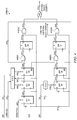
- FIG. 3 shows a phase locked loop according to the invention in which the problems of interfacing spread spectrum logic and fractional N logic are overcome.
- a reference clock divider 1 /N is provided at the input of a phase frequency detector PFD and is operable to receive a reference clock signal Ref.
- the output of the phase frequency detector is connected to a charge pump and loop filter stage CPLF, the output of which is coupled to a voltage controlled oscillator VCO.
- the voltage controlled oscillator VCO is operable to provide multiple phase outputs, which are input to an interpolator INT.
- the interpolator INT acts as a phase selector and could also be implemented, for example, as a multiplexer.
- One of the multiphase outputs of the voltage controlled oscillator VCO is selected as a synthesized frequency output.
- the interpolator INT is provided in the feedback loop of the phase locked loop so that its output is connected to a feedback divider 1 /M, with the output of the feedback divider 1 /M being fed to the feedback input of the phase frequency detector PFD.
- the output of the interpolator INT is connected to the inputs of a spread spectrum logic stage SSC, a fractional logic stage Frac-N and a logic interface circuit LOGIC X.
- the spread spectrum logic stage SSC, the fractional logic stage Frac-N and the logic interface circuit LOGIC X form a control block CB for controlling the interpolator INT to select a particular phase from the multiple phase output of the voltage controlled oscillator VCO.
- the spread spectrum logic stage SSC is operable to provide two outputs to the logic interface circuit LOGIC X; a directional control output and a phase step control output.
- the fractional logic circuitry Frac-N is operable to provide a phase step control output to the logic interface circuit LOGIC X.
- the logic interface circuit LOGIC X then provides an input to the interpolator INT based on the outputs it receives from the spread spectrum logic stage SSC and the fractional logic circuitry Frac-N.
- the spread spectrum logic stage SSC and the fractional logic stage Frac-N both receive the output from the interpolator INT selected from the multiple phase outputs of the voltage controlled oscillator VCO. It is then determined in both, the spread spectrum logic stage SSC and the fractional logic circuitry Frac-N how the interpolator INT is to be controlled in order to generate the correct next clock phase. If it is required to modulate the output frequency, the spread spectrum logic stage SSC indicates in which direction the phase of the feedback signal should be rotated using the directional control output.
- phase rotation of the signal is controlled by the directional control output signal output from the spread spectrum logic stage SSC.
- the spread spectrum logic stage SSC and the fractional logic stage Frac-N can then both indicate that discrete phase steps should be added to the feedback signal, with the phase step control signals provided at their outputs.
- both the spread spectrum logic stage SSC and the fractional logic stage Frac-N request a phase step in the same feedback clock period, in the same direction, a single phase step control control signal is passed from the logic interface circuit LOGIC X to the interpolator INT, followed by a further phase step control signal in the subsequent clock period.
- the interpolator INT then adjusts the phase of the feedback signal accordingly, so as to modulate its center frequency to the required output frequency.
- the logic interface circuit LOGIC X does not pass a phase step control signal to the interpolator INT.
- the logic interface circuit LOGIC X is shown in more detail in FIGS. 4 and 5 , with FIGS. 6 to 8 showing timing diagrams at various stages of the logic interface circuit LOGIC X.
- the logic interface circuit LOGIC X comprises two shift registers each consisting of three flip-flops DFF.
- the first shift register has a detect and set stage D&S at the set inputs of two DFFs, which is shown in detail in FIG. 5A , and is operable to receive two inputs D 01 and D 02 from the spread spectrum logic stage—the directional control signal (DIR, or D 01 ) and the phase step control signal (D 02 ), respectively.
- the second shift register has a direction detect stage D&D at its input, which is shown in detail in FIG. 5B .
- the direction detect stage D&D is also operable to receive the direction control signal and phase step control signal inputs D 01 and D 02 from the spread spectrum logic stage.
- D 07 If, however, D 07 is high during a rising edge at E 01 , D 08 will be set for a delay DLY and then it will be reset again. This means that a rising edge will be generated at D 08 . Now if D 01 is high then nothing will happen in the detect and set stage D&S during the rising edge at D 02 . However, in the direction detect stage D&D, the rising edge will be passed to D 01 as shown in FIG. 5B .
- the first shift register includes flip-flops DFF 01 , DFF 02 , DFF 03 , DFF 04 , gates AND 01 and AND 02 , as well as the detect and set stage D&S.
- This shift register works for the case when both the spread spectrum logic stage and the fractional N logic stage try to rotate the phase in the same direction, for example the clockwise direction.
- the second shift register includes flip-flops DFF 05 , DFF 06 and DFF 07 , gates AND 03 and AND 04 , as well as the direction detect stage D&D.
- the first shift register also receives a phase step control signal D 03 from the output of the fractional N stage Frac-N.
- the signal D 02 activates phase shift
- the signal D 01 determines the direction of the phase shift
- the signal D 03 initiates the phase change.
- the flip-flop DFF 01 When the signal D 03 is received at the set input of the flip-flop DFF 01 in the first shift register, the flip-flop DFF 01 is set and when the signal D 02 is received at the direction detect circuit D&D, the direction detect circuit D&D is activated. If the signal D 01 is at logic low, then the detect and set circuit D&S detects it. At the same time, it monitors the signal D 07 output from the flip-flop DFF 02 in the first shift register. If D 07 is at logic 0, then the detect and set circuit D&S will set the flip-flop DFF 02 and if D 07 is at logic 1, then the detect and set circuit D&S will set the next flip-flop in the serial shift register DFF 03 . In this case, the direction detect circuit D&D will not be activated.
- phase step control signal D 02 arrives at the direction detect circuit D&D and the signal D 01 is at logic 1, the direction detect circuit D&D detects the signal D 02 and sets the flip flop DFF 05 in the second shift register.
- the detect and set circuit D&S will not be activated in this case.
- the flip-flop contents gets shifted in the first shift register (DFF 01 ; DFF 02 ; DFF 03 ) or in the second shift register (DFF 05 ; DFF 06 ).
- the flip-flop DFF 04 in the first shift register and the flip-flop DFF 07 in the second shift register will sample logic 0 at the negative edge of the clock and the output of the logic stage LOGIC X (therefore the input to the interpolator INT) will be at logic 0. This indicates that when there is a clockwise shift and an anti-clockwise shift at the same time, there will not be any phase shift at all.
- the LOGIC X stage serves to serialize two phase shift requests, which occur at the same time at the input of the LOGIC X stage. If the fractional N stage Frac-N requests a phase shift, the request is shifted through the shift register. After three clock cycles, the corresponding phase shift is performed if no conflict arises. If the stage SSC requests a phase shift, only the second flip-flop of the corresponding shift register is set. Therefore, the required phase shift is performed after two clock cycles if no conflict occurs. Consequently, if a phase shift is requested from both stages Frac-N and from SSC at the same time, the different fixed number of clock cycles will automatically remove the conflict and spread the two requested phase shifts over two consecutive clock cycles.
- the two opposite phase shift requests create a conflict if they occur at the same time at the output of the two shift registers rather than at the input. This is due to the different fixed numbers of clock cycles the requests need to be shifted through the two registers. If the two requests in opposite directions occur at the same time at the input, two phase shifts can be performed without conflict. So, in the context of the invention, the simultaneity of two conflicting requests can relate to two requests, which are issued from the respective stages in consecutive clock cycles rather then the same.
- FIGS. 6 to 8 illustrate again three different situations for the embodiment shown in FIGS. 4 , 5 A and 5 B.
- FIG. 6 shows the situation when the spread spectrum logic stage and the fractional N stage Frac-N request a phase shift at the same time and in the same direction. This results in the output D 13 of the logic stage LOGIC X requesting a phase change from the interpolator INT at consecutive clock cycles.
- FIG. 7 shows a situation where both the spread spectrum logic stage SSC and the fractional N stage Frac-N both send a phase shift request at the same time but in opposite directions. Again, this results in the logic stage LOGIC X requesting a phase change from the interpolator INT at consecutive clock cycles. So, the circuit dissolves the conflict by providing two consecutive phase shifts as indicated by the two pulses of D 13 .
- FIG. 8 shows the case where the spread spectrum logic stage SSC and the fractional N stage Frac-N send phase change requests on consecutive clock cycles. In this case, the phase shift gets cancelled out and the output D 13 of the logic stage LOGIC X remains at logic 0.
Landscapes
- Stabilization Of Oscillater, Synchronisation, Frequency Synthesizers (AREA)
Priority Applications (1)
| Application Number | Priority Date | Filing Date | Title |
|---|---|---|---|
| US12/205,586 US7737791B2 (en) | 2007-09-05 | 2008-09-05 | Spread spectrum clocking in fractional-N PLL |
Applications Claiming Priority (5)
| Application Number | Priority Date | Filing Date | Title |
|---|---|---|---|
| DE102007042070 | 2007-09-05 | ||
| DE102007042070A DE102007042070B3 (de) | 2007-09-05 | 2007-09-05 | Spread-Spectrum-Taktung in Fraktional-N-PLLs |
| DE102007042070.8 | 2007-09-05 | ||
| US1690007P | 2007-12-27 | 2007-12-27 | |
| US12/205,586 US7737791B2 (en) | 2007-09-05 | 2008-09-05 | Spread spectrum clocking in fractional-N PLL |
Publications (2)
| Publication Number | Publication Date |
|---|---|
| US20090066423A1 US20090066423A1 (en) | 2009-03-12 |
| US7737791B2 true US7737791B2 (en) | 2010-06-15 |
Family
ID=40121759
Family Applications (1)
| Application Number | Title | Priority Date | Filing Date |
|---|---|---|---|
| US12/205,586 Active 2028-12-25 US7737791B2 (en) | 2007-09-05 | 2008-09-05 | Spread spectrum clocking in fractional-N PLL |
Country Status (5)
| Country | Link |
|---|---|
| US (1) | US7737791B2 (de) |
| EP (1) | EP2191573B1 (de) |
| AT (1) | ATE534192T1 (de) |
| DE (1) | DE102007042070B3 (de) |
| WO (1) | WO2009030742A1 (de) |
Cited By (7)
| Publication number | Priority date | Publication date | Assignee | Title |
|---|---|---|---|---|
| US20100086075A1 (en) * | 2008-07-29 | 2010-04-08 | Fujitsu Limited | Parallel Generation and Matching of a Deskew Channel |
| US20100091927A1 (en) * | 2008-07-29 | 2010-04-15 | Fujitsu Limited | Clock and Data Recovery (CDR) Using Phase Interpolation |
| US20100104057A1 (en) * | 2008-07-29 | 2010-04-29 | Fujitsu Limited | Clock and Data Recovery with a Data Aligner |
| US20100241918A1 (en) * | 2009-03-20 | 2010-09-23 | Fujitsu Limited | Clock and data recovery for differential quadrature phase shift keying |
| US8300753B2 (en) | 2008-07-29 | 2012-10-30 | Fujitsu Limited | Triple loop clock and data recovery (CDR) |
| US8952736B1 (en) * | 2013-10-09 | 2015-02-10 | Nvidia Corporation | Method and system for quantization-free and phase-dithered fractional-N generation for phase-locked-loops |
| US9244484B2 (en) | 2013-12-11 | 2016-01-26 | International Business Machines Corporation | Fractional-N spread spectrum state machine |
Families Citing this family (8)
| Publication number | Priority date | Publication date | Assignee | Title |
|---|---|---|---|---|
| US7782988B2 (en) * | 2005-05-02 | 2010-08-24 | Multigig Inc. | Digital frequency synthesizer |
| US7847643B2 (en) | 2008-11-07 | 2010-12-07 | Infineon Technologies Ag | Circuit with multiphase oscillator |
| US8638896B2 (en) * | 2010-03-19 | 2014-01-28 | Netlogic Microsystems, Inc. | Repeate architecture with single clock multiplier unit |
| US9094028B2 (en) | 2012-04-11 | 2015-07-28 | Rambus Inc. | Wide range frequency synthesizer with quadrature generation and spur cancellation |
| TWI505642B (zh) * | 2012-12-21 | 2015-10-21 | Nat Univ Chung Cheng | All - digital Spread Spectrum Clock Generation Circuit with Electromagnetic Interference Effect Decay and Its Control Method |
| WO2015172372A1 (en) * | 2014-05-16 | 2015-11-19 | Lattice Semiconductor Corporation | Fractional-n phase locked loop circuit |
| US10826738B2 (en) | 2019-01-07 | 2020-11-03 | Innophase Inc. | Systems and methods for maximizing power efficiency of a digital power amplifier in a polar transmitter |
| US10651876B1 (en) * | 2019-06-12 | 2020-05-12 | Innophase Inc. | System and method for dividing the carrier center frequency of an RF modulated signal by a non-integer divisor |
Citations (6)
| Publication number | Priority date | Publication date | Assignee | Title |
|---|---|---|---|---|
| US20050040893A1 (en) | 2003-08-20 | 2005-02-24 | Paist Kenneth W. | Spectrum profile control for a PLL and the like |
| US20050242851A1 (en) | 2004-04-29 | 2005-11-03 | Booth Richard V | Signal generator with selectable mode control |
| US7043202B2 (en) | 2002-12-06 | 2006-05-09 | Thine Electronics, Inc. | Frequency modulator apparatus of phase selection type, and frequency synthesizer of phase selection type |
| DE102005050828A1 (de) | 2004-12-22 | 2006-07-13 | Texas Instruments Deutschland Gmbh | Verfahren zur Teilung einer Frequenz durch einen Franktionalteiler und Fraktional-n-PLL |
| US7123101B2 (en) * | 2002-12-06 | 2006-10-17 | Infineon Technologies Ag | Phase locked loop comprising a ΣΔ modulator |
| US20070041486A1 (en) | 2005-08-18 | 2007-02-22 | Samsung Electronics Co., Ltd. | Semiconductor device, spread spectrum clock generator and method thereof |
-
2007
- 2007-09-05 DE DE102007042070A patent/DE102007042070B3/de active Active
-
2008
- 2008-09-05 US US12/205,586 patent/US7737791B2/en active Active
- 2008-09-05 WO PCT/EP2008/061762 patent/WO2009030742A1/en not_active Ceased
- 2008-09-05 AT AT08803731T patent/ATE534192T1/de active
- 2008-09-05 EP EP08803731A patent/EP2191573B1/de active Active
Patent Citations (6)
| Publication number | Priority date | Publication date | Assignee | Title |
|---|---|---|---|---|
| US7043202B2 (en) | 2002-12-06 | 2006-05-09 | Thine Electronics, Inc. | Frequency modulator apparatus of phase selection type, and frequency synthesizer of phase selection type |
| US7123101B2 (en) * | 2002-12-06 | 2006-10-17 | Infineon Technologies Ag | Phase locked loop comprising a ΣΔ modulator |
| US20050040893A1 (en) | 2003-08-20 | 2005-02-24 | Paist Kenneth W. | Spectrum profile control for a PLL and the like |
| US20050242851A1 (en) | 2004-04-29 | 2005-11-03 | Booth Richard V | Signal generator with selectable mode control |
| DE102005050828A1 (de) | 2004-12-22 | 2006-07-13 | Texas Instruments Deutschland Gmbh | Verfahren zur Teilung einer Frequenz durch einen Franktionalteiler und Fraktional-n-PLL |
| US20070041486A1 (en) | 2005-08-18 | 2007-02-22 | Samsung Electronics Co., Ltd. | Semiconductor device, spread spectrum clock generator and method thereof |
Cited By (11)
| Publication number | Priority date | Publication date | Assignee | Title |
|---|---|---|---|---|
| US20100086075A1 (en) * | 2008-07-29 | 2010-04-08 | Fujitsu Limited | Parallel Generation and Matching of a Deskew Channel |
| US20100091927A1 (en) * | 2008-07-29 | 2010-04-15 | Fujitsu Limited | Clock and Data Recovery (CDR) Using Phase Interpolation |
| US20100104057A1 (en) * | 2008-07-29 | 2010-04-29 | Fujitsu Limited | Clock and Data Recovery with a Data Aligner |
| US8300754B2 (en) | 2008-07-29 | 2012-10-30 | Fujitsu Limited | Clock and data recovery with a data aligner |
| US8300753B2 (en) | 2008-07-29 | 2012-10-30 | Fujitsu Limited | Triple loop clock and data recovery (CDR) |
| US8411782B2 (en) | 2008-07-29 | 2013-04-02 | Fujitsu Limited | Parallel generation and matching of a deskew channel |
| US8718217B2 (en) * | 2008-07-29 | 2014-05-06 | Fujitsu Limited | Clock and data recovery (CDR) using phase interpolation |
| US20100241918A1 (en) * | 2009-03-20 | 2010-09-23 | Fujitsu Limited | Clock and data recovery for differential quadrature phase shift keying |
| US8320770B2 (en) | 2009-03-20 | 2012-11-27 | Fujitsu Limited | Clock and data recovery for differential quadrature phase shift keying |
| US8952736B1 (en) * | 2013-10-09 | 2015-02-10 | Nvidia Corporation | Method and system for quantization-free and phase-dithered fractional-N generation for phase-locked-loops |
| US9244484B2 (en) | 2013-12-11 | 2016-01-26 | International Business Machines Corporation | Fractional-N spread spectrum state machine |
Also Published As
| Publication number | Publication date |
|---|---|
| DE102007042070B3 (de) | 2009-01-15 |
| US20090066423A1 (en) | 2009-03-12 |
| ATE534192T1 (de) | 2011-12-15 |
| WO2009030742A1 (en) | 2009-03-12 |
| EP2191573B1 (de) | 2011-11-16 |
| EP2191573A1 (de) | 2010-06-02 |
Similar Documents
| Publication | Publication Date | Title |
|---|---|---|
| US7737791B2 (en) | Spread spectrum clocking in fractional-N PLL | |
| US8638144B1 (en) | Systems and methods involving phase detection with adaptive locking/detection features | |
| US7994828B2 (en) | Frequency divider, frequency dividing method thereof, and phase locked loop utilizing the frequency divider | |
| US8664985B2 (en) | Phase frequency detector and charge pump for phase lock loop fast-locking | |
| EP1323233B1 (de) | Synchronisierter digitaler mehrfachausgang-taktmanager | |
| US7847643B2 (en) | Circuit with multiphase oscillator | |
| KR20140112656A (ko) | 디지털 위상 고정 루프 | |
| EP2814177B1 (de) | Phasenregelkreisvorrichtung mit Synchronisierungsmitteln | |
| US8354862B2 (en) | Phase-lock assistant circuitry | |
| US10784844B2 (en) | Fractional frequency divider and frequency synthesizer | |
| US10312923B2 (en) | Electronic circuit, phase-locked loop, transceiver circuit, radio station and method of frequency dividing | |
| US9735788B2 (en) | Phase locked loop for reducing fractional spur noise | |
| JPH11316616A (ja) | クロック信号を供給するための方法及び装置 | |
| EP3190705B1 (de) | Fraktionierte pll mit einem linearem pfd mit einstellbarer verzögerung | |
| US11817863B2 (en) | Fractional-n sub-sampling phase locked loop using phase rotator | |
| US7035367B2 (en) | Fractional multi-modulus prescaler | |
| US11632119B1 (en) | Programmable fractional ripple divider | |
| US8040996B2 (en) | Method and system for RF signal generation utilizing a synchronous multi-modulus divider | |
| US10484027B2 (en) | Glitch free phase selection multiplexer enabling fractional feedback ratios in phase locked loops | |
| JP3267945B2 (ja) | 周波数シンセサイザ装置と周波数生成方法 | |
| CN114337661A (zh) | 基于pll电路的小数分频和动态移相系统 | |
| Bhambore et al. | Dynamically reconfiguration of PLL using FPGA | |
| JPH1174788A (ja) | Pll回路 |
Legal Events
| Date | Code | Title | Description |
|---|---|---|---|
| AS | Assignment |
Owner name: TEXAS INSTRUMENTS INCORPORATED, GERMANY Free format text: ASSIGNMENT OF ASSIGNORS INTEREST;ASSIGNORS:SAREEN, PUNEET;SEIBOLD, HERMANN;REEL/FRAME:021862/0437 Effective date: 20081021 Owner name: TEXAS INSTRUMENTS INCORPORATED,GERMANY Free format text: ASSIGNMENT OF ASSIGNORS INTEREST;ASSIGNORS:SAREEN, PUNEET;SEIBOLD, HERMANN;REEL/FRAME:021862/0437 Effective date: 20081021 |
|
| AS | Assignment |
Owner name: TEXAS INSTRUMENTS DEUTSCHLAND GMBH,GERMANY Free format text: CORRECTIVE ASSIGNMENT TO CORRECT THE ASSIGNEE TO REFLECT "TEXAS INSTRUMENTS DEUTSCHLAND GMBH." PREVIOUSLY RECORDED ON REEL 021862 FRAME 0437. ASSIGNOR(S) HEREBY CONFIRMS THE CHANGE. PUNEET SAREEN AND HERMANN SEIBOLD CONFIRM THE CHANGE FROM "TEXAS INSTRUMENTS INCORPORATED";ASSIGNORS:SAREEN, PUNEET;SEIBOLD, HERMANN;REEL/FRAME:024309/0913 Effective date: 20081021 |
|
| STCF | Information on status: patent grant |
Free format text: PATENTED CASE |
|
| FPAY | Fee payment |
Year of fee payment: 4 |
|
| MAFP | Maintenance fee payment |
Free format text: PAYMENT OF MAINTENANCE FEE, 8TH YEAR, LARGE ENTITY (ORIGINAL EVENT CODE: M1552) Year of fee payment: 8 |
|
| AS | Assignment |
Owner name: TEXAS INSTRUMENTS INCORPORATED, TEXAS Free format text: ASSIGNMENT OF ASSIGNORS INTEREST;ASSIGNOR:TEXAS INSTRUMENTS DEUTSCHLAND GMBH;REEL/FRAME:055314/0255 Effective date: 20210215 |
|
| MAFP | Maintenance fee payment |
Free format text: PAYMENT OF MAINTENANCE FEE, 12TH YEAR, LARGE ENTITY (ORIGINAL EVENT CODE: M1553); ENTITY STATUS OF PATENT OWNER: LARGE ENTITY Year of fee payment: 12 |