US8022365B2 - Charged particle beam equipments, and charged particle beam microscope - Google Patents
Charged particle beam equipments, and charged particle beam microscope Download PDFInfo
- Publication number
- US8022365B2 US8022365B2 US12/168,940 US16894008A US8022365B2 US 8022365 B2 US8022365 B2 US 8022365B2 US 16894008 A US16894008 A US 16894008A US 8022365 B2 US8022365 B2 US 8022365B2
- Authority
- US
- United States
- Prior art keywords
- charged particle
- particle beam
- diffraction pattern
- size
- illumination
- Prior art date
- Legal status (The legal status is an assumption and is not a legal conclusion. Google has not performed a legal analysis and makes no representation as to the accuracy of the status listed.)
- Active, expires
Links
Images


Classifications
-
- H—ELECTRICITY
- H01—ELECTRIC ELEMENTS
- H01J—ELECTRIC DISCHARGE TUBES OR DISCHARGE LAMPS
- H01J37/00—Discharge tubes with provision for introducing objects or material to be exposed to the discharge, e.g. for the purpose of examination or processing thereof
- H01J37/26—Electron or ion microscopes; Electron or ion diffraction tubes
- H01J37/295—Electron or ion diffraction tubes
Definitions
- the present invention relates to charged particle beam equipment such as an electron microscope and an ion microscope.
- phase retrieval method or a Fourier iterative phase retrieval method (R. W. Gerchberg and W. O. Saxton, “A practical algorithm for the determination of phase from image and diffraction plane pictures”, Optik, vol. 35, pp. 237-246, 1972) is a method (hereinafter, referred to as “phase retrieval method” in this specification) for reconstructing an object image from a diffraction pattern.
- a diffraction pattern can be obtained without using a lens, so that, in the phase retrieval method, it can be expected to observe an image with a high resolution and without the influence of the aberrations of the lens.
- a technique for reproducing an object image from a diffraction pattern using the phase retrieval method has been advanced, which enables an image observation with a resolution of about the wavelength.
- an example of applying the phase retrieval method to an electron microscope has been reported (J. M. Zuo et al., “Atomic Resolution Imaging of a Carbon Nanotube from Diffraction Intensities”, Science, Vol. 300, pp. 1419-1421, 2003).
- An image observed by a microscope intrinsically contains information of its amplitude and phase. However, the observed intensity of the image is the square of the amplitude, and the phase information does not appear directly in a normal observation method. This fact is also true in an object space where an object image is observed and in a reciprocal space where a diffraction pattern is observed.
- the object space and the reciprocal space have the following relation. That is, if the amplitude and phase information can be completely obtained in one of the spaces, the other one can be completely reproduced by the Fourier transform in a mathematical sense.
- the phase retrieval method is a method to reconstruct an object image, in which a diffraction pattern is obtained by observation and the phase of the reciprocal space is obtained by calculation.
- the amplitude that is the square root of the observed diffraction pattern is set as a constraint condition of the reciprocal space, and some kind of constraint condition is set in the object space, so that the phase is reproduced little by little while repeating the Fourier transform and inverse Fourier transform.
- the “reconstructed image” represents an object space image in process of phase retrieval procedure
- the “magnified image” represents an image of the object space observed by a microscope.
- the “object image” essentially represents the whole image of the object space including the “reconstructed image” and the “magnified image”.
- the final result obtained by the phase retrieval method is referred to as the “object image”.
- FIG. 1 An iteration procedure will be schematically shown in FIG. 1 .
- some kind of image for example, a random pattern, a low resolution magnified image, or the like
- F(k) an amplitude
- ⁇ a phase
- the amplitude information is replaced by that (F′(k) that is referred to as a constraint condition in the reciprocal space) of the diffraction pattern obtained by observation to perform the Fourier transform again (which is performed as the inverse Fourier transform with respect to the former Fourier transform).
- amplitude (f′(x)) information and the phase ( ⁇ ) information of the object space obtained by the inverse Fourier transform while the phase information is left as it is, a result (f(x)) obtained by applying some kind of constraint condition (for example, the amplitude information except for the area of a specimen is set to 0) to the amplitude information is Fourier transformed.
- some kind of constraint condition for example, the amplitude information except for the area of a specimen is set to 0
- the amplitude is replaced by that of the diffraction pattern to perform the Fourier transform, thus obtaining the amplitude and phase information of the object space.
- the phase information of the reciprocal space is reproduced.
- the amplitude information of the diffraction pattern and the phase information are inverse Fourier transformed to reconstruct an object image.
- phase retrieval Since the phases in both of the reciprocal space and the object space can be reproduced in process of the phase retrieval, it is possible to obtain the phase image of the object space by using the phase retrieval method. Further, it is possible to visualize an electric field and a magnetic field which are conventionally obtained by an electron beam holography or other methods.
- a diffraction pattern can be obtained in such a manner that beams that are substantially parallel to each other are illuminated on a specimen and the beams that pass through the specimen (or reflected beams) are detected at a sufficiently-far position. Therefore, a lens is not essentially required on the back side (the side opposite to an optical source along the optical axis) of the specimen. At this time, a distance from the specimen to a detection plane is referred to as a camera length.
- a lens effect of an objective lens on the back side of the specimen is generally utilized in an electron microscope, and the diffraction pattern formed at a back focal plane is magnified by a subsequent lens (projection lens).
- the camera length in this case is defined depending on a position apart from the specimen where the same diffraction spot intervals can be obtained in the case where the above-described lens is not present.
- an image size F of the object image to be reconstructed is obtained by following formula (1) using a camera length L, a pixel size p of a detector for detecting the diffraction pattern, and a wavelength ⁇ of the electron beam determined on the basis of an acceleration voltage.
- F 2 ⁇ L/p (1)
- the wavelength, the camera length, and the pixel size are changed due to the following reasons in accordance with the material of the specimen to be observed and the resolution to be required.
- the image size F of the object image to be reconstructed by the Fourier transform is not constant and is changed for each observation condition.
- the diffraction pattern reflects all information of a specimen area on which the beam is illuminated.
- the image size obtained by performing the Fourier transform for the diffraction pattern is accordingly changed.
- the specimen information forming the diffraction pattern is not equal to the object image reconstructed from the diffraction pattern.
- phase retrieval method when actually applying the phase retrieval method to the charged particle beam microscope, following way of observation is appropriate: a method using a normal lens is utilized for observing movement to determine the position of the specimen to be observed and for roughly observing a structure and the phase retrieval method is applied in the case of obtaining a higher resolution.
- time reduction in the object image reconstruction is practically required.
- charged particle beam equipment or a charged particle beam microscope of the present invention includes an illumination adjustment system which allows the area of a beam illuminated on a specimen for obtaining a diffraction pattern to have a certain relation with the image size of an object image to be reconstructed even in the case where the wavelength of the charged particle beam, a camera length at the time of obtaining the diffraction pattern, and the pixel size of a diffraction pattern detector are changed.
- charged particle beam equipment or a charged particle beam microscope of the present invention includes a deflector which scans a specimen with an illumination beam, and which allows a deflection width with which the specimen is scanned to have a certain relation with an image size determined by the wavelength of the charged particle beam, a camera length at the time of obtaining a diffraction pattern, and the pixel size of a diffraction pattern detector.
- the illumination area on the specimen for obtaining the diffraction pattern is substantially equal to the size of the image reconstructed by the phase retrieval method, so that the diffraction pattern is substantially equal, in a mathematical sense, to the object image to be reconstructed in just proportion of information.
- the phase retrieval method is performed using the magnified image that has a certain relation, in size, with the image obtained by performing the Fourier transform for the diffraction pattern, so that the converge of the calculation becomes faster, and the accuracy is enhanced.
- FIG. 1 is a diagram showing a processing procedure of a phase retrieval method
- FIGS. 2A and 2B are schematic diagrams showing main constituent elements of a scanning electron microscope according to a first embodiment
- FIG. 3 is a diagram showing a case in which an illumination area on a specimen is specified by two illumination lenses in the first embodiment
- FIGS. 4A and 4B are schematic diagrams showing main constituent elements of a transmission electron microscope according to a second embodiment
- FIG. 5 is a diagram showing a case in which an illumination area on a specimen is specified by two illumination lenses in the second embodiment.
- FIG. 6 is a diagram showing an example of a graphical user interface when the phase retrieval method is applied in the embodiments.
- the present invention can be applied to not only a scanning electron microscope, but also charged particle beam equipment such as a microscope using charged particles such as an electron microscope and an ion beam microscope including a transmission electron microscope.
- SEM scanning electron microscope
- STEM scanning transmission electron microscope
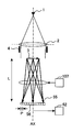
- FIGS. 2A and 2B are schematic diagrams of a scanning electron microscope and a scanning transmission electron microscope according to the first embodiment.
- An electron beam emitted from an electron source 1 is illuminated on a specimen 3 through an illumination lens 2 .
- a magnified image is observed by displaying on an image display unit 105 in such a manner that the beam is converged on the specimen 3 through the illumination lens 2 and scanned on the specimen 3 or the vicinity of the specimen 3 by a deflector 4 , and an electron beam 53 , which passes through the specimen 3 and is detected by a transmission electron detector 51 , or a secondary electron/reflection electron 54 , which is generated from the specimen 3 and is detected by a secondary electron/reflection electron detector 52 , is synchronized with a deflection signal of the deflector 4 .
- a scanning transmission electron microscope STEM obtains an image with the beam which passes through the specimen using the transmission electron detector 51 .
- a high voltage power supply 101 controls an acceleration voltage, an extraction voltage and an extraction current of the electron source 1 .
- An illumination lens control circuit 102 controls the intensity of the illumination lens 2
- a deflection signal control circuit 103 controls the deflector 4 .
- the signal detected by the transmission electron detector 51 or the secondary electron/reflection electron detector 52 is amplified by an amplifier 61 and the amplified signal is synchronized with the deflection signal of the deflection signal control circuit 103 in an image processor 104 to be displayed on the image display unit 105 as a magnified image.
- the image synchronized with the deflection signal is also recorded into an image recording section 106 .
- the high voltage power supply 101 , the illumination lens control circuit 102 , and the deflection signal control circuit 103 are controlled by an overall control system 110 that is a control unit for the whole equipment.
- a diffraction pattern 55 is obtained in such a manner that parallel beams from the illumination lens 2 are illuminated on the specimen 3 and the diffraction pattern is detected by a diffraction pattern detector 56 which is located sufficiently apart from the specimen 3 .
- a camera length L at this time is defined by a length between the specimen 3 and the diffraction pattern detector 56 .
- the camera length L is adjusted by a projection lens 7 .
- the projection lens 7 is controlled by a projection lens control circuit 107 .
- the projection lens control circuit 107 is also controlled by the overall control system 110 .
- a CCD camera, an imaging plate, a film or the like is used for the diffraction pattern detector 56 .
- the obtained diffraction pattern is digitized to be recorded into a diffraction recording section 62 .
- the minimum unit of the digitized pattern is referred to as a pixel size p.
- the pixel size p is the same as that of the CCD camera in some cases.
- a phase retrieval process is performed for the recorded diffraction pattern in a computer 63 , such as a personal computer, that is a processor for processing digital data.
- the magnified image recorded into the image recording section 106 can be used as an initial condition or an object space constraint condition.
- a result of the phase retrieval process performed by the computer 63 is displayed on the image display unit 105 .
- the magnified image recorded into the image recording section 106 may be displayed as it is on the image display unit 105 .
- the reconstructed image reconstructed by the phase retrieval method can be obtained by performing the Fourier transform for the diffraction pattern obtained by observation. Therefore, an image size F of the reconstructed image is determined by the formula (1).
- an illumination area so as to be substantially equal to the image size F.
- the illumination area can be associated with the object image by setting the illumination area at a constant magnification ratio of the image size F if the acceleration voltage and the camera length are changed.
- an illumination adjustment system 201 is provided in the embodiment so as to adjust a beam illumination area in the case where a wavelength ⁇ of the electron beam, the camera length L, and the pixel size p are changed.
- the illumination adjustment system 201 obtains wavelength information of the illumination beam, camera length information, and pixel size information from the high voltage power supply 101 , the projection lens control circuit 107 , and the diffraction recording section 62 , respectively, so as to set the illumination area corresponding to the image size determined by the formula (1), and transmits the control information to an aperture control circuit 202 to be described later, the illumination lens control circuit 102 , and the deflection signal control circuit 103 .
- FIG. 2A shows an adjustment system using an aperture AP.
- the aperture adjustment system 202 adjusts at least one of an opening size of the aperture AP, a position along an optical axis AX, and rotation in an aperture plane by using the control information from the illumination adjustment system 201 .
- the opening of the aperture is usually circular in shape, it is desirable that the illumination area on the specimen is rectangular in shape in order to correspond to the diffraction pattern. Therefore, the opening of the aperture AP can be set to have a rectangular shape. In addition, it is desirable that the aperture AP has a rotation mechanism in the aperture plane so that the opening of the aperture can be rotated on the specimen.
- FIG. 3 shows an adjustment system configured by plural illumination lenses (a first illumination lens 21 and a second illumination lens 22 ).
- the control information from the illumination adjustment system 201 is transmitted to the illumination lens control circuit 102 , and the illumination area is adjusted by controlling the first illumination lens 21 and the second illumination lens 22 .
- phase retrieval method is applied to the scanning electron microscope (SEM) as in the embodiment, it is preferable to observe the specimen as with a normal SEM up to a certain level of resolution (magnification), and to use the phase retrieval method when further increasing the resolution.
- SEM scanning electron microscope
- the magnified image that is substantially equal in size to the image obtained by performing the Fourier transform for the diffraction pattern is used, so that the magnified image can be applied to the calculation as it is, and a calculation process can be performed at a high speed. Further, since the phase retrieval image and the image obtained by the SEM observation have a good relation in continuity, a user can observe with the feeling of less discomfort.
- the control information from the illumination adjustment system 201 is reflected on the deflector 4 used when obtaining the magnified image in FIG. 2A .
- the control information from the illumination adjustment system 201 is transmitted to the deflection signal control circuit 103 to change at least one of the deflection width and the deflection rotation of the deflector 4 , and to adjust the illumination area on the specimen so as to correspond to the reconstructed image. Accordingly, it is possible to perform the phase retrieval method using the magnified image that is substantially equal in size to the image obtained by performing the Fourier transform for the diffraction pattern, the converge of the calculation becomes faster, and the accuracy is enhanced.
- the illumination adjustment system 201 which transmits the control information to the aperture control circuit 202 , the illumination lens control circuit 102 , and the deflection signal control circuit 103 is provided separately from the overall control system 110 that is an overall control unit.
- the function of the illumination adjustment system 201 may be included in the overall control system 110 .
- the wavelength information, the camera length information, and the pixel size information to be required are transmitted to the overall control system 110 , and the overall control system 110 generates the control information to the aperture control circuit 202 .
- FIGS. 4A and 4B are schematic diagrams, each showing a transmission electron microscope according to a second embodiment.
- the electron beam emitted from the electron source 1 is illuminated on the specimen 3 through the illumination lens 2 and a front-field lens effect OB 1 of the objective lens.
- OB 1 a front-field lens effect of the objective lens.
- the diffraction pattern can be obtained ( FIG. 4A ) and the magnified image can be observed ( FIG. 4B ).
- the specimen image is magnified about ten times by a back-field lens effect OB 2 of the objective lens, and the magnified image is further magnified and projected on a detection plane 57 by the projection lens 7 , as shown in FIG. 4B .
- the lens effects OB 1 and OB 2 are collectively referred to as the objective lens OB.
- the diffraction pattern formed on a back focal plane of the back-field lens effect OB 2 of the objective lens is magnified and projected on the detection plane 57 by the projection lens, as shown in FIG. 4A .
- a camera length L′ can be obtained by converting a diffraction spot interval d in the detection plane 57 into a case in which the diffraction pattern is obtained without using a lens.
- the beam illumination area on the specimen can be adjusted by changing the intensities of the illumination lens 2 and the front-field lens effect OB 1 of the objective lens 2 using the illumination adjustment system, as similar to the first embodiment.
- the beam illumination area on the specimen 3 can be adjusted by adjusting the first illumination lens 21 and the second illumination lens 22 while keeping constant the condition of the objective lens OB.
- the constituent elements subsequent to the back-field lens effect OB 2 of the objective lens are omitted.
- the shape of the beam illumination area on the specimen 3 can be set depending on the opening shape of the aperture AP, as similar to the first embodiment. In this case, it is desirable that a conjugate image of the aperture AP is formed on the specimen 3 . As similar to the first embodiment, it is desirable that the aperture AP has a rotation mechanism in the aperture plane so as to rotate the opening shape of the aperture on the specimen.
- FIG. 6 is an example of a Graphical User Interface (GUI) in the electron microscope of each of the first and second embodiments.
- GUI Graphical User Interface
- a graphical user interface 300 is included in the overall control system 110 shown in each of FIGS. 2A and 3 , and includes an object space image display unit 301 and a diffraction pattern display unit 302 .
- the magnified image, the reconstructed image in process of the phase retrieval, and the object image as a final result are displayed on the object space image display unit 301 , and the diffraction pattern obtained by observation (the image recorded into the diffraction recording section 62 in each of FIGS. 2A , 2 B and 3 ) is displayed on the diffraction pattern display unit 302 .
- the graphical user interface 300 further includes an acceleration voltage display unit 303 , a camera length display unit 304 , and a pixel size display unit 305 which respectively display the acceleration voltage of the illumination beam, the camera length, and the pixel size of the diffraction pattern detector. These values indicate the acceleration voltage information, the camera length information, and the pixel size information in the high voltage power supply 101 , the projection lens control circuit 107 , and the diffraction recording section 62 in each of FIGS. 2A , 2 B and 3 .
- the acceleration voltage, the camera length, and the pixel size can be input by a user, and these input values can be transmitted to the illumination adjustment system 201 to be reflected on the illumination condition.
- the graphical user interface 300 is included in the overall control system 110 shown in each of FIGS. 2A and 3 .
- the image display unit 105 shown in each of FIGS. 2A and 3 can be configured to display the graphical user interface 300 .
Landscapes
- Chemical & Material Sciences (AREA)
- Analytical Chemistry (AREA)
- Analysing Materials By The Use Of Radiation (AREA)
Applications Claiming Priority (2)
| Application Number | Priority Date | Filing Date | Title |
|---|---|---|---|
| JP2007184084A JP5462434B2 (ja) | 2007-07-13 | 2007-07-13 | 荷電粒子ビーム装置、及び荷電粒子ビーム顕微鏡 |
| JP2007-184084 | 2007-07-13 |
Publications (2)
| Publication Number | Publication Date |
|---|---|
| US20090014651A1 US20090014651A1 (en) | 2009-01-15 |
| US8022365B2 true US8022365B2 (en) | 2011-09-20 |
Family
ID=39884411
Family Applications (1)
| Application Number | Title | Priority Date | Filing Date |
|---|---|---|---|
| US12/168,940 Active 2029-07-14 US8022365B2 (en) | 2007-07-13 | 2008-07-08 | Charged particle beam equipments, and charged particle beam microscope |
Country Status (3)
| Country | Link |
|---|---|
| US (1) | US8022365B2 (de) |
| EP (1) | EP2015342B1 (de) |
| JP (1) | JP5462434B2 (de) |
Cited By (1)
| Publication number | Priority date | Publication date | Assignee | Title |
|---|---|---|---|---|
| US20160163501A1 (en) * | 2014-12-04 | 2016-06-09 | Jeol Ltd. | Charged Particle Beam Device and Image Acquisition Method |
Families Citing this family (8)
| Publication number | Priority date | Publication date | Assignee | Title |
|---|---|---|---|---|
| EP2261947A4 (de) * | 2008-04-04 | 2015-05-20 | Hitachi Ltd | Diffraktionsbilderfassungsverfahren und vorrichtung zur abstrahlung geladener teilchen |
| JP2011243540A (ja) * | 2010-05-21 | 2011-12-01 | Hitachi High-Technologies Corp | 透過電子顕微鏡の制限視野絞りプレート、制限視野絞りプレートの製造方法及び制限視野電子回折像の観察方法 |
| JPWO2011155122A1 (ja) * | 2010-06-07 | 2013-08-01 | 株式会社日立ハイテクノロジーズ | 回路パターン検査装置およびその検査方法 |
| NL2009367C2 (en) * | 2012-08-27 | 2014-03-03 | Stichting Vu Vumc | Microscopic imaging apparatus and method to detect a microscopic image. |
| KR101613884B1 (ko) * | 2015-01-27 | 2016-04-20 | 기초과학연구원 | 위상 조절을 통한 엑스선 회절 현미경 장치 및 엑스선 회절 방법 |
| EP3073508B1 (de) * | 2015-03-27 | 2020-09-16 | Carl Zeiss Microscopy GmbH | Verfahren zur erzeugung einer zoomfolge und mikroskopsystem, das zur durchführung des verfahrens ausgestaltet ist |
| EP3474308A1 (de) * | 2017-10-17 | 2019-04-24 | Universiteit Antwerpen | Räumliche phasenmanipulation eines geladenen teilchenstrahls |
| KR102826526B1 (ko) * | 2024-07-04 | 2025-06-27 | 한국기초과학지원연구원 | 전자빔 방출 특성 분석을 위한 전자 현미경 장치 및 방법 |
Citations (6)
| Publication number | Priority date | Publication date | Assignee | Title |
|---|---|---|---|---|
| US4160162A (en) * | 1976-11-12 | 1979-07-03 | Siemens Aktiengesellschaft | Method for the pictorial display of a diffraction image in a transmission-type, scanning, corpuscular-beam microscope |
| US4651220A (en) * | 1984-10-12 | 1987-03-17 | Fuji Photo Film Co., Ltd. | Method of recording and reproducing images produced by an electron microscope |
| US5753913A (en) * | 1995-10-03 | 1998-05-19 | U.S. Philips Corporation | Method of reconstructing an image in a particle-optical apparatus |
| US20020099573A1 (en) * | 2001-01-24 | 2002-07-25 | Hitachi, Ltd. | Network solution system of analysis and evaluation |
| US20050253069A1 (en) * | 2004-04-02 | 2005-11-17 | California Institute Of Technology | Method and system for ultrafast photoelectron microscope |
| WO2005114693A1 (ja) | 2004-05-20 | 2005-12-01 | National University Corporation Hokkaido University | 電子顕微方法およびそれを用いた電子顕微鏡 |
Family Cites Families (4)
| Publication number | Priority date | Publication date | Assignee | Title |
|---|---|---|---|---|
| JPH0793119B2 (ja) * | 1988-06-17 | 1995-10-09 | 日本電子株式会社 | 電子顕微鏡 |
| JP2005235665A (ja) * | 2004-02-23 | 2005-09-02 | Hitachi High-Technologies Corp | 暗視野走査透過電子顕微鏡および観察方法 |
| JP4726048B2 (ja) * | 2005-05-27 | 2011-07-20 | 株式会社日立製作所 | 位相回復方式の電子顕微鏡による観察方法 |
| JP4337832B2 (ja) * | 2006-03-06 | 2009-09-30 | 株式会社日立製作所 | 電子線を用いた観察装置及び観察方法 |
-
2007
- 2007-07-13 JP JP2007184084A patent/JP5462434B2/ja active Active
-
2008
- 2008-07-08 EP EP08012309.4A patent/EP2015342B1/de active Active
- 2008-07-08 US US12/168,940 patent/US8022365B2/en active Active
Patent Citations (12)
| Publication number | Priority date | Publication date | Assignee | Title |
|---|---|---|---|---|
| US4160162A (en) * | 1976-11-12 | 1979-07-03 | Siemens Aktiengesellschaft | Method for the pictorial display of a diffraction image in a transmission-type, scanning, corpuscular-beam microscope |
| US4651220A (en) * | 1984-10-12 | 1987-03-17 | Fuji Photo Film Co., Ltd. | Method of recording and reproducing images produced by an electron microscope |
| US5753913A (en) * | 1995-10-03 | 1998-05-19 | U.S. Philips Corporation | Method of reconstructing an image in a particle-optical apparatus |
| US20020099573A1 (en) * | 2001-01-24 | 2002-07-25 | Hitachi, Ltd. | Network solution system of analysis and evaluation |
| US20050253069A1 (en) * | 2004-04-02 | 2005-11-17 | California Institute Of Technology | Method and system for ultrafast photoelectron microscope |
| US7154091B2 (en) * | 2004-04-02 | 2006-12-26 | California Institute Of Technology | Method and system for ultrafast photoelectron microscope |
| US20080017796A1 (en) * | 2004-04-02 | 2008-01-24 | California Institute Of Technology | Method and system for ultrafast photoelectron microscope |
| US7442931B2 (en) * | 2004-04-02 | 2008-10-28 | California Institute Of Technology | Method and system for ultrafast photoelectron microscope |
| US20090236521A1 (en) * | 2004-04-02 | 2009-09-24 | California Institute Of Technology | Method and system for ultrafast photoelectron microscope |
| US7915583B2 (en) * | 2004-04-02 | 2011-03-29 | California Institute Of Technology | Method and system for ultrafast photoelectron microscope |
| WO2005114693A1 (ja) | 2004-05-20 | 2005-12-01 | National University Corporation Hokkaido University | 電子顕微方法およびそれを用いた電子顕微鏡 |
| EP1768161A1 (de) | 2004-05-20 | 2007-03-28 | National University Corporation Hokkaido University | Elektronenmikroskopisches verfahren und elektronenmikroskop damit |
Non-Patent Citations (2)
| Title |
|---|
| J.M. Zuo et al., Atomic Resolution Imaging of a Carbon Nanotube from Diffraction Intensities, (2003), Science, vol. 300, pp. 1419-1421. |
| R.W. Gerchberg et al., A Practical Algorithm for the Determination of Phase from Image and Diffraction Plan Pictures, Optik, (1972) vol. 35, pp. 237-246. |
Cited By (1)
| Publication number | Priority date | Publication date | Assignee | Title |
|---|---|---|---|---|
| US20160163501A1 (en) * | 2014-12-04 | 2016-06-09 | Jeol Ltd. | Charged Particle Beam Device and Image Acquisition Method |
Also Published As
| Publication number | Publication date |
|---|---|
| EP2015342A2 (de) | 2009-01-14 |
| EP2015342B1 (de) | 2016-02-17 |
| US20090014651A1 (en) | 2009-01-15 |
| JP2009021156A (ja) | 2009-01-29 |
| EP2015342A3 (de) | 2014-09-10 |
| JP5462434B2 (ja) | 2014-04-02 |
Similar Documents
| Publication | Publication Date | Title |
|---|---|---|
| US8022365B2 (en) | Charged particle beam equipments, and charged particle beam microscope | |
| EP2315232B1 (de) | Transmissionselektronenmikroskop und Verfahren zur Untersuchung einer Probe | |
| Mayo et al. | Quantitative X‐ray projection microscopy: phase‐contrast and multi‐spectral imaging | |
| Erni et al. | Atomic-resolution imaging with a sub-50-pm electron probe | |
| JP3281017B2 (ja) | 荷電粒子ビーム装置 | |
| US6448556B1 (en) | Atomic focusers in electron microscopy | |
| JP5736461B2 (ja) | 電子顕微鏡および試料観察方法 | |
| JP5106627B2 (ja) | 回折像取得方法、及び荷電粒子線装置 | |
| CN107622933B (zh) | 使用叠层成像术对样本成像的方法 | |
| JP2017009603A (ja) | タイコグラフィックイメージングの方法 | |
| EP4067886B1 (de) | Verfahren und system zur bestimmung einer kristallstruktur | |
| Geiger et al. | Electron holography with a Cs-corrected transmission electron microscope | |
| JP4852758B2 (ja) | 電子顕微方法およびそれを用いた電子顕微鏡 | |
| JP2007115409A (ja) | 電子線干渉装置および電子顕微鏡 | |
| Kamimura et al. | 10-kV diffractive imaging using newly developed electron diffraction microscope | |
| McCartney et al. | Differential phase contrast in TEM | |
| Tanji et al. | Differential microscopy by conventional electron off‐axis holography | |
| JP4726048B2 (ja) | 位相回復方式の電子顕微鏡による観察方法 | |
| Zheng et al. | Fast imaging with inelastically scattered electrons by off-axis chromatic confocal electron microscopy | |
| He et al. | A method of combining STEM image with parallel beam diffraction and electron-optical conditions for diffractive imaging | |
| Kirkland et al. | Transmission electron microscopy without aberrations: Applications to materials science | |
| Latychevskaia et al. | Bragg holography of nano-crystals | |
| JP7376798B2 (ja) | 荷電粒子線像生成装置、荷電粒子線装置、荷電粒子線像生成方法およびプログラム | |
| JPH0721965A (ja) | 電子ビーム装置における物体構造試験方法及び装置 | |
| Thesen et al. | Low Voltage Nanotip Interferometry |
Legal Events
| Date | Code | Title | Description |
|---|---|---|---|
| AS | Assignment |
Owner name: HITACHI, LTD., JAPAN Free format text: ASSIGNMENT OF ASSIGNORS INTEREST;ASSIGNORS:KAMIMURA, OSAMU;OHTA, HIROYA;REEL/FRAME:021202/0210;SIGNING DATES FROM 20080612 TO 20080616 Owner name: HITACHI, LTD., JAPAN Free format text: ASSIGNMENT OF ASSIGNORS INTEREST;ASSIGNORS:KAMIMURA, OSAMU;OHTA, HIROYA;SIGNING DATES FROM 20080612 TO 20080616;REEL/FRAME:021202/0210 |
|
| STCF | Information on status: patent grant |
Free format text: PATENTED CASE |
|
| FEPP | Fee payment procedure |
Free format text: PAYOR NUMBER ASSIGNED (ORIGINAL EVENT CODE: ASPN); ENTITY STATUS OF PATENT OWNER: LARGE ENTITY |
|
| FPAY | Fee payment |
Year of fee payment: 4 |
|
| AS | Assignment |
Owner name: HITACHI HIGH-TECHNOLOGIES CORPORATION, JAPAN Free format text: ASSIGNMENT OF ASSIGNORS INTEREST;ASSIGNOR:HITACHI, LTD.;REEL/FRAME:046256/0666 Effective date: 20180131 |
|
| MAFP | Maintenance fee payment |
Free format text: PAYMENT OF MAINTENANCE FEE, 8TH YEAR, LARGE ENTITY (ORIGINAL EVENT CODE: M1552); ENTITY STATUS OF PATENT OWNER: LARGE ENTITY Year of fee payment: 8 |
|
| AS | Assignment |
Owner name: HITACHI HIGH-TECH CORPORATION, JAPAN Free format text: CHANGE OF NAME AND ADDRESS;ASSIGNOR:HITACHI HIGH-TECHNOLOGIES CORPORATION;REEL/FRAME:052259/0227 Effective date: 20200212 |
|
| MAFP | Maintenance fee payment |
Free format text: PAYMENT OF MAINTENANCE FEE, 12TH YEAR, LARGE ENTITY (ORIGINAL EVENT CODE: M1553); ENTITY STATUS OF PATENT OWNER: LARGE ENTITY Year of fee payment: 12 |