US8073892B2 - Cryptographic system, method and multiplier - Google Patents
Cryptographic system, method and multiplier Download PDFInfo
- Publication number
- US8073892B2 US8073892B2 US11/323,994 US32399405A US8073892B2 US 8073892 B2 US8073892 B2 US 8073892B2 US 32399405 A US32399405 A US 32399405A US 8073892 B2 US8073892 B2 US 8073892B2
- Authority
- US
- United States
- Prior art keywords
- operand
- bits
- multiplier
- multipliers
- logic
- Prior art date
- Legal status (The legal status is an assumption and is not a legal conclusion. Google has not performed a legal analysis and makes no representation as to the accuracy of the status listed.)
- Expired - Fee Related, expires
Links
Images


Classifications
-
- G—PHYSICS
- G06—COMPUTING OR CALCULATING; COUNTING
- G06F—ELECTRIC DIGITAL DATA PROCESSING
- G06F7/00—Methods or arrangements for processing data by operating upon the order or content of the data handled
- G06F7/38—Methods or arrangements for performing computations using exclusively denominational number representation, e.g. using binary, ternary, decimal representation
- G06F7/48—Methods or arrangements for performing computations using exclusively denominational number representation, e.g. using binary, ternary, decimal representation using non-contact-making devices, e.g. tube, solid state device; using unspecified devices
- G06F7/52—Multiplying; Dividing
- G06F7/523—Multiplying only
- G06F7/527—Multiplying only in serial-parallel fashion, i.e. one operand being entered serially and the other in parallel
- G06F7/5272—Multiplying only in serial-parallel fashion, i.e. one operand being entered serially and the other in parallel with row wise addition of partial products
- G06F7/5275—Multiplying only in serial-parallel fashion, i.e. one operand being entered serially and the other in parallel with row wise addition of partial products using carry save adders
Definitions
- Cryptography is used in a variety of situations. For example, a document on a computer may be encrypted so that only authorized users of the document can decrypt and access the document's contents. Similarly, cryptography is often used to encrypt the contents of packets traveling across a public network. While malicious users may intercept these packets, these malicious users access only the ciphertext rather than the plaintext being protected.
- Cryptography covers a wide variety of applications beyond encrypting and decrypting data.
- cryptography is often used in authentication (i.e., reliably determining the identity of a communicating agent), the generation of digital signatures, and so forth.
- FIG. 1 is a diagram of a cryptographic component.
- FIG. 2 is a flow diagram illustrating operation of a cryptographic component.
- FIG. 3 is a diagram of a processor including a cryptographic component.
- FIG. 4 is a diagram illustrating processing unit architecture.
- FIG. 5 is a diagram of logic interconnecting shared memory and the processing units.
- FIG. 6 is a diagram of a set of processing units coupled to a multiplier.
- FIG. 7 is a diagram of a programmable processing unit.
- FIG. 8 is a diagram illustrating operation of an instruction to cause transfer of data from an input buffer into a data bank.
- FIGS. 9-11 are diagrams illustrating operation of instructions to cause an arithmetic logic unit operation.
- FIG. 12 is a diagram illustrating concurrent operation of datapath instructions.
- FIG. 13 is a diagram illustrating different sets of variables corresponding to different hierarchical scopes of program execution.
- FIG. 14 is a diagram illustrating windowing of an exponent
- FIG. 15 is a diagram of windowing logic.
- FIG. 16 is a diagram illustrating operation of a hardware multiplier.
- FIG. 17 is a diagram of a hardware multiplier.
- FIGS. 18-20 are diagrams of different types of processing units.
- FIG. 21 is a diagram of a processor having multiple processor cores.
- FIG. 23 is a diagram of a network forwarding device.
- FIG. 1 depicts a sample implementation of a system component 100 to perform cryptographic operations.
- the component 100 can be integrated into a variety of systems.
- the component 100 can be integrated within the die of a processor or found within a processor chipset.
- the system component 100 can off-load a variety of cryptographic operations from other system processor(s).
- the component 100 provides high performance at relatively modest clock speeds and is area efficient.
- the processing units 106 - 112 are constructed to perform different operations involved in cryptography such as encryption, decryption, authentication, and key generation.
- processing unit 106 may perform hashing algorithms (e.g., MD5 (Message Digest 5) and/or SHA (Secure Hash Algorithm)) while processing unit 110 performs cipher operations (e.g., DES (Data Encryption Standard), 3DES (Triple DES), AES (Advanced Encryption Standard), RC4 (ARCFOUR), and/or Kasumi).
- hashing algorithms e.g., MD5 (Message Digest 5) and/or SHA (Secure Hash Algorithm)
- processing unit 110 performs cipher operations (e.g., DES (Data Encryption Standard), 3DES (Triple DES), AES (Advanced Encryption Standard), RC4 (ARCFOUR), and/or Kasumi).
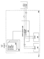
- the shared memory logic 104 is also coupled to a RAM (random access memory) 114 .
- data can be transferred from the RAM 114 for processing by the processing units 106 - 112 .
- transformed data e.g., encrypted or decrypted data
- the RAM 114 may represent a nexus between the component 100 and other system components (e.g., processor cores requesting cryptographic operations on data in RAM 114 ).
- the RAM 114 may be external to the die hosting the component 100 .
- FIG. 2 illustrates processing of a command to encrypt packet “A” stored in RAM 114 by a program executed by core 102 .
- another processor core may send the command to component 100 to prepare transmission of packet “A” across a public network.
- the sample program (1) reads the packet and any associated cryptography context (e.g., keys, initial vectors, or residue) into shared memory from RAM 114 ; (2) sends the data to an aligning processing unit 106 that writes the data back into shared memory 114 aligned on a specified byte boundary; (3) sends the data to a cipher processing unit 108 that performs a transformative cipher operation on the data before sending the transformed data to memory 104 ; and (4) transfers the transformed data to RAM 114 .
- the core 102 may then generate a signal or message notifying the processor core that issued the command that encryption is complete.
- the processor core 102 may be a multi-threaded processor core including storage for multiple program counters and contexts associated with multiple, respective, threads of program execution. That is, in FIG. 2 , thread 130 may be one of multiple threads.
- the core 102 may switch between thread contexts to mask latency associated with processing unit 106 - 112 operation.
- thread 130 may include an instruction (not shown) explicitly relinquishing thread 130 execution after an instruction sending data to the cipher processing unit 108 until receiving an indication that the transformed data has been written into shared memory 104 .
- the core 102 may use pre-emptive context switching that automatically switches contexts after certain events (e.g., requesting operation of a processing unit 106 - 112 or after a certain amount of execution time).
- Thread switching enables a different thread to perform other operations such as processing of a different packet in what would otherwise be wasted core 102 cycles. Throughput can be potentially be increased by adding additional contexts to the core 102 .
- threads can be assigned to commands in a variety of ways, for example, by a dispatcher thread that assigns threads to commands or by threads dequeuing commands when the threads are available.
- FIG. 3 illustrates a sample implementation of a processor 124 including a cryptographic system component 100 .
- the component 100 receives commands from processor core(s) 118 - 122 .
- core 102 is integrated into the system component 100 and services commands from the other cores 118 - 122 .
- processing core 102 may not be integrated within the component. Instead cores 118 - 122 may have direct control over component 100 operation. Alternately, one of cores 118 - 122 , may be designated for controlling the cryptographic component 100 and servicing requests received from the other cores 118 - 122 . This latter approach can lessen the expense and die footprint of the component 100 .
- the different processing units 106 - 112 may feature the same uniform interface architecture to the shared memory logic 104 .
- This uniformity eases the task of programming by making interaction with each processing unit very similar.
- the interface architecture also enables the set of processing units 106 - 112 included within the component 100 to be easily configured.
- a component 100 can be configured to include multiple copies of the same processing unit. For instance, if the component 100 is likely to be included in a system that will perform a large volume of authentication operations, the component 100 may be equipped with multiple hash processing units.
- the architecture enables new processing units to be easily integrated into the component 100 . For example, when a new cryptography algorithm emerges, a processing unit to implement the algorithm can be made available.
- each processing unit includes an input buffer 142 that receives data from shared memory logic 104 and an output buffer 140 that stores data to transfer to shared memory logic 104 .
- the processing unit 106 also includes processing logic 144 such as programmable or dedicated hardware (e.g., an Application Specific Integrated Circuit (ASIC)) to operate on data received by input buffer 142 and write operation results to buffer 140 .
- buffers 140 , 142 may include memory and logic (not shown) that queue data in the buffers based on the order in which data is received. For example, the logic may feature head and tail pointers into the memory and may append newly received data to the tail.
- a processing unit READ instruction causes a data push from shared memory to a respective target processing unit's 106 - 112 input buffer 142 via bus 146
- a processing unit WRITE instruction causes a data pull from a target processing unit's 106 - 112 output buffer 140 into shared memory via bus 148
- a core 102 program may issue a command to first push data to the processing unit and later issue a command to pull the results written into the processing unit's output buffer 144 .
- a wide variety of other inter-component 100 communication schemes may be used.
- FIG. 5 depicts shared memory logic 104 of the sample implementation.
- the logic 104 includes a READ queue and a WRITE queue for each processing unit (labeled “PU”).
- PU processing unit
- Commands to transfer data to/from the banks of shared memory (banks a-n) are received at an inlet queue 180 and sorted into the queues 170 - 171 based on the target processing unit and the type of command (e.g., READ or WRITE).
- the logic 104 also permits cores external to the component (e.g., cores 118 - 122 ) to READ (e.g., pull) or WRITE (e.g., push) data from/to the memory banks and features an additional pair of queues (labeled “cores”) for these commands.
- Arbiters 182 - 184 dequeue commands from the queues 170 - 171 .
- each arbiter 182 - 184 may use a round robin or other servicing scheme.
- the arbiters 182 - 184 forward the commands to another queue 172 - 178 based on the type of command.
- commands pushing data to an external core are enqueued in queue 176 while commands pulling data from an external core enqueued in queue 172 .
- commands pushing data to a processing unit are enqueued in queue 178 while commands pulling data from a processing unit are enqueued in queue 174 .
- the logic 104 initiates a transfer of data/to from the memory banks to the processing unit using buses 146 or 148 as appropriate or by sending/receiving data by a bus coupling the component 100 to the cores 118 - 122 .
- the logic 104 also includes circuitry to permit transfer (push and pulls) of data between the memory banks and the external RAM 114 .
- the processing units 150 - 154 can decompose a multiplication into a set of smaller partial products that can be more efficiently performed by the multiplier 156 .
- multiplication of two 1024-bit operands can be computed as four sets of 512-bit ⁇ 512 bit multiplications or sixteen sets of 256-bit ⁇ 256-bit multiplications.
- each processing unit 150 - 154 may feature an input buffer and an output buffer (see FIG. 4 ) to communicate with shared memory logic 104 .
- the multiplier 156 and processing units 150 - 154 may communicate using these buffers.
- a processing unit 150 - 154 may store operands to multiply in a pair of output queues in the output buffer for consumption by the multiplier 156 .
- the multiplier 156 results may be then transferred to the processing unit 150 - 154 upon completion.
- the same processing unit 150 - 154 input and output buffers may also be used to communicate with shared memory logic 104 .
- the input buffer of a processing unit 150 - 154 may receive program instructions and operands from shared memory logic 104 .
- the processing unit 150 - 154 may similarly store the results of program execution in an output buffer for transfer to the shared memory logic 104 upon completion of program execution.
- the processing units 150 - 154 provide multiple modes of operation that can be selected by program instructions executed by the processing units. For example, in “I/O” mode, the buffers of programming unit 150 - 154 exclusively exchange data with shared memory logic unit 104 via interface 158 . In “run” mode, the buffers of the unit 150 - 154 exclusively exchange data with multiplier 156 instead. Additional processing unit logic (not shown), may interact with the interface 158 and the multiplier 156 to indicate the processing unit's current mode.
- the arithmetic logic unit 216 is also coupled to and can operate on operands stored in input queue 220 (e.g., data transferred to the processing unit 150 , for example, from the multiplier or shared memory logic 104 ).
- the size of operands used by the arithmetic logic unit 216 to perform a given operation can vary and can be specified by program instructions.
- the components described above form a cyclic datapath. That is, operands flow from the input buffer 220 , data banks 212 , 214 through the arithmetic logic unit 216 and either back into the data banks 212 , 214 or to the output buffer(s) 222 . Operation of the datapath is controlled by program instructions stored in control store 204 and executed by control logic 206 .
- the control logic 206 has a store of global variables 208 and a set of variable references 202 (e.g., pointers) into data stored in data banks 212 , 214 .
- control logic 206 includes instructions (“setup” instructions) to assign variable values, instructions (“exec” and “fexec” instructions) to perform mathematical and logical operations, and control flow instructions such as procedure calls and conditional branching instructions.
- the processing unit 150 provides a set of user accessible bits that can be used as conditions for conditional instructions.
- FIG. 11 depicts sample operation of an “FEXEC” (FIFO EXEC) instruction that combines aspects of the FIFO and EXEC instructions.
- FEXEC FIFO EXEC
- an FEXEC instruction supplies operands to the arithmetic logic unit 216 .
- an operand can be supplied from the input queue 222 .
- control logic 206 may execute other instructions concurrently with operations caused by datapath instructions.
- control logic 206 may execute control flow logic instructions (e.g., a conditional branch) and variable assignment instructions before previously initiated datapath operations complete.
- control flow logic instructions e.g., a conditional branch
- FIFO instructions may issue concurrently with any branch instruction or any setup instruction except a mode instruction.
- FIFO instructions may issue concurrently with any execute instruction provided the destination banks for both are mutually exclusive.
- FEXEC and EXEC instructions may issue concurrently with any mode instructions and instructions that do not rely on the existence of particular condition states. EXEC instructions, however, may not issue concurrently with FEXEC instructions.
- the processing unit 150 provides a number of features that can ease the task of programming cryptographic operations. For example, programs implementing many algorithms can benefit from recursion or other nested execution of subroutines or functions. As shown in FIG. 13 , the processing unit may maintain different scopes 250 - 256 of variables and conditions that correspond to different depths of nested subroutine/function execution.
- the control logic uses one of the scopes 250 - 256 as the current scope. For example, the current scope in FIG. 13 is scope 252 . While a program executes, the variable and condition values specified by this scope are used by the control logic 206 . For example, a reference to variable “A0” by an instruction would be associated with A0 of the current scope 252 .
- the control logic 206 can automatically increment or decrement the scope index in response to procedure calls (e.g., subroutine calls, function calls, or method invocations) and procedure exits (e.g., returns), respectively.
- procedure calls e.g., subroutine calls, function calls, or method invocations
- procedure exits e.g., returns
- the processing unit instruction set also provides instructions (e.g., “set scope ⁇ target scope>”) that provide explicit access to scope variables in a target scope other than the current scope.
- a program may initially setup, in advance, the diminishing scales associated with an ensuing set of recursive/nested subroutine calls.
- the instruction set includes an instruction to set each of the scope fields.
- the instruction set includes an instruction (e.g., “copy_scope”) to copy an entire set of scope values from the current scope to a target scope.
- the instruction set includes instructions to permit scope values to be computed based on the values included in a different scope (e.g., “set variable relative”).
- the processing unit 150 also can include logic to reduce the burden of exponentiation.
- many cryptographic operations require exponentiation of large numbers.
- FIG. 14 depicts an exponent 254 raising some number, g, to the 6,015,455,113-th power.
- many algorithms reduce the operation to a series of simpler mathematical operations.
- an algorithm can process the exponent 254 as a bit string and proceeding bit-by-bit from left to right (most-significant-bit to least-significant-bit). For example, starting with an initial value of “1”, the algorithm can square the value for each “0” encountered in the bit string. For each “1” encountered in the bit string, the algorithm can square the value and multiply by g. For example, to determine the value of 2 ⁇ 9, the algorithm would operate on the binary exponent of 1001b as follows:
- an exponent can be searched for windows of bits that correspond to pre-computed values. For example, in the trivially small example of 2 ⁇ 9, a bit pattern of “10” corresponds to g ⁇ 2 (4). Thus, identifying the “10” window value in exponent “1001” enables the algorithm to simply square the value for each bit within the window and multiply by the precomputed value. Thus, an algorithm using windows could proceed:
- an exponent window of “1011” is found at location 256 a and an exponent window of “1101” is found at location 256 b .
- the window bits are zeroed. For example, as shown, a window of “0011” is found at location 256 c . Zeroing the exponent bits enables a window of “0001” to be found at location 256 d.
- the greater swath of bits included in the search permits the logic 250 to select from different potential windows found within the M-bits (e.g., windows with the most number of “1” bits). For example, in FIG. 14 , the exponent 254 begins with bits of “0001”, however this potential window is not selected in favor of the window “1011” using “look-ahead” bits (C ⁇ 1-C ⁇ 4).
- the logic 210 can output a “window found” signal identifying the index of the window within the exponent string.
- the logic 210 can also output the pattern of non-zero bits found. This pattern can be used as a lookup key into a table of pre-computed window values. Finally, the logic 210 zeroes the bits within the window and continues to search for window-sized bit-patterns.
- the logic 210 shown can be included in a processing unit.
- FIG. 7 depicts the logic 210 as receiving the output of shifter 218 which rotates bits of an exponent through the logic 210 .
- the logic 210 is also coupled to control logic 206 .
- the control logic 206 can feature instructions that control operation of the windowing logic (e.g., to set the window size and/or select fixed or sliding window operation) and to respond to logic 210 output.
- the control logic 206 can include a conditional branching instruction that operates on “window found” output of the control logic.
- a program can branch on a window found condition and use the output index to lookup a precomputed value for the window.
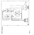
- FIG. 16 illustrates sample operation of a multiplier implementation.
- the multiplier 156 operates on two operands, A 256 and B 258 , over a series of clock cycles.
- the operands are handled by the multiplier as sets of segments, though the number of segments and/or the segment size for each operand differs. For instance, in the example shown, the N-bits of operand A are divided into 8-segments (0-7) while operand B is divided into 2-segments (0-1).
- multiplication of the least significant segments of A and B (B0 ⁇ A0) 262 a results in the least significant set of resulting bits with multiplication of the most significant segments of A and B (B1 ⁇ A7) 262 l results in the most significant set of resulting bits.
- the addition of the results of the series of partial products represents the multiplication of operands A 256 and B 258 .
- Sequencing computation of the series of partial products can incrementally yields bits of the final multiplication result well before the final cycle.
- FIG. 16 identifies when bits of a given significance can be retired as arrowed lines spanning the bits. For example, after completing B0 ⁇ A0 in cycle 2, the least significant bits of the final result are known since subsequent partial product results do not affect these bits. Similarly, after completing B0 ⁇ A1 in cycle 3, bits can be retired since only partial products 262 a and 262 b affect the sum of these least significant bits. As shown, each cycle may not result in bits being retired. For example multiplication of different segments can yields bits occupying the exact same significance. For example, the results of B0 ⁇ A4 in cycle 6 and B1 ⁇ A0 in cycle 7 exactly overlap. Thus, no bits are retired in cycle 6.
- the multipliers 156 are supplied segments of the operands in turn, for example, as shown in FIG. 16 .
- segment 0 of operand A is supplied to each multiplier 306 - 312 while sub-segments d-a of segment 0 of operand B are respectively supplied to each multiplier 306 - 312 .
- multiplier 312 may receive segment 0 of operand A and segment 0, sub-segment a of operand B while multiplier 310 receives segment 0 of operand A and segment 0, sub-segment, b of operand B in a given cycle.
- the outputs of the multipliers 306 - 312 are shifted 314 - 318 based on the significance of the respective segments within the operands. For example, shifter 318 shifts the results of Bnb ⁇ An 314 with respect to the results of Bna ⁇ An 312 to reflect the significance of sub-segment b relative to sub-segment a.
- sequencing of the segment multiplications can result in the output of bits by the multipliers 306 - 312 that are not affected by subsequent output by the multipliers 306 - 312 .
- the least significant bits output by the multipliers 306 - 312 can sent to the accumulator 320 in cycle-2.
- the accumulator 320 can retire such bits as they are produced.
- the accumulator 320 can output retired bits to a pair of FIFOs 322 , 324 that store the accumulated carry/save vectors respectively.
- the FIFOs 322 , 324 store bits of the carry/save vectors retired by the accumulator 320 .
- the FIFOs 322 , 324 feed an adder 330 that sums the retired portions of carry/save vectors.
- the FIFOs 322 , 324 can operate to smooth feeding of bits to the adder 330 such that the adder 330 is continuously fed retired portions in each successive cycle until the final multiplier result is output. In other words, as shown in FIG. 16 , not all cycles (e.g., cycle-6) result in retiring bits. Without FIFOs 322 , 324 , the adder 330 would stall when these cycles-without-retirement filter down through the multiplier 156 .
- the FIFOs 322 , 324 can ensure continuous operation of the adder 330 .
- the FIFOs 322 , 324 need not be as large as the number of bits in the final multiplier 156 result. Instead the FIFOs 322 , 324 may only be large enough to store a sufficient number of retired bits such that “skipped” retirement cycles do stall the adder 330 and large enough to accommodate the burst of retired bits in the final cycles.
- the multiplier 156 acts as a pipeline that propagates data through the multiplier stages in a series of cycles. As shown the multiplier features two queues 302 , 304 that store operands to be multiplied. To support the partial product multiplication scheme described above, the width of the queues 302 , 304 may vary with each queue being the width of 1-operand-segment. The queues 302 , 304 prevent starvation of the pipeline. That is, as the multipliers complete multiplication of one pair of operands, the start of the multiplication of another pair of operands can immediately follow.
- logic 326 , 328 can zero the accumulator 320 vectors to start multiplication of two new dequeued operands.
- the multiplication of two operands may begin before the multiplier receives the entire set of segments in the operands.
- the multiplier may begin A ⁇ B as soon as segments A0 and B0 are received.
- the FIFOs 322 , 324 can not only smooth output of the adder 330 for a given pair of operands but can also smooth output of the adder 330 across different sets of operands.
- the multiplier 156 may output portions of the final multiplication results for multiple multiplication problems with each successive cycle. That is, after the cycle outputting the most significant bits of A ⁇ B, the least significant bits of C ⁇ D are output.
- the multiplier 156 can obtain operands, for example, by receiving data from the processing unit output buffers. To determine which processing unit to service, the multiplier may feature an arbiter (not shown). For example, the arbiter may poll each processing unit in turn to determine whether a given processing unit has a multiplication to perform. To ensure multiplier 156 cycles are not wasted, the arbiter may determine whether a given processing unit has enqueued a sufficient amount of the operands and whether the processing unit has sufficient space in its input buffer to hold the results before selecting the processing unit for service.
- an arbiter not shown
- the arbiter may poll each processing unit in turn to determine whether a given processing unit has a multiplication to perform.
- the arbiter may determine whether a given processing unit has enqueued a sufficient amount of the operands and whether the processing unit has sufficient space in its input buffer to hold the results before selecting the processing unit for service.
- a given processing unit may decompose a given algorithm into a series of multiplications.
- the arbiter may detect a signal provided by the processing unit that signals the arbiter to continue servicing additional sets of operands provided by the processing unit currently being serviced by the multiplier. In the absence of such a signal, the arbiter resumes servicing of the other processing units for example by resuming round-robin polling of the processing units.
- FIG. 19 depicts an example of an authentication/hash processing unit.
- the unit stores data (“common authentication data structures”) that are used for message authentication that are shared among the different authentication algorithms (e.g., configuration and state registers).
- the unit also includes dedicated hardware logic responsible for the data processing for each algorithm supported (e.g., MD5 logic, SHA logic, AES logic, and Kasumi logic).
- the overall operation of the unit is controlled by control logic and a finite state machine (FSM).
- the FSM controls the loading and unloading of data in the authentication data buffer, tracks the amount of data in the data buffer, sends a start signal to the appropriate authentication core, controls the source of data that gets loaded into the data buffer, and sends information to padding logic to help determine padding data.
- FSM finite state machine
- the unit also includes control logic and a state machine.
- the logic block is responsible for controlling the overall behavior of the cipher unit including enabling the appropriate datapath depending on the mode the cipher unit is in (e.g., in encryption CBC mode, the appropriate IV is chosen to generate the encrypt IV while the decrypt IV is set to 0), selecting the appropriate inputs into the cipher cores throughout the duration of cipher processing (e.g., the IV, the counter, and the key to be used), and generating control signals that determine what data to send to the output datapath based on the command issued by the core 102 .
- This block also initiates and generates the necessary control signals for RC4 key expansion and AES key conversion.
- the processing units shown in FIGS. 18-20 are merely examples of different types of processing units and the component may feature many different types of units other than those shown.
- the component may include a unit to perform pseudo random number generation, a unit to perform Reed-Solomon coding, and so forth.
- FIG. 21 depicts an example of network processor 400 that can be programmed to process packets.
- the network processor 400 shown is an Intel® Internet eXchange network Processor (IXP).
- IXP Internet eXchange network Processor
- Other processors feature different designs.
- the network processor 400 shown features a collection of programmable processing cores 402 on a single integrated semiconductor die 400 .
- Each core 402 may be a Reduced Instruction Set Computer (RISC) processor tailored for packet processing.
- RISC Reduced Instruction Set Computer
- the cores 402 may not provide floating point or integer division instructions commonly provided by the instruction sets of general purpose processors.
- Individual cores 402 may provide multiple threads of execution.
- a core 402 may store multiple program counters and other context data for different threads.
- the network processor 400 also features an interface 420 that can carry packets between the processor 400 and other network components.
- the processor 400 can feature a switch fabric interface 420 (e.g., a Common Switch Interface (CSIX)) that enables the processor 400 to transmit a packet to other processor(s) or circuitry connected to a switch fabric.
- the processor 400 can also feature an interface 420 (e.g., a System Packet Interface (SPI) interface) that enables the processor 400 to communicate with physical layer (PHY) and/or link layer devices (e.g., MAC or framer devices).
- the processor 400 may also include an interface 404 (e.g., a Peripheral Component Interconnect (PCI) bus interface) for communicating, for example, with a host or other network processors.
- PCI Peripheral Component Interconnect
- the processor 400 includes other resources shared by the cores 402 such as the cryptography component 100 , internal scratchpad memory, and memory controllers 416 , 418 that provide access to external memory.
- the network processor 400 also includes a general purpose processor 406 (e.g., a StrongARM® XScale® or Intel Architecture core) that is often programmed to perform “control plane” or “slow path” tasks involved in network operations while the cores 402 are often programmed to perform “data plane” or “fast path” tasks.
- a general purpose processor 406 e.g., a StrongARM® XScale® or Intel Architecture core
- the cores 402 may communicate with other cores 402 via the shared resources (e.g., by writing data to external memory or the scratchpad 408 ).
- the cores 402 may also intercommunicate via neighbor registers directly wired to adjacent core(s) 402 .
- the cores 402 may also communicate via a CAP (CSR (Control Status Register) Access Proxy) 410 unit that routes data between cores 402 .
- CSR Control Status Register
- FIG. 22 depicts a sample core 402 in greater detail.
- the core 402 architecture shown in FIG. 22 may also be used in implementing the core 102 shown in FIG. 1 .
- the core 402 includes an instruction store 512 to store program instructions.
- the core 402 may include an ALU (Arithmetic Logic Unit), Content Addressable Memory (CAM), shifter, and/or other hardware to perform other operations.
- the core 402 includes a variety of memory resources such as local memory 502 and general purpose registers 504 .
- the core 402 shown also includes read and write transfer registers 508 , 510 that store information being sent to/received from targets external to the core.
- the core 402 also includes next neighbor registers 506 , 516 that store information being directly sent to/received from other cores 402 .
- the data stored in the different memory resources may be used as operands in the instructions.
- the core 402 also includes a commands queue 524 that buffers commands (e.g., memory access commands) being sent to targets external to the core.
- threads executing on the core 402 may send commands via the commands queue 524 . These commands may identify transfer registers within the core 402 as the destination for command results (e.g., a completion message and/or the location of encrypted data in memory).
- the core 402 may feature an instruction set to reduce idle core cycles while waiting, for example for completion of a request by the cryptography component 100 .
- the core 402 may provide a ctx_arb (context arbitration) instruction that enables a thread to swap out of execution until receiving a signal associated with component 100 completion of an operation.
- FIG. 23 depicts a network device that can process packets using a cryptography component.
- the device features a collection of blades 608 - 620 holding integrated circuitry interconnected by a switch fabric 610 (e.g., a crossbar or shared memory switch fabric).
- a switch fabric 610 e.g., a crossbar or shared memory switch fabric.
- the device features a variety of blades performing different operations such as I/O blades 608 a - 608 n , data plane switch blades 618 a - 618 b , trunk blades 612 a - 612 b , control plane blades 614 a - 614 n , and service blades.
- the switch fabric may conform to CSIX or other fabric technologies such as HyperTransport, Infiniband, PCI, Packet-Over-SONET, RapidIO, and/or UTOPIA (Universal Test and Operations PHY Interface for ATM).
- Individual blades may include one or more physical layer (PHY) devices (not shown) (e.g., optic, wire, and wireless PHYs) that handle communication over network connections.
- PHY physical layer
- the PHYs translate between the physical signals carried by different network mediums and the bits (e.g., “0”-s and “1”-s) used by digital systems.
- the line cards 608 - 620 may also include framer devices (e.g., Ethernet, Synchronous Optic Network (SONET), High-Level Data Link (HDLC) framers or other “layer 2” devices) 602 that can perform operations on frames such as error detection and/or correction.
- framer devices e.g., Ethernet, Synchronous Optic Network (SONET), High-Level Data Link (HDLC) framers or other “layer 2” devices
- the blades 608 a shown may also include one or more network processors 604 , 606 that perform packet processing operations for packets received via the PHY(s) 602 and direct the packets, via the switch fabric 610 , to a blade providing an egress interface to forward the packet. Potentially, the network processor(s) 606 may perform “layer 2” duties instead of the framer devices 602 .
- the network processors 604 , 606 may feature techniques described above.
- FIGS. 21-23 described specific examples of a network processor and a device incorporating network processors
- the techniques may be implemented in a variety of architectures including general purpose processors, network processors and network devices having designs other than those shown. Additionally, the techniques may be used in a wide variety of network devices (e.g., a router, switch, bridge, hub, traffic generator, and so forth). Further, many of the techniques described above may be found in components other than components to perform cryptographic operations.
- circuitry as used herein includes hardwired circuitry, digital circuitry, analog circuitry, programmable circuitry, and so forth.
- the programmable circuitry may operate on computer programs disposed on a computer readable medium.
- This appendix contains material which is subject to copyright protection.
- Output Queue B - can be enqueued with data from the output of the ALU or from the variable specified in operand 1 (Bank B).
- (‘—’ indicates that there is no data enqueued to Output Queue B)
- Operand 2 of the second control word specifies the index of the destination variable in the current scope to be written and write bank determines which is the relevant bank.
- Bits Name Description 8 A/B Bank select 0 - Bank A 1 - Bank B 7:6 Dest Destination Variable Number - index of a target scope variable 5:4 Src Source Variable Number - index of a current scope variable 3:1 Scale Scale as defined by the operand definition in the execute command.
- 0 I/W Index/Window flag defines the offset to be either the index in the current scope or the appropriate bits from the windowing hardware.
- 0 - Index the offset is specified by the index of the current scope 1 - Window: the offset is specified by the upper ⁇ C 1 , . . .
- Src Source - selects the source of the target scope 00 - the Immed field 01 - the (3 lsbs of) global variable defined the Global field 10 - an increment or decrement (defined by the I/D field) of the current target scope (hardware will allow wrap-around of scope values) 11 - the current scope plus one 6:4 Immed Immediate value - index of a scope in the variable ram 3:2 Global Global variable - index of a global variable 1 I/D Increment/Decrement flag 0 - Increment the target scope 1 - Decrement the target scope
Landscapes
- Physics & Mathematics (AREA)
- Engineering & Computer Science (AREA)
- General Physics & Mathematics (AREA)
- Mathematical Analysis (AREA)
- Mathematical Optimization (AREA)
- Pure & Applied Mathematics (AREA)
- Computational Mathematics (AREA)
- Theoretical Computer Science (AREA)
- Computing Systems (AREA)
- General Engineering & Computer Science (AREA)
- Advance Control (AREA)
- Complex Calculations (AREA)
- Magnetic Resonance Imaging Apparatus (AREA)
- Holo Graphy (AREA)
Priority Applications (7)
| Application Number | Priority Date | Filing Date | Title |
|---|---|---|---|
| US11/323,994 US8073892B2 (en) | 2005-12-30 | 2005-12-30 | Cryptographic system, method and multiplier |
| DE602006017589T DE602006017589D1 (de) | 2005-12-30 | 2006-12-18 | Multiplikator |
| AT06845803T ATE484789T1 (de) | 2005-12-30 | 2006-12-18 | Multiplikator |
| EP06845803A EP1966680B1 (de) | 2005-12-30 | 2006-12-18 | Multiplikator |
| PCT/US2006/048417 WO2007078939A2 (en) | 2005-12-30 | 2006-12-18 | Multiplier |
| CNA2006100642259A CN101149675A (zh) | 2005-12-30 | 2006-12-29 | 乘法器 |
| CNA2006101309997A CN101042639A (zh) | 2005-12-30 | 2006-12-30 | 乘法器 |
Applications Claiming Priority (1)
| Application Number | Priority Date | Filing Date | Title |
|---|---|---|---|
| US11/323,994 US8073892B2 (en) | 2005-12-30 | 2005-12-30 | Cryptographic system, method and multiplier |
Publications (2)
| Publication Number | Publication Date |
|---|---|
| US20110264720A1 US20110264720A1 (en) | 2011-10-27 |
| US8073892B2 true US8073892B2 (en) | 2011-12-06 |
Family
ID=38093399
Family Applications (1)
| Application Number | Title | Priority Date | Filing Date |
|---|---|---|---|
| US11/323,994 Expired - Fee Related US8073892B2 (en) | 2005-12-30 | 2005-12-30 | Cryptographic system, method and multiplier |
Country Status (6)
| Country | Link |
|---|---|
| US (1) | US8073892B2 (de) |
| EP (1) | EP1966680B1 (de) |
| CN (2) | CN101149675A (de) |
| AT (1) | ATE484789T1 (de) |
| DE (1) | DE602006017589D1 (de) |
| WO (1) | WO2007078939A2 (de) |
Cited By (11)
| Publication number | Priority date | Publication date | Assignee | Title |
|---|---|---|---|---|
| US20130030916A1 (en) * | 2011-07-25 | 2013-01-31 | Brandverity, Inc. | Affiliate investigation system and method |
| US8924741B2 (en) | 2012-12-29 | 2014-12-30 | Intel Corporation | Instruction and logic to provide SIMD secure hashing round slice functionality |
| US9027104B2 (en) | 2012-12-28 | 2015-05-05 | Intel Corporation | Instructions processors, methods, and systems to process secure hash algorithms |
| US9912481B2 (en) | 2014-03-27 | 2018-03-06 | Intel Corporation | Method and apparatus for efficiently executing hash operations |
| US10038550B2 (en) | 2013-08-08 | 2018-07-31 | Intel Corporation | Instruction and logic to provide a secure cipher hash round functionality |
| US20190057050A1 (en) * | 2018-10-15 | 2019-02-21 | Amrita MATHURIYA | Pipeline circuit architecture to provide in-memory computation functionality |
| US10503510B2 (en) | 2013-12-27 | 2019-12-10 | Intel Corporation | SM3 hash function message expansion processors, methods, systems, and instructions |
| US10592245B2 (en) | 2014-09-26 | 2020-03-17 | Intel Corporation | Instructions and logic to provide SIMD SM3 cryptographic hashing functionality |
| US10623175B2 (en) | 2014-09-04 | 2020-04-14 | Intel Corporation | SM3 hash algorithm acceleration processors, methods, systems, and instructions |
| US10649774B2 (en) | 2009-12-22 | 2020-05-12 | Intel Corporation | Multiplication instruction for which execution completes without writing a carry flag |
| US12621126B2 (en) | 2024-09-18 | 2026-05-05 | Intel Corporation | SM3 hash algorithm acceleration processors, methods, systems, and instructions |
Families Citing this family (18)
| Publication number | Priority date | Publication date | Assignee | Title |
|---|---|---|---|---|
| US8073892B2 (en) | 2005-12-30 | 2011-12-06 | Intel Corporation | Cryptographic system, method and multiplier |
| US9191211B2 (en) * | 2009-02-27 | 2015-11-17 | Atmel Corporation | Data security system |
| US8654970B2 (en) * | 2009-03-31 | 2014-02-18 | Oracle America, Inc. | Apparatus and method for implementing instruction support for the data encryption standard (DES) algorithm |
| US20100250965A1 (en) * | 2009-03-31 | 2010-09-30 | Olson Christopher H | Apparatus and method for implementing instruction support for the advanced encryption standard (aes) algorithm |
| US8832464B2 (en) * | 2009-03-31 | 2014-09-09 | Oracle America, Inc. | Processor and method for implementing instruction support for hash algorithms |
| US9317286B2 (en) * | 2009-03-31 | 2016-04-19 | Oracle America, Inc. | Apparatus and method for implementing instruction support for the camellia cipher algorithm |
| US20100246815A1 (en) * | 2009-03-31 | 2010-09-30 | Olson Christopher H | Apparatus and method for implementing instruction support for the kasumi cipher algorithm |
| US9207941B2 (en) * | 2013-03-15 | 2015-12-08 | Intel Corporation | Systems, apparatuses, and methods for reducing the number of short integer multiplications |
| CN104239279A (zh) * | 2014-09-10 | 2014-12-24 | 哈尔滨工业大学深圳研究生院 | 一种乘法器 |
| GB2539881B (en) * | 2015-06-24 | 2018-07-25 | Advanced Risc Mach Ltd | An apparatus and method for processing floating point values |
| CN107861709B (zh) * | 2017-12-01 | 2021-04-02 | 中国兵器装备集团自动化研究所 | 适应前端高速处理的累加器和功率谱累加器及其累加方法 |
| US11599334B2 (en) * | 2020-06-09 | 2023-03-07 | VeriSilicon Microelectronics | Enhanced multiply accumulate device for neural networks |
| US20220171604A1 (en) * | 2020-12-02 | 2022-06-02 | Flex Logix Technologies, Inc. | Multiplier Circuit Array, MAC and MAC Pipeline including Same, and Methods of Configuring Same |
| WO2022191859A1 (en) * | 2021-03-12 | 2022-09-15 | Zeku, Inc. | Vector processing using vector-specific data type |
| CN113946846B (zh) * | 2021-10-14 | 2022-07-12 | 深圳致星科技有限公司 | 用于联邦学习和隐私计算的密文计算装置及方法 |
| CN117149129B (zh) * | 2023-10-31 | 2024-01-26 | 共模半导体技术(苏州)有限公司 | 专用大整数乘法微控制器 |
| CN117850736B (zh) * | 2024-03-06 | 2024-05-31 | 北京壁仞科技开发有限公司 | 乘法电路模块与乘法运算方法 |
| CN118917387A (zh) * | 2024-09-30 | 2024-11-08 | 国网北京市电力公司 | 联邦学习的加速方法、装置和非易失性存储介质 |
Citations (33)
| Publication number | Priority date | Publication date | Assignee | Title |
|---|---|---|---|---|
| US3515344A (en) * | 1966-08-31 | 1970-06-02 | Ibm | Apparatus for accumulating the sum of a plurality of operands |
| US4546446A (en) * | 1981-02-25 | 1985-10-08 | Nippon Electric Co., Ltd. | Digital processing circuit having a multiplication function |
| US4594679A (en) * | 1983-07-21 | 1986-06-10 | International Business Machines Corporation | High speed hardware multiplier for fixed floating point operands |
| US4775951A (en) * | 1982-12-20 | 1988-10-04 | Computer Basic Technology Research Association | Correlation function computing device |
| US4811269A (en) | 1985-10-09 | 1989-03-07 | Hitachi, Ltd. | Bit slice multiplication circuit |
| US5073870A (en) * | 1989-01-30 | 1991-12-17 | Nippon Telegraph And Telephone Corporation | Modular multiplication method and the system for processing data |
| JPH04216126A (ja) | 1990-12-14 | 1992-08-06 | Fujitsu Ltd | 直並列型乗算器 |
| US5150322A (en) * | 1990-06-05 | 1992-09-22 | Vlsi Technology, Inc. | Mixed-radix serial/parallel multipliers |
| US5524090A (en) * | 1992-06-25 | 1996-06-04 | Canon Kabushiki Kaisha | Apparatus for multiplying long integers |
| US5892699A (en) * | 1997-09-16 | 1999-04-06 | Integrated Device Technology, Inc. | Method and apparatus for optimizing dependent operand flow within a multiplier using recoding logic |
| US6035316A (en) * | 1995-08-31 | 2000-03-07 | Intel Corporation | Apparatus for performing multiply-add operations on packed data |
| US6182233B1 (en) * | 1998-11-20 | 2001-01-30 | International Business Machines Corporation | Interlocked pipelined CMOS |
| US20030065699A1 (en) * | 2001-10-01 | 2003-04-03 | Koninklijke Philips Electronics N.V. | Split multiplier for efficient mixed-precision DSP |
| CN1410880A (zh) | 2001-09-27 | 2003-04-16 | 中国科学院计算技术研究所 | 提高半规模双精度浮点乘法流水线效率的结构 |
| US6711602B1 (en) * | 2000-02-18 | 2004-03-23 | Texas Instruments Incorporated | Data processor with flexible multiply unit |
| US20050138366A1 (en) | 2003-12-19 | 2005-06-23 | Pan-Loong Loh | IPSec acceleration using multiple micro engines |
| US20050138368A1 (en) | 2003-12-19 | 2005-06-23 | Sydir Jaroslaw J. | Method and apparatus for performing an authentication after cipher operation in a network processor |
| US20050141715A1 (en) | 2003-12-29 | 2005-06-30 | Sydir Jaroslaw J. | Method and apparatus for scheduling the processing of commands for execution by cryptographic algorithm cores in a programmable network processor |
| US20050144211A1 (en) * | 2003-12-29 | 2005-06-30 | Xilinx, Inc. | Programmable logic device with pipelined DSP slices |
| US20050149725A1 (en) | 2003-12-30 | 2005-07-07 | Intel Corporation | Method and apparatus for aligning ciphered data |
| US20050149744A1 (en) | 2003-12-29 | 2005-07-07 | Intel Corporation | Network processor having cryptographic processing including an authentication buffer |
| US20050154960A1 (en) | 2003-12-30 | 2005-07-14 | Sydir Jaroslaw J. | Method and apparatus for calculating CRC on data using a programmable CRC engine |
| US20050198093A1 (en) * | 2004-03-02 | 2005-09-08 | Hee-Kwan Son | Montgomery modular multiplier |
| US20050238166A1 (en) | 2004-04-27 | 2005-10-27 | Koshy Kamal J | Apparatus and method for implementing the KASUMI ciphering process |
| US20050240764A1 (en) | 2004-04-27 | 2005-10-27 | Koshy Kamal J | Apparatus and method for performing RC4 ciphering |
| US20060010327A1 (en) | 2004-06-25 | 2006-01-12 | Koshy Kamal J | Apparatus and method for performing MD5 digesting |
| US20060059219A1 (en) | 2004-09-16 | 2006-03-16 | Koshy Kamal J | Method and apparatus for performing modular exponentiations |
| US20060059220A1 (en) | 2004-09-16 | 2006-03-16 | Koshy Kamal J | Method and apparatus for performing montgomery multiplications |
| US20070061392A1 (en) * | 2005-09-09 | 2007-03-15 | International Business Machines Corp. | Fused multiply add split for multiple precision arithmetic |
| WO2007078939A2 (en) | 2005-12-30 | 2007-07-12 | Intel Corporation | Multiplier |
| US7266580B2 (en) * | 2003-05-12 | 2007-09-04 | International Business Machines Corporation | Modular binary multiplier for signed and unsigned operands of variable widths |
| US7373368B1 (en) * | 2003-01-30 | 2008-05-13 | Sun Microsystems, Inc. | Multiply execution unit that includes 4:2 and/or 5:3 compressors for performing integer and XOR multiplication |
| US20090037508A1 (en) * | 2005-04-01 | 2009-02-05 | Florent Bernard | Method for implementing montgomery modular multiplication and device therefore |
-
2005
- 2005-12-30 US US11/323,994 patent/US8073892B2/en not_active Expired - Fee Related
-
2006
- 2006-12-18 DE DE602006017589T patent/DE602006017589D1/de active Active
- 2006-12-18 EP EP06845803A patent/EP1966680B1/de not_active Not-in-force
- 2006-12-18 AT AT06845803T patent/ATE484789T1/de not_active IP Right Cessation
- 2006-12-18 WO PCT/US2006/048417 patent/WO2007078939A2/en not_active Ceased
- 2006-12-29 CN CNA2006100642259A patent/CN101149675A/zh active Pending
- 2006-12-30 CN CNA2006101309997A patent/CN101042639A/zh active Pending
Patent Citations (34)
| Publication number | Priority date | Publication date | Assignee | Title |
|---|---|---|---|---|
| US3515344A (en) * | 1966-08-31 | 1970-06-02 | Ibm | Apparatus for accumulating the sum of a plurality of operands |
| US4546446A (en) * | 1981-02-25 | 1985-10-08 | Nippon Electric Co., Ltd. | Digital processing circuit having a multiplication function |
| US4775951A (en) * | 1982-12-20 | 1988-10-04 | Computer Basic Technology Research Association | Correlation function computing device |
| US4594679A (en) * | 1983-07-21 | 1986-06-10 | International Business Machines Corporation | High speed hardware multiplier for fixed floating point operands |
| US4811269A (en) | 1985-10-09 | 1989-03-07 | Hitachi, Ltd. | Bit slice multiplication circuit |
| US5073870A (en) * | 1989-01-30 | 1991-12-17 | Nippon Telegraph And Telephone Corporation | Modular multiplication method and the system for processing data |
| US5150322A (en) * | 1990-06-05 | 1992-09-22 | Vlsi Technology, Inc. | Mixed-radix serial/parallel multipliers |
| JPH04216126A (ja) | 1990-12-14 | 1992-08-06 | Fujitsu Ltd | 直並列型乗算器 |
| US5524090A (en) * | 1992-06-25 | 1996-06-04 | Canon Kabushiki Kaisha | Apparatus for multiplying long integers |
| US6035316A (en) * | 1995-08-31 | 2000-03-07 | Intel Corporation | Apparatus for performing multiply-add operations on packed data |
| US5892699A (en) * | 1997-09-16 | 1999-04-06 | Integrated Device Technology, Inc. | Method and apparatus for optimizing dependent operand flow within a multiplier using recoding logic |
| US6182233B1 (en) * | 1998-11-20 | 2001-01-30 | International Business Machines Corporation | Interlocked pipelined CMOS |
| US6711602B1 (en) * | 2000-02-18 | 2004-03-23 | Texas Instruments Incorporated | Data processor with flexible multiply unit |
| CN1410880A (zh) | 2001-09-27 | 2003-04-16 | 中国科学院计算技术研究所 | 提高半规模双精度浮点乘法流水线效率的结构 |
| US20030065699A1 (en) * | 2001-10-01 | 2003-04-03 | Koninklijke Philips Electronics N.V. | Split multiplier for efficient mixed-precision DSP |
| US7373368B1 (en) * | 2003-01-30 | 2008-05-13 | Sun Microsystems, Inc. | Multiply execution unit that includes 4:2 and/or 5:3 compressors for performing integer and XOR multiplication |
| US7266580B2 (en) * | 2003-05-12 | 2007-09-04 | International Business Machines Corporation | Modular binary multiplier for signed and unsigned operands of variable widths |
| US20050138368A1 (en) | 2003-12-19 | 2005-06-23 | Sydir Jaroslaw J. | Method and apparatus for performing an authentication after cipher operation in a network processor |
| US20050138366A1 (en) | 2003-12-19 | 2005-06-23 | Pan-Loong Loh | IPSec acceleration using multiple micro engines |
| US20050141715A1 (en) | 2003-12-29 | 2005-06-30 | Sydir Jaroslaw J. | Method and apparatus for scheduling the processing of commands for execution by cryptographic algorithm cores in a programmable network processor |
| US20050149744A1 (en) | 2003-12-29 | 2005-07-07 | Intel Corporation | Network processor having cryptographic processing including an authentication buffer |
| US20050144211A1 (en) * | 2003-12-29 | 2005-06-30 | Xilinx, Inc. | Programmable logic device with pipelined DSP slices |
| US20050149725A1 (en) | 2003-12-30 | 2005-07-07 | Intel Corporation | Method and apparatus for aligning ciphered data |
| US20050154960A1 (en) | 2003-12-30 | 2005-07-14 | Sydir Jaroslaw J. | Method and apparatus for calculating CRC on data using a programmable CRC engine |
| US20050198093A1 (en) * | 2004-03-02 | 2005-09-08 | Hee-Kwan Son | Montgomery modular multiplier |
| US20050240764A1 (en) | 2004-04-27 | 2005-10-27 | Koshy Kamal J | Apparatus and method for performing RC4 ciphering |
| US20050238166A1 (en) | 2004-04-27 | 2005-10-27 | Koshy Kamal J | Apparatus and method for implementing the KASUMI ciphering process |
| US20060010327A1 (en) | 2004-06-25 | 2006-01-12 | Koshy Kamal J | Apparatus and method for performing MD5 digesting |
| US20060059219A1 (en) | 2004-09-16 | 2006-03-16 | Koshy Kamal J | Method and apparatus for performing modular exponentiations |
| US20060059220A1 (en) | 2004-09-16 | 2006-03-16 | Koshy Kamal J | Method and apparatus for performing montgomery multiplications |
| US20090037508A1 (en) * | 2005-04-01 | 2009-02-05 | Florent Bernard | Method for implementing montgomery modular multiplication and device therefore |
| US20070061392A1 (en) * | 2005-09-09 | 2007-03-15 | International Business Machines Corp. | Fused multiply add split for multiple precision arithmetic |
| WO2007078939A2 (en) | 2005-12-30 | 2007-07-12 | Intel Corporation | Multiplier |
| WO2007078939A3 (en) | 2005-12-30 | 2007-11-15 | Intel Corp | Multiplier |
Non-Patent Citations (16)
| Title |
|---|
| Analysis of Sliding Window Techniques for Exponentiation, C. Koc, 1995, 17-24. * |
| Dadda L., et al., "Digital Multipliers: A Unified Approach", Alta Frequenza, Ufficio Centrale AEI-CEI, Milano IT., vol. 37, No. 11, Nov. 11, 1968, XP007901375, pp. 1079-1086. |
| Erle, et al.: Decimal Multiplication with Efficient Partial Product Generation, Proceedings of the 17th IEEE Symposium on Computer Arithmetic (ARITH'05); 2005; 8 pages. |
| Feghali, et al.: Security: Adding Protection to the Network via the Network Processor, Intel Technology Journal, vol. 06, No. 3; Aug. 15, 2002; ISSN 1535766X; 10 pages. |
| Halbutogullari, et al.: Parallel Multiplication in GF (2k) Using Polynomial Residue Arithmetic, Designs, Codes and Cryptography, vol. 20, No. 2; pp. 155-173; Jun. 2000; 15 pages. |
| Harris, et al.: An Improved Unified Scalable Radix-2 Montgomery Multiplier, Proceedings of the 17th IEEE Symposium on Computer Arithmetic (ARITH'05); 2005; 8 pages. |
| Improved Approach to the Use of Booth's Multiplication Algorithm, Apr. 1, 1985, IBM Technical Disclosure Bulletin, vol. 27 Issue 11, pp. 6624-6632. * |
| International Preliminary Report on Patentability for PCT Patent Application No. PCT/US2006/048417, mailed on Jul. 10, 2008, 8 Pages. |
| International Search Report and written opinion for PCT Patent Application No. PCT/US2006/048417, mailed on Aug. 21, 2007, pp. 31. |
| International Search Report and Written Opinion, International Application No. PCT/US2006/048417, mailed Aug. 8, 2007, 31 pages. |
| Modular Exponentiation using Parallel Multipliers, S. Tang, 2003, 1-8. * |
| Office Action received for Chinese Patent Application No. 200610130999.7, mailed on Mar. 15, 2010, 8 pages of Office Action and English translation of 13 pages. |
| Office Action received for CN Patent Application No. 200610130999.7 mailed on Mar. 6, 2009, pp. 6 and English translation of 12 pages. |
| Office Action received for European Patent Application No. 06845803.3, mailed on Jul. 16, 2009, 2 Pages. |
| Optimized Squaring with Sliding Windows, B. Phillips and N. Burgess, 2000, 130-133. * |
| Walters, III, et al.: Efficient Function Approximation Using Truncated Multipliers and Squarers, Proceedings of the 17th IEEE Symposium on Computer Arithmetic (ARITH'05); 2005; 8 pages. |
Cited By (23)
| Publication number | Priority date | Publication date | Assignee | Title |
|---|---|---|---|---|
| US10649774B2 (en) | 2009-12-22 | 2020-05-12 | Intel Corporation | Multiplication instruction for which execution completes without writing a carry flag |
| US20130030916A1 (en) * | 2011-07-25 | 2013-01-31 | Brandverity, Inc. | Affiliate investigation system and method |
| US8892459B2 (en) * | 2011-07-25 | 2014-11-18 | BrandVerity Inc. | Affiliate investigation system and method |
| US9542561B2 (en) | 2012-12-28 | 2017-01-10 | Intel Corporation | Instructions processors, methods, and systems to process secure hash algorithms |
| US10581594B2 (en) | 2012-12-28 | 2020-03-03 | Intel Corporation | Instructions processors, methods, and systems to process secure hash algorithms |
| US9027104B2 (en) | 2012-12-28 | 2015-05-05 | Intel Corporation | Instructions processors, methods, and systems to process secure hash algorithms |
| US10911222B2 (en) | 2012-12-28 | 2021-02-02 | Intel Corporation | Instructions processors, methods, and systems to process secure hash algorithms |
| US10009172B2 (en) | 2012-12-28 | 2018-06-26 | Intel Corporation | Instructions processors, methods, and systems to process secure hash algorithms |
| US9251377B2 (en) | 2012-12-28 | 2016-02-02 | Intel Corporation | Instructions processors, methods, and systems to process secure hash algorithms |
| US10686591B2 (en) | 2012-12-29 | 2020-06-16 | Intel Corporation | Instruction and logic to provide SIMD secure hashing round slice functionality |
| US8924741B2 (en) | 2012-12-29 | 2014-12-30 | Intel Corporation | Instruction and logic to provide SIMD secure hashing round slice functionality |
| US10148428B2 (en) | 2012-12-29 | 2018-12-04 | Intel Corporation | Instruction and logic to provide SIMD secure hashing round slice functionality |
| US10038550B2 (en) | 2013-08-08 | 2018-07-31 | Intel Corporation | Instruction and logic to provide a secure cipher hash round functionality |
| US10503510B2 (en) | 2013-12-27 | 2019-12-10 | Intel Corporation | SM3 hash function message expansion processors, methods, systems, and instructions |
| US9912481B2 (en) | 2014-03-27 | 2018-03-06 | Intel Corporation | Method and apparatus for efficiently executing hash operations |
| US11075746B2 (en) | 2014-09-04 | 2021-07-27 | Intel Corporation | SM3 hash algorithm acceleration processors, methods, systems, and instructions |
| US10623175B2 (en) | 2014-09-04 | 2020-04-14 | Intel Corporation | SM3 hash algorithm acceleration processors, methods, systems, and instructions |
| US11128443B2 (en) | 2014-09-04 | 2021-09-21 | Intel Corporation | SM3 hash algorithm acceleration processors, methods, systems, and instructions |
| US12132821B2 (en) | 2014-09-04 | 2024-10-29 | Intel Corporation | SM3 hash algorithm acceleration processors, methods, systems, and instructions |
| US10592245B2 (en) | 2014-09-26 | 2020-03-17 | Intel Corporation | Instructions and logic to provide SIMD SM3 cryptographic hashing functionality |
| US10884957B2 (en) * | 2018-10-15 | 2021-01-05 | Intel Corporation | Pipeline circuit architecture to provide in-memory computation functionality |
| US20190057050A1 (en) * | 2018-10-15 | 2019-02-21 | Amrita MATHURIYA | Pipeline circuit architecture to provide in-memory computation functionality |
| US12621126B2 (en) | 2024-09-18 | 2026-05-05 | Intel Corporation | SM3 hash algorithm acceleration processors, methods, systems, and instructions |
Also Published As
| Publication number | Publication date |
|---|---|
| WO2007078939A2 (en) | 2007-07-12 |
| WO2007078939A3 (en) | 2007-11-15 |
| EP1966680A2 (de) | 2008-09-10 |
| DE602006017589D1 (de) | 2010-11-25 |
| US20110264720A1 (en) | 2011-10-27 |
| ATE484789T1 (de) | 2010-10-15 |
| EP1966680B1 (de) | 2010-10-13 |
| CN101149675A (zh) | 2008-03-26 |
| CN101042639A (zh) | 2007-09-26 |
Similar Documents
| Publication | Publication Date | Title |
|---|---|---|
| US8073892B2 (en) | Cryptographic system, method and multiplier | |
| US7725624B2 (en) | System and method for cryptography processing units and multiplier | |
| US7475229B2 (en) | Executing instruction for processing by ALU accessing different scope of variables using scope index automatically changed upon procedure call and exit | |
| EP1984846A2 (de) | Programmierbare verarbeitungseinheit | |
| US7620821B1 (en) | Processor including general-purpose and cryptographic functionality in which cryptographic operations are visible to user-specified software | |
| US8417961B2 (en) | Apparatus and method for implementing instruction support for performing a cyclic redundancy check (CRC) | |
| US8654970B2 (en) | Apparatus and method for implementing instruction support for the data encryption standard (DES) algorithm | |
| CN108228960B (zh) | 用于熔丝验证的基于Simon的散列 | |
| US20100250965A1 (en) | Apparatus and method for implementing instruction support for the advanced encryption standard (aes) algorithm | |
| US20020133682A1 (en) | System with wide operand architecture, and method | |
| US7684563B1 (en) | Apparatus and method for implementing a unified hash algorithm pipeline | |
| US20240267212A1 (en) | Post-Quantum Cryptography Key Encapsulation Mechanism System | |
| US12579078B2 (en) | Speculating object-granular key identifiers for memory safety | |
| Le et al. | Efficient and high-speed cgra accelerator for cryptographic applications | |
| US20250211435A1 (en) | Configurable variable-word size xorshift random number generator | |
| US20060059221A1 (en) | Multiply instructions for modular exponentiation | |
| US20070192571A1 (en) | Programmable processing unit providing concurrent datapath operation of multiple instructions | |
| CN116339826A (zh) | 用于四字特定部分的向量紧缩串接和移位的装置和方法 | |
| US7720219B1 (en) | Apparatus and method for implementing a hash algorithm word buffer | |
| US7711955B1 (en) | Apparatus and method for cryptographic key expansion | |
| US20230297389A1 (en) | Multiple operation fused addition and subtraction instruction set | |
| US20250219816A1 (en) | Method and apparatus to reduce rejection rate of integers generated by a random number generator | |
| US20250211416A1 (en) | Compute engine control block (ccb) distributed data word architecture | |
| US20250112772A1 (en) | On-die key generator for fully-homomorphic encryption relinearization public keys | |
| US20250112781A1 (en) | Multi-scheme hash-based digital signature verification processors, methods, and systems |
Legal Events
| Date | Code | Title | Description |
|---|---|---|---|
| AS | Assignment |
Owner name: INTEL CORPORATION, CALIFORNIA Free format text: ASSIGNMENT OF ASSIGNORS INTEREST;ASSIGNORS:FEGHALI, WAJDI K.;HASENPLAUGH, WILLIAM;WOLRICH, GILBERT M.;AND OTHERS;SIGNING DATES FROM 20070613 TO 20070625;REEL/FRAME:022631/0264 |
|
| AS | Assignment |
Owner name: INTEL CORPORATION, CALIFORNIA Free format text: ASSIGNMENT OF ASSIGNORS INTEREST;ASSIGNORS:FEGHALI, WAJDI K.;HASENPLAUGH, WILLIAM;WOLRICH, GILBERT M.;AND OTHERS;SIGNING DATES FROM 20070613 TO 20070625;REEL/FRAME:022691/0542 |
|
| STCF | Information on status: patent grant |
Free format text: PATENTED CASE |
|
| FPAY | Fee payment |
Year of fee payment: 4 |
|
| FEPP | Fee payment procedure |
Free format text: MAINTENANCE FEE REMINDER MAILED (ORIGINAL EVENT CODE: REM.); ENTITY STATUS OF PATENT OWNER: LARGE ENTITY |
|
| LAPS | Lapse for failure to pay maintenance fees |
Free format text: PATENT EXPIRED FOR FAILURE TO PAY MAINTENANCE FEES (ORIGINAL EVENT CODE: EXP.); ENTITY STATUS OF PATENT OWNER: LARGE ENTITY |
|
| STCH | Information on status: patent discontinuation |
Free format text: PATENT EXPIRED DUE TO NONPAYMENT OF MAINTENANCE FEES UNDER 37 CFR 1.362 |
|
| FP | Lapsed due to failure to pay maintenance fee |
Effective date: 20191206 |