US8320403B2 - Multiplexed sensor array - Google Patents
Multiplexed sensor array Download PDFInfo
- Publication number
- US8320403B2 US8320403B2 US12/826,449 US82644910A US8320403B2 US 8320403 B2 US8320403 B2 US 8320403B2 US 82644910 A US82644910 A US 82644910A US 8320403 B2 US8320403 B2 US 8320403B2
- Authority
- US
- United States
- Prior art keywords
- sensors
- sensor
- multiplexing scheme
- sensor array
- modulation
- Prior art date
- Legal status (The legal status is an assumption and is not a legal conclusion. Google has not performed a legal analysis and makes no representation as to the accuracy of the status listed.)
- Active, expires
Links
Images




Classifications
-
- G—PHYSICS
- G01—MEASURING; TESTING
- G01J—MEASUREMENT OF INTENSITY, VELOCITY, SPECTRAL CONTENT, POLARISATION, PHASE OR PULSE CHARACTERISTICS OF INFRARED, VISIBLE OR ULTRAVIOLET LIGHT; COLORIMETRY; RADIATION PYROMETRY
- G01J5/00—Radiation pyrometry, e.g. infrared or optical thermometry
- G01J5/10—Radiation pyrometry, e.g. infrared or optical thermometry using electric radiation detectors
- G01J5/12—Radiation pyrometry, e.g. infrared or optical thermometry using electric radiation detectors using thermoelectric elements, e.g. thermocouples
- G01J5/14—Electrical features thereof
-
- G—PHYSICS
- G01—MEASURING; TESTING
- G01J—MEASUREMENT OF INTENSITY, VELOCITY, SPECTRAL CONTENT, POLARISATION, PHASE OR PULSE CHARACTERISTICS OF INFRARED, VISIBLE OR ULTRAVIOLET LIGHT; COLORIMETRY; RADIATION PYROMETRY
- G01J5/00—Radiation pyrometry, e.g. infrared or optical thermometry
- G01J5/10—Radiation pyrometry, e.g. infrared or optical thermometry using electric radiation detectors
- G01J5/20—Radiation pyrometry, e.g. infrared or optical thermometry using electric radiation detectors using resistors, thermistors or semiconductors sensitive to radiation, e.g. photoconductive devices
- G01J5/22—Electrical features thereof
-
- H—ELECTRICITY
- H04—ELECTRIC COMMUNICATION TECHNIQUE
- H04N—PICTORIAL COMMUNICATION, e.g. TELEVISION
- H04N25/00—Circuitry of solid-state image sensors [SSIS]; Control thereof
- H04N25/50—Control of the SSIS exposure
- H04N25/57—Control of the dynamic range
-
- H—ELECTRICITY
- H04—ELECTRIC COMMUNICATION TECHNIQUE
- H04N—PICTORIAL COMMUNICATION, e.g. TELEVISION
- H04N25/00—Circuitry of solid-state image sensors [SSIS]; Control thereof
- H04N25/60—Noise processing, e.g. detecting, correcting, reducing or removing noise
-
- H—ELECTRICITY
- H04—ELECTRIC COMMUNICATION TECHNIQUE
- H04N—PICTORIAL COMMUNICATION, e.g. TELEVISION
- H04N25/00—Circuitry of solid-state image sensors [SSIS]; Control thereof
- H04N25/70—SSIS architectures; Circuits associated therewith
- H04N25/76—Addressed sensors, e.g. MOS or CMOS sensors
- H04N25/7795—Circuitry for generating timing or clock signals
-
- H—ELECTRICITY
- H04—ELECTRIC COMMUNICATION TECHNIQUE
- H04N—PICTORIAL COMMUNICATION, e.g. TELEVISION
- H04N25/00—Circuitry of solid-state image sensors [SSIS]; Control thereof
- H04N25/70—SSIS architectures; Circuits associated therewith
- H04N25/76—Addressed sensors, e.g. MOS or CMOS sensors
- H04N25/78—Readout circuits for addressed sensors, e.g. output amplifiers or A/D converters
Definitions
- the present application relates generally to sensor arrays, and more particularly to a method and system for determining the electrical signals of individual sensors in large sensor arrays.
- Electrical sensors are widely used for converting a sample space's physical characteristics, such as temperature or electromagnetic radiation, into an electrical signal. Where multiple measurements of a sample space are required, multiple sensors are employed in a sensor array. Measuring the signal of individual sensors is impractical, however, because routing attendant hardware, such as conduit or electrical connection, to each sensor reduces the array's spatial density. Accordingly, to achieve a reduction in the number of conduits or connections within the array area, measuring the sensors' outputs is typically achieved by multiplexing the electrical signals of the individual sensors and then demultiplexing the multiplexed signal to determine the individual sensors' signals.
- Time-division multiplexing is a typical multiplexing method.
- TDM Time-division multiplexing
- a sample period, or “frame” is divided into timeslots, each timeslot allocated to a single sensor's electrical signal.
- the frame is divided into N timeslots and the electrical signal for the first sensor is transmitted in the first timeslot, the electrical signal for the second sensor is transmitted in the second timeslot, and so on.
- the amount of time in TDM for averaging the generally weak electrical signal for each sensor falls as the number of sensors in the array grows. Consequently, the apparent detection noise level grows as the number of sensors in the array grows when using TDM because the noise bandwidth grows.
- TDM is impractical for large sensor arrays employing sensors with relatively weak or noisy electrical signals because the correlation between the averaging time of the noise level and the array size effectively limits the number of sensors.
- improved multiplexed sensor arrays are disclosed.
- an improved method for determining the electrical signal of individual sensors in sensor arrays is disclosed. This multiplexing technique allows for sensor readout wherein the output noise level does not substantially grow as the array size grows.
- a frequency multiplexed sensor array wherein the sensor array includes a plurality of electrically connected sensors, a multiplexing scheme generator operable to generate a multiplexing scheme or pattern, a modulation system connected to the multiplexing scheme generator and operable to selectively reverse the polarity of each of the plurality of sensors for each of a plurality of samples based on the multiplexing scheme or pattern, a readout device operable to sequentially read a plurality of output signals of the plurality of electrically connected sensors, and a demultiplexer operable to determine the individual electrical signals of each of the plurality of sensors.
- a method for determining the individual electrical signal of each of a plurality of electrically connected sensors in a sensor array.
- the method includes generating a multiplexing scheme or pattern, multiplexing the plurality of sensors by selectively reversing the polarity of each sensor based on the multiplexing scheme or pattern, measuring a plurality of samples of the plurality of multiplexed sensors, and demultiplexing the plurality of samples.
- FIG. 1 illustrates a block diagram of a frequency multiplexed sensor array 100 in accordance with the present application.
- FIG. 2 illustrates a modulation system 200 in accordance with the present application.
- FIG. 3 illustrates a modulation system 300 in accordance with the present application.
- FIGS. 4A-4H illustrate exemplary multiplexing schemes for sensor arrays comprising 2 sensors and 2 modulations in accordance with the present application.
- FIGS. 5A , 5 B, 5 C, 5 D, 5 E, and 5 F illustrate exemplary multiplexing schemes for sensor arrays comprising 4, 4, 8, 16, 6, and 16 sensors, respectively, in accordance with the present application.
- FIG. 6 is an exemplary demultiplexing algorithm 600 for an eight-sensor array in accordance with the present application.
- FIG. 7 illustrates logic 700 for implementing a multiplexing scheme, in accordance with the present application.
- FIG. 8 illustrates the circuitry of frequency multiplexed sensor array 800 in accordance with an exemplary embodiment of the present application.
- FIG. 9 is a block diagram of a process 900 of determining the electrical signal of each of a plurality of electrically connected sensors in a sensor array, according to an exemplary embodiment of the present application.
- a sensor array is multiplexed by selectively reversing the polarity of each sensor in the array and multiple electrical measurements or “samples” of the combined sensors' electrical signal are taken.
- a multiplexing scheme varies each sensor's polarity so that the set of samples can be demultiplexed to yield each sensor's electrical signal.
- the samples are distributed over the frame, limiting the total noise level by controlling the bandwidth to the order of the frame rate. In this way, the noise level of the sensor array of the present application may be independent of the array size, allowing for larger sensor arrays with better dynamic range.
- FIG. 1 illustrates a block diagram of a frequency multiplexed sensor array 100 in accordance with the present application.
- the frequency multiplexed sensor array 100 comprises a multiplexing scheme generator 110 , a modulation system 120 , a sensor array 130 , a readout device 140 , and a demultiplexer 150 .
- the sensor array 130 includes a plurality of sensors, each operable to convert an incident physical property into an electrical signal.
- Exemplary sensors include thermopiles and bolometers which measure (typically infrared) electromagnetic radiation, although any sensor could be used.
- the plurality of sensors may be physically arranged in columns and rows, but may also consist of a single row or a single column.
- the plurality of sensors may be electrically connected in series or in parallel, or a combination of in series and in parallel. Although any number of sensors may be connected in series, practical considerations may limit the number. For example, each sensor element contributes a finite series equivalent resistance, which generates a finite “Johnson” noise voltage, superimposed on the sensor output signal, so the overall noise on the array grows as the number of sensors in the series grows.
- the overall resistance of the electrical sensors can grow so large as to adversely affect the electrical performance of the sensor array.
- leakage currents generated by the switches implementing the modulation system 120 can accumulate as the number of sensors in the series grows. In some embodiments, the number of sensors connected in series is limited by considering the total resistance and/or the accumulated leakage currents.
- the modulation method described herein is designed to minimize the effects of this noise by allowing maximum noise averaging of each sensor signal within the finite array readout time.
- the modulation system 120 includes a means to selectively reverse the polarity of the electrical signal generated by each of the individual sensors of the sensor array 130 .
- An exemplary modulation system includes modulation clocks coupled to two pairs of input and output switches connected to the electrical signal side of the respective sensor. This modulation system reverses the polarity of the given sensor by changing the combination of open and closed switches.
- An exemplary modulation system is described in more detail below with reference to FIG. 2 .
- the modulation system comprises one modulation clock for all the sensors in one row, one modulation clock for all the sensors in one column, and an XOR gate at each sensor to selectively operate polarity-reversing switch arrangements (illustrated as exemplary paired switches such as 320 & 331 and 330 & 321 in FIG. 3 ) to reverse the polarity of the electrical signal generated at that sensor.
- XOR gates are well known in the art and can be understood herein to refer to an electronic logic gate that implements exclusive disjunction. An exemplary modulation system is described in more detail below with reference to FIG. 3 .
- the readout device 140 samples the electrical signal from the sensor array 130 .
- the readout device 140 is operable to measure the voltage of the sensor array 130 .
- the readout device is operable to simultaneously measure the properties of electrical signals from groups of combined sensors within the sensor array 130 .
- the readout device 140 measures the combined electrical signal of all the sensors in the sensor array 130 , such as, for example, the voltage of the sensors when the sensors are electrically arranged in series or the current of the sensors when the sensors are electrically arranged in parallel.
- the multiplexing scheme generator 110 governs which sensors of the sensor array 110 are subject to polarity reversal at any given time.
- a multiplexing scheme may be understood to be synonymous with a multiplexing pattern.
- An exemplary multiplexing scheme includes time-variation of the polarity of each of the plurality of sensors so that the samples taken by the readout device 140 can be subsequently demultiplexed to yield each individual sensor's electrical signal. This requires that the number of samples taken is greater than or equal to the number of sensors in the sensor array 130 . In some embodiments, the number of samples may exceed the number of sensors in the array.
- the multiplexing scheme may be manually selected and inputted into the multiplexing scheme generator 110 or may be calculated by a computer and communicated to the multiplexing scheme generator 110 . Exemplary multiplexing schemes are described in more detail below with reference to FIG. 4A-4H and 5 A- 5 F.
- the demultiplexer 150 receives the multiplexing scheme from the multiplexing scheme generator 110 and the properties of the combined electrical signal from the readout device 140 .
- the demultiplexer 150 applies an algorithm to the samples and multiplexing scheme to determine the electrical signals of each of the individual sensors.
- a computationally efficient algorithm such as a Fast Fourier Transform or a “divide-and-conquer” algorithm, is employed.
- a computationally efficient algorithm such as a Fast Fourier Transform or a “divide-and-conquer” algorithm
- any algorithm capable of solving a set of linear equations can be employed.
- An exemplary demultiplexing algorithm is described in more detail with respect to FIG. 6 .
- the demultiplexer 150 is connected, for example, to a user interface (not shown) or a computer readable medium (not shown).
- the frequency multiplexed sensor array 100 results in an improvement of dynamic range when the sensors are electrically connected in series. As more sensors are connected in series, total resistance increases linearly and so the thermal noise associated with this total resistance increases with the square root of the resistance. For N sensors electrically connected in series, the dynamic range increases by V signal /V noise , which is proportional to N/ ⁇ N, i.e. ⁇ N, and so as the number of sensors in the series increases, the dynamic range increases by ⁇ N. Accordingly, as more sensors are added to the sensor array, an increase in the dynamic range is realized.
- FIG. 2 illustrates a modulation system 200 in accordance with the present application.
- Modulation system 200 may correspond to modulation system 120 , described above with respect to FIG. 1 .
- the modulation system 200 comprises communication lines 210 and 211 connected to a multiplexing system generator (not shown), input switches 220 and 221 , and output switches 230 and 231 .
- the plurality of sensors 240 and electrical circuits 250 may correspond to sensor array 130 , described above with respect to FIG. 1 .
- the input and output switches are paired so that the electrical signal generated by a sensor 240 can be selectively reversed.
- input switch 220 is paired with output switch 231 and input switch 221 is paired with output switch 230 .
- the other pair is open, allowing the electrical signal generated by sensor 240 to flow through electric circuit 250 , which must include the closed switches and exclude the open switches.
- the open-closed switch configuration is reversed, the electrical signal current flows in the opposite direction through electric circuit 250 . In this way, the polarity of the electrical signal of a sensor 240 can be reversed by altering the arrangement of open-closed switch pairs.
- FIG. 2 may be impractical for applications that require large-area arrays where the pixel/sensor size must be small. If the number of sensors connected in series exceeds the number of sensors in one row or column, then multiple modulation clocks must be routed through each pixel, thereby increasing each sensor's size and reducing resolution. To resolve this problem, an XOR gate may be added at each sensor.
- This exemplary embodiment of the present application described in more detail below with respect to FIG. 3 , requires only one row and one column modulation clock to generate the modulation for each pixel/sensor. Since the row and column modulation clocks can be single ended, the number of modulation clocks routed through each pixel is no greater than if the pixels/sensors were connected column-wise or row-wise.
- FIG. 3 illustrates a modulation system 300 in accordance with the present application.
- Modulation system 300 may correspond to modulation system 120 , described above with respect to FIG. 1 .
- the modulation system 300 comprises row communication lines 310 and column communication lines 311 connected to a multiplexing system generator (not shown), input switches 320 and 321 , output switches 330 and 331 , XOR Gates 360 , and NOT Gates 361 .
- the plurality of sensors 340 and electrical circuits 350 may correspond to sensor array 130 , described above with respect to FIG. 1 .
- the input and output switches of modulation system 300 are paired so that the polarity of the electrical signal generated by a sensor 340 can be selectively reversed.
- XOR Gates 360 and NOT Gates 361 at each sensor 340 eliminate the need for each sensor to be individually connected to the multiplexing system generator.
- Row and column communication lines 310 and 311 respectively control the sensor switches. If the row communication line 310 and column communication line 311 are the same, the output of XOR Gate 360 is true, closing input switch 320 and paired output switch 331 .
- the exemplary embodiment of FIG. 3 provides improved spatial efficiency for the modulation systems of larger sensor arrays.
- Modulation system 200 described above with respect to FIG. 2 , requires that each sensor 240 be individually connected to the multiplexing system generator. Accordingly, multiple connection lines must be routed to the sensors in each row (or column), which requires a substantial amount of space for large sensor arrays, thereby decreasing the sensor array's spatial density.
- the sensor array of FIG. 3 requires only 6 ⁇ m of connection lines per row.
- FIGS. 4A-4H illustrate exemplary multiplexing schemes for sensor arrays comprising 2 sensors and 2 modulations.
- the first column ( 401 , 411 , 421 , 431 , 441 , 451 , 461 , and 471 ) of each figure identifies the sensor numbers in the sensor array.
- the modulation numbers ( 402 , 412 , 422 , 432 , 442 , 452 , 462 , and 472 ) are displayed horizontally at the top of the figure.
- the polarity matrix ( 403 , 413 , 423 , 433 , 443 , 453 , 463 , and 473 ) represents the multiplexing scheme, wherein the sign of the numeral 1 at each position of the matrix represents the polarity of the associated sensor at that modulation. For example, only the polarity of sensor 2 in the second modulation of the multiplexing scheme illustrated in FIG. 4A is reversed, and, thus, only sensor 2 at modulation 2 is represented by “ ⁇ 1” in the multiplexing polarity matrix.
- FIG. 4A represents a multiplexing scheme for an array of two voltage-generating sensors electrically connected in series.
- the combined voltage, i.e., the readout, of sensor one and two is x+y.
- modulation two the polarity of sensor two is reversed, so the combined voltage of sensor one and two is x ⁇ y.
- the voltage of each of the sensors can then be determined by either adding the combined voltage of modulation one and modulation two (sensor one), or subtracting the combined voltage of modulation two from the combined voltage of modulation one (sensor two), and dividing the result by two.
- Equations 1 and 2 represent the combined voltages at modulation 1 and 2 , respectively.
- the voltage of each of the sensors can be determined by either adding the combined voltage of modulation one and modulation two (sensor one—equation 3), or subtracting the combined voltage of modulation two from the combined voltage of modulation one (sensor two—equation 4), and dividing the result by two.
- a multiplexing scheme can be obtained by reversing the polarity of any sensor at any modulation and not reversing any other polarity, either of the same or a different sensor, as illustrated in FIGS. 4A-4D .
- a multiplexing scheme can also be obtained by reversing the polarity of both sensors' modulation, except for one sensor at one modulation, as illustrated in FIGS. 4E-4H .
- the key aspect of all these modulation schemes is that one, and only one, of the sensor polarities differ from all the other sensors' polarities for one, and only one, modulation.
- the unique polarity in FIGS. 4A-4H is identified by the shaded position of the associated multiplex scheme matrix.
- FIGS. 5A , 5 B, 5 C, and 5 D illustrate exemplary multiplexing schemes for sensor arrays comprising 4, 4, 8, and 16 sensors, respectively, in accordance with the present application. Similar to FIGS. 4A-4H , the first column ( 501 , 511 , 521 , and 531 ) identifies the sensor, the first row ( 502 , 512 , 522 , and 532 ) identifies the modulation number, and the polarity matrix ( 503 , 513 , 523 , and 533 ) represents the multiplexing scheme, wherein the sign of the numeral 1 at each position represents the polarity of the associated sensor at that modulation.
- Every 2 n+1 ⁇ 2 n+1 matrix can be written as a 2 ⁇ 2 matrix, where each position in that matrix corresponds to a 2 n ⁇ 2 n matrix.
- the first matrix level can be understood herein to refer to the largest 2 ⁇ 2 matrix, corresponding to four quadrants of 2 n ⁇ 2 n matrices, in a 2 n+1 ⁇ 2 n+1 matrix.
- This 2 ⁇ 2 matrix can be solved to yield two 2 n ⁇ 2 n matrices if the first level matrix takes the form of any of the matrices in FIGS. 4A-4H . Both of these 2 n ⁇ 2 n matrices can be rewritten as a 2 ⁇ 2 matrix, where each position in that matrix corresponds to a 2 n ⁇ 1 ⁇ 2 n ⁇ 1 matrix, and the second level 2 ⁇ 2 matrices correspond to one of the matrices in FIGS. 4A-4H . The pattern can be continued for any 2 n+1 sensor array.
- the 2 ⁇ 2 matrix of FIG. 4A could be used at every level to generate a multiplexing scheme, as illustrated in FIG. 5A .
- the FIG. 4A sensor array is repeated for every position of the first level 2 ⁇ 2 matrix, except the 2,2 position, where the whole matrix is reversed, as with the polarity of the second sensor at the second modulation in FIG. 4A .
- the multiplexing scheme of FIG. 4A can be used to generate a multiplexing scheme for an eight-sensor array by applying the four-sensor matrix of FIG. 5A to the 2 ⁇ 2 first level matrix of FIG. 4A , as illustrated in FIG. 5C .
- the FIG. 5A sensor array is repeated for every position of the first level 2 ⁇ 2 matrix, except the 2,2 position, where the whole matrix is reversed, like the polarity of the second sensor at the second modulation in FIG. 4A .
- the method may be repeated further to generate a 16 sensor array, as in FIG. 5D .
- the matrices described herein correspond to Hadamard matrices of order 2 n , where n is any positive integer.
- FIG. 4A matrix need not be the basis for generating the multiplexing scheme—any of the 2 ⁇ 2 matrices of FIG. 4A-4H may be used. Further, any combination of the 2 ⁇ 2 matrices of FIGS. 4A-4H could be used within one multiplexing scheme, provided every 2 ⁇ 2 matrix at each level corresponds to one of the matrices in FIGS. 4A-4H .
- the 2 ⁇ 2 matrix of FIG. 4B could be used for the first-level matrix and the 2 ⁇ 2 matrix of FIG. 4A could be used to generate the second-level matrix, as is demonstrated in FIG. 5B .
- modulation 5 and modulation 6 i.e., columns 5 and 6
- modulation 5 and modulation 6 could be exchanged to create another multiplexing scheme which can be demultiplexed to determine the electrical signals of the individual sensors.
- the alternative method includes transposing the sensor numbers to binary code and using the digits in the binary string to generate the multiplexing scheme.
- a “ ⁇ - ⁇ code” is used as a shorthand to represent the traditional binary digits “0” and “1,” although any equivalent formulation could be used.
- the sensor numbers are written in ⁇ - ⁇ code, requiring n binary bits.
- a modulation sequence is generated. If a bit at an order corresponds to ⁇ , then all modulations are positive in that order's sequence.
- the modulation of each sensor is then generated by multiplying each order's modulation sequence for the corresponding ⁇ - ⁇ code representation.
- Exemplary sensor modulations generated by an ⁇ - ⁇ code in accordance with the present application will now be described for an eight-sensor array, where the sensors are numbered 0, 1, 2, 3, 4, 5, 6, and 7.
- the exemplary 2 n+1 ⁇ 2 n+1 matrices described herein can also be used to generate multiplexing schemes for an array with m sensors, wherein 2 n ⁇ m ⁇ 2 n+1 .
- To create a multiplexing scheme for an m-sensor array only m modulations of a 2 n+1 multiplexing scheme need be used.
- FIG. 5E illustrates an exemplary multiplexing scheme 540 for a sensor array comprising six sensors, in accordance with the present application.
- the first column 541 identifies each sensor
- the first row 542 identifies the modulation number
- the polarity matrix 543 represents the multiplexing scheme, wherein the sign of the numeral 1 at each position represents the polarity of the associated sensor at that modulation. Because 2 2 ⁇ 6 ⁇ 2 3 , any eight-sensor multiplexing scheme in accordance with the present application could be used.
- the multiplexing scheme of FIG. 5E is generated from the eight-sensor multiplexing scheme of FIG. 5C .
- a method for generating a multiplexing scheme for a 2 n column by 2 n row sensor array will now be discussed.
- two 2 2 ⁇ 2 n matrices are selected, one matrix each for column modulation and row modulation.
- Each of these 2 2 ⁇ 2 n matrices correlate to a 2 n multiplexing scheme generated using the method described above with respect to FIGS. 4 and 5 .
- these two matrices are overlaid to generate the multiplexing scheme for the entire sensor array, i.e., the row modulation matrix is entered in each position of the column modulation matrix and the sign of the row modulation matrix entries is reversed when the column matrix entry is “ ⁇ 1.”
- FIG. 5F is an exemplary multiplexing scheme 550 for a sensor array comprising 4 columns and 4 rows, in accordance with the present application.
- the first column 551 identifies the sensor
- the first row 552 identifies the modulation number
- the polarity matrix 553 represents the multiplexing scheme, wherein the sign of the numeral 1 at each position represents the polarity of the associated sensor at that modulation.
- Multiplexing scheme 550 may be implemented with a modulation system incorporating XOR gates at each sensor, such as modulation system 300 described above with respect to FIG. 3 .
- Multiplexing scheme 550 was generated using the 4 ⁇ 4 matrices illustrated in FIGS. 5A and 5B for the row and column modulation modulation, respectively. However, any combination of 4 ⁇ 4 matrices could be used.
- the row modulation matrix, FIG. 5A is repeated in each of the positions that correspond to a positive polarity (“1”) in FIG. 5B , the column modulation matrix, and sign-reversed in all of the position that correspond to a negative polarity (“ ⁇ 1”) in FIG. 5B .
- FIG. 5B row modulation matrices of negative polarity have been shaded in FIG. 5F .
- the sensor array need not comprise a 2 n column by 2 n row sensor array.
- 2 n ⁇ 1 ⁇ m ⁇ 2 n two 2 n matrixes are first selected similar to the method described above with respect to FIG. 5E .
- the resulting matrices are then overlaid to create the multiplexing scheme for the m column by m row sensor array.
- multiplexing schemes described here are provided for illustrative purposes only and the multiplexing scheme of the present invention may take any form that enables the multiplexed electrical signals to be demultiplexed to yield the electrical signals of each sensor.
- Demultiplexers of the present application can implement algorithms that solve the linear equations described above.
- the signal of sensor i where i is any number between 1 and N (the number of sensors)
- the signal of sensor i can be calculated by first adjusting the matrix so that all the values for that signal's row are positive and then adding together all columns of the adjusted matrix. The sum results in a total of N times sensor i's electrical signal and zero for all the other sensors, i.e., all the values for the other sensors' rows sum to zero.
- sensor i can be determined by dividing the resulting combined signal by N.
- this demultiplexing algorithm requires N computations for each of the N sensors and, thus, the computation order for this algorithm is O(N 2 ).
- a demultiplexing algorithm of computation order O(N log 2 N) is used by employing a ⁇ - ⁇ binary code similar to that described above with respect to Tables 1 and 2.
- This computation advantage is achieved by noting that many of the computations in the O(N 2 ) embodiment described above are redundant. This redundancy can be removed, and consequently the computational speed improved, by performing the computations in steps, or orders, where each order utilizes the computations of the previous order.
- the demultiplexer is essentially “undoing” the ⁇ - ⁇ code modulations described above with respect to Tables 1 and 2.
- the two 1 st -order ⁇ - ⁇ representations ( ⁇ and ⁇ ) are first determined by adding and subtracting adjacent pairs of samples of each of the N modulations, where each of the two 1 st -order ⁇ - ⁇ representations has 2 n ⁇ 1 components.
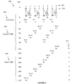
- FIG. 6 is an exemplary demultiplexing algorithm 600 for an eight-sensor array.
- Demultiplexing algorithm 600 includes eight modulations 601 , multiplexed samples 602 for each modulation, and ⁇ - ⁇ code representations 603 for each of a 1 st -order 604 , 2 nd -order 605 , and 3 rd -order 606 .
- the input value of each sensor 607 is the result of performing demultiplexing algorithm 600 .
- Each ⁇ - ⁇ representation in demultiplexing algorithm 600 is calculated by either adding or subtracting adjacent pairs of components of each of the previous order's ⁇ - ⁇ representations.
- the two 1 st -order ⁇ - ⁇ representations 604 ( ⁇ and ⁇ ) are calculated by subtracting and adding pairs of the multiplexed samples.
- the four 2 nd -order ⁇ - ⁇ representations 605 ( ⁇ , ⁇ , ⁇ , and ⁇ ) are then calculated by subtracting or adding adjacent pairs of components of the 1 st -order ⁇ - ⁇ representations ( ⁇ and ⁇ ).
- the eight 3rd-order ⁇ - ⁇ representations 606 are calculated by subtracting or adding adjacent pairs of components of the 2 nd -order ⁇ - ⁇ representations.
- Each of the resulting 3 rd -order ⁇ - ⁇ representations must be divided by 8 (the number of sensors) to give each sensor's input value 607 .
- FIG. 7 illustrates exemplary logic 700 for implementing a multiplexing scheme, in accordance with the present application.
- Logic 700 includes ripple counter 701 and sixteen modulation clock retime flip flops 711 , 712 , 721 , 722 , 731 , 732 , 733 , 734 , 741 , 742 , 743 , 744 , 745 , 747 , 747 , and 748 .
- Both the ripple counter 701 and modulation clock retime flip flops may comprise multiplexing scheme generator 110 , described above with respect to FIG. 1 .
- Modulation clock 711 is hardcoded to a logical high (“1”).
- Modulation clocks 2 (n ⁇ 1) +1 to 2 n are generated using modulation clocks 1 to 2 (n ⁇ 1) gated with the nth bit of the ripple counter in an XNOR configuration.
- each bit in the ripple counter can modulate two outputs, in a manner similar to the sensor modulation schemes presented above with respect to FIG. 4A-4H .
- an n-bit ripple counter is required for multiplexing schemes with 2 n modulation clocks.
- the modulation of each bit in the ripple counter builds on the modulation of the previous bit in the ripple counter, to generate a modulation scheme in a manner similar to that described above with respect to FIGS. 5A-5F .
- the first bit in ripple counter 701 is used to modulate modulation clocks 711 and 712
- the second bit in ripple counter 701 XNORed with the outputs of 711 and 712 generates modulation clocks 721 and 722
- the third bit in ripple counter 701 XNORed with the outputs of 711 , 712 , 721 , and 722 generates modulation clocks 731 , 732 , 733 , and 734 , respectively
- the fourth bit in ripple counter 701 XNORed with the outputs of 711 , 712 , 721 , 722 , 731 , 732 , 733 , and 734 generates modulation clocks 741 , 742 , 743 , 744 , 745 , 747 , 747 , and 748 , respectively.
- an n-bit ripple counter can generate 2 n modulation clocks, i.e., generate the multiplexing scheme that is implemented by
- Logic 700 is offered by way of example and it will be readily appreciated by one of ordinary skill in the art that any number of equivalent arrangements could be used without deviating from the spirit of the invention.
- FIG. 8 illustrates the circuitry of frequency multiplexed sensor array 800 in accordance with an exemplary embodiment of the present application.
- Frequency multiplexed sensor array 800 comprises a multiplexing scheme generator 810 , a modulation system 820 , a sensor array 830 , a readout device 840 , and a demultiplexer 850 .
- Frequency multiplexed sensor array 800 may comprise frequency multiplexed sensor array 100 described above with respect to FIG. 1 .
- Multiplexing scheme generator 810 may comprise ripple counter 701 of logic 700 described above with respect to FIG. 7 .
- Modulation system 820 may comprise modulation system 120 described above with respect to FIG. 1 .
- Sensor array 830 comprises a 32 ⁇ 32 sensor array.
- Readout device 840 comprises several analog to digital converters for providing a digital readout of the multiplexed signal of the sensors in the sensor array 830 .
- a first-order, sigma-delta analog to digital converter is displayed as readout device 840 ; however, any order sigma-delta architecture or any other analog to digital converter architecture could be used.
- a sigma-delta architecture may provide a simple analog front end that can be integrated onto the sensor and provide the number of bits that can be extracted through over sampling.
- the sigma-delta architecture provides the dynamic range necessary to extract a weak signal from the sensors.
- the resolution of the analog to digital converter may vary depending on the application. Accordingly, the 8-bit analog digital converter in readout device 840 is offered by way of example only and some applications may require larger or smaller resolution, including, for example, 20-24 bits.
- Readout device 840 may comprise readout device 130 described above with respect to FIG. 1 .
- Demultiplexer 850 comprises a microcontroller and associated memory.
- the associated memory may comprise First-in First-out (FIFO) memory blocks.
- Demultiplexer 850 may comprise demultiplexer 150 described above with respect to FIG. 1 .
- the FIFOs store data until the microcontroller is ready to process it, thereby allowing the microcontroller and readout device to operate at different rates.
- the microcontroller employs an algorithm to demodulate the sample signals based on the modulation scheme.
- Demultiplexer 850 may comprise demultiplexing algorithm 600 described above with respect to FIG. 6 .
- Frequency multiplexed sensor array 800 is offered by way of example and should not be understood as a limiting embodiment of the present invention. It should be noted that any algorithm could be employed in the microcontroller discussed above. Further, a microcontroller need not be employed and alternative means for demultiplexing the samples are contemplated, such as, for example, a field-programmable gate array or other hardware devices operable to implement logical function.
- FIG. 9 is a block diagram of a process 900 of determining the electrical signal of each of a plurality of electrically connected sensors in a sensor array, according to an exemplary embodiment of the present application. It should be appreciated that process 900 may include any number of additional or alternative tasks. The tasks shown in FIG. 9 need not be performed in the illustrated order, and process 900 may be incorporated into a more comprehensive procedure or process having additional functionality not described in detail herein. Process 900 may be implemented using the embodiments illustrated in FIGS. 1-8 and, for illustrative purposes, the following description of process 900 may refer to elements mentioned above in connection with FIGS. 1-8 .
- process 900 includes multiplexing 901 a plurality of sensors of the sensor array (for example, sensor array 130 described with respect to FIG. 1 ), wherein multiplexing a plurality of sensors comprises selectively reversing the polarity of each sensor.
- Step 901 may also include providing a multiplexing scheme generator for determining which sensors are polarity-reversed for each modulation.
- Step 901 may also include providing a modulation system for implementing a multiplexing scheme.
- process 900 includes measuring 902 a plurality of samples of the plurality of multiplexed sensors (using readout device 140 described with respect to FIG. 1 , for example).
- the number of samples must be at least the number of sensors in the sensor array.
- Process 900 also includes varying 903 the polarity of the plurality of sensors for each of the plurality of samples so that the plurality of samples can be demultiplexed to determine the electrical signal of each sensor.
- varying 903 the polarity of the plurality of sensors is controlled by a multiplexing scheme (not shown) and implemented by a modulation system (not shown).
- process 900 includes demultiplexing 904 the plurality of samples (using demultiplexer 150 described with respect to FIG. 1 , for example).
Landscapes
- Engineering & Computer Science (AREA)
- Multimedia (AREA)
- Signal Processing (AREA)
- Physics & Mathematics (AREA)
- General Physics & Mathematics (AREA)
- Spectroscopy & Molecular Physics (AREA)
- Arrangements For Transmission Of Measured Signals (AREA)
- Solid State Image Pick-Up Elements (AREA)
- Transforming Light Signals Into Electric Signals (AREA)
Priority Applications (6)
| Application Number | Priority Date | Filing Date | Title |
|---|---|---|---|
| US12/826,449 US8320403B2 (en) | 2010-06-29 | 2010-06-29 | Multiplexed sensor array |
| JP2013516923A JP5791714B2 (ja) | 2010-06-29 | 2011-05-19 | 多重化センサアレイ |
| CN2011800326462A CN102971773A (zh) | 2010-06-29 | 2011-05-19 | 复用传感器阵列 |
| PCT/CA2011/000589 WO2012000079A1 (en) | 2010-06-29 | 2011-05-19 | Multiplexed sensor array |
| EP11800003.3A EP2589034B1 (de) | 2010-06-29 | 2011-05-19 | Multiplex-sensorgruppe |
| TW100117963A TW201200848A (en) | 2010-06-29 | 2011-05-23 | Multiplexed sensor array |
Applications Claiming Priority (1)
| Application Number | Priority Date | Filing Date | Title |
|---|---|---|---|
| US12/826,449 US8320403B2 (en) | 2010-06-29 | 2010-06-29 | Multiplexed sensor array |
Publications (2)
| Publication Number | Publication Date |
|---|---|
| US20110317715A1 US20110317715A1 (en) | 2011-12-29 |
| US8320403B2 true US8320403B2 (en) | 2012-11-27 |
Family
ID=45352524
Family Applications (1)
| Application Number | Title | Priority Date | Filing Date |
|---|---|---|---|
| US12/826,449 Active 2031-06-03 US8320403B2 (en) | 2010-06-29 | 2010-06-29 | Multiplexed sensor array |
Country Status (6)
| Country | Link |
|---|---|
| US (1) | US8320403B2 (de) |
| EP (1) | EP2589034B1 (de) |
| JP (1) | JP5791714B2 (de) |
| CN (1) | CN102971773A (de) |
| TW (1) | TW201200848A (de) |
| WO (1) | WO2012000079A1 (de) |
Cited By (1)
| Publication number | Priority date | Publication date | Assignee | Title |
|---|---|---|---|---|
| US10990786B2 (en) | 2018-11-30 | 2021-04-27 | Japan Display Inc. | Detection apparatus |
Families Citing this family (11)
| Publication number | Priority date | Publication date | Assignee | Title |
|---|---|---|---|---|
| EP2828839B1 (de) * | 2012-03-20 | 2017-10-25 | Philips Lighting Holding B.V. | Interferenzerkennung in einem netzwerk von aktiven sensoren |
| US9918029B2 (en) * | 2013-03-14 | 2018-03-13 | Semiconductor Components Industries, Llc | Imaging systems with switchable column power control |
| WO2014174502A2 (en) * | 2013-04-21 | 2014-10-30 | Mizur Technology Ltd. | Tuned sensor arrays and methods of constructing and using same |
| EP2904431B1 (de) * | 2013-12-26 | 2017-07-26 | Halliburton Energy Services, Inc. | Vorrichtung und verfahren zur verringerung von fehlern in messungen |
| JP6278730B2 (ja) * | 2014-02-20 | 2018-02-14 | オリンパス株式会社 | 固体撮像装置および撮像システム |
| EP3359932B1 (de) | 2015-10-05 | 2024-12-25 | Heimann Sensor GmbH | Hochauflösendes thermopile infrarot sensorarray mit monolithisch integrierter signalverarbeitung |
| JP6592402B2 (ja) | 2016-06-03 | 2019-10-16 | 株式会社日立ハイテクノロジーズ | 生体分子計測装置 |
| CN109951411A (zh) * | 2019-04-01 | 2019-06-28 | 南京八云七度生物技术有限公司 | 一种基于频率调制和频分多路复用的传感器阵列数据采集系统 |
| IT201900006735A1 (it) * | 2019-05-10 | 2020-11-10 | Sacertis S R L | Metodo di indagine di una struttura e procedimento per definire una modalità ottimale d’indagine della struttura stessa |
| CN113203348B (zh) * | 2021-04-30 | 2022-07-12 | 中国科学院物理研究所 | 一种纤维型热电模块多区域识别器及其制备方法 |
| FR3154493B1 (fr) * | 2023-10-20 | 2025-10-31 | Commissariat Energie Atomique | Détecteur thermique d’un rayonnement électromagnétique comportant un transducteur thermomètres à diodes |
Citations (15)
| Publication number | Priority date | Publication date | Assignee | Title |
|---|---|---|---|---|
| US5333088A (en) | 1990-12-12 | 1994-07-26 | British Gas Plc | Data transmission system |
| US5717458A (en) | 1994-02-21 | 1998-02-10 | Sony Corporation | Solid-state imager having capacitors connected to vertical signal lines and a charge detection circuit |
| US5847862A (en) | 1995-06-12 | 1998-12-08 | Lucent Technologies Incorporated | Multi-channel optical fiber communication system |
| CA2318305A1 (en) | 1998-01-09 | 1999-07-15 | Eg&G Holdings, Inc. | Method and apparatus for amplifying input signals in one of multiple modes of resolution |
| US6067113A (en) | 1996-09-12 | 2000-05-23 | Vsli Vision Limited | Offset noise cancellation in array image sensors |
| US6078356A (en) | 1992-06-08 | 2000-06-20 | Raytheon Company | Frequency multiplexed data from detector array |
| US6310571B1 (en) * | 2001-03-30 | 2001-10-30 | Pixim, Incorporated | Multiplexed multi-channel bit serial analog-to-digital converter |
| US6714742B1 (en) | 1999-05-20 | 2004-03-30 | University Of Southern California | Polarization-division multiplexing based on power encoding of different polarization channels |
| US20050062460A1 (en) | 2003-09-05 | 2005-03-24 | Blake Jame N. | Time division multiplexed optical measuring system |
| US20050258821A1 (en) | 2004-05-12 | 2005-11-24 | Wang Shan X | Magnetic sensor array having an analog frequency-division multiplexed output |
| US20060034569A1 (en) * | 2004-08-11 | 2006-02-16 | General Electric Company | Novel folded Mach-Zehnder interferometers and optical sensor arrays |
| US20070113681A1 (en) * | 2005-11-22 | 2007-05-24 | Nishimura Ken A | Pressure distribution sensor and sensing method |
| US20070152747A1 (en) | 2004-11-30 | 2007-07-05 | Northrop Grumman Corporation | Multiplexed amplifier |
| US20070194629A1 (en) | 2004-03-09 | 2007-08-23 | Rie Itoh | Frequency sensor and semiconductor device |
| US20110216626A1 (en) * | 2010-03-05 | 2011-09-08 | Itt Manufacturing Enterprises, Inc. | Digital hydrophone |
Family Cites Families (9)
| Publication number | Priority date | Publication date | Assignee | Title |
|---|---|---|---|---|
| KR880009387A (ko) * | 1987-01-30 | 1988-09-15 | 더머 제트.엘 | 진단 모니터링을 위한 스마트센서 시스템 |
| JPH04137200A (ja) * | 1990-09-28 | 1992-05-12 | Okuma Mach Works Ltd | センサー出力信号読取装置 |
| JPH0829899A (ja) * | 1994-07-15 | 1996-02-02 | Fuji Photo Film Co Ltd | 放射線画像情報読取システム |
| JP3675984B2 (ja) * | 1996-09-12 | 2005-07-27 | 株式会社ルネサステクノロジ | 受光素子回路及び受光素子回路アレイ |
| US5964708A (en) * | 1997-10-06 | 1999-10-12 | The Regents Of The University Of Michigan | Beamformed ultrasonic imager with delta-sigma feedback control |
| TW522723B (en) * | 2000-08-15 | 2003-03-01 | Pixim Inc | Circuit and method for pixel rearrangement in a digital pixel sensor readout |
| JP4554112B2 (ja) * | 2001-06-21 | 2010-09-29 | 三井造船株式会社 | 二次元微弱放射検出装置 |
| JP2006098223A (ja) * | 2004-09-29 | 2006-04-13 | Sanyo Electric Co Ltd | ノイズ除去回路及びそれを備えた温度測定処理装置 |
| US7488928B2 (en) * | 2007-04-20 | 2009-02-10 | Alexander Krymski | Image sensor circuits and methods with multiple readout lines per column of pixel circuits |
-
2010
- 2010-06-29 US US12/826,449 patent/US8320403B2/en active Active
-
2011
- 2011-05-19 JP JP2013516923A patent/JP5791714B2/ja not_active Expired - Fee Related
- 2011-05-19 WO PCT/CA2011/000589 patent/WO2012000079A1/en not_active Ceased
- 2011-05-19 EP EP11800003.3A patent/EP2589034B1/de not_active Not-in-force
- 2011-05-19 CN CN2011800326462A patent/CN102971773A/zh active Pending
- 2011-05-23 TW TW100117963A patent/TW201200848A/zh unknown
Patent Citations (15)
| Publication number | Priority date | Publication date | Assignee | Title |
|---|---|---|---|---|
| US5333088A (en) | 1990-12-12 | 1994-07-26 | British Gas Plc | Data transmission system |
| US6078356A (en) | 1992-06-08 | 2000-06-20 | Raytheon Company | Frequency multiplexed data from detector array |
| US5717458A (en) | 1994-02-21 | 1998-02-10 | Sony Corporation | Solid-state imager having capacitors connected to vertical signal lines and a charge detection circuit |
| US5847862A (en) | 1995-06-12 | 1998-12-08 | Lucent Technologies Incorporated | Multi-channel optical fiber communication system |
| US6067113A (en) | 1996-09-12 | 2000-05-23 | Vsli Vision Limited | Offset noise cancellation in array image sensors |
| CA2318305A1 (en) | 1998-01-09 | 1999-07-15 | Eg&G Holdings, Inc. | Method and apparatus for amplifying input signals in one of multiple modes of resolution |
| US6714742B1 (en) | 1999-05-20 | 2004-03-30 | University Of Southern California | Polarization-division multiplexing based on power encoding of different polarization channels |
| US6310571B1 (en) * | 2001-03-30 | 2001-10-30 | Pixim, Incorporated | Multiplexed multi-channel bit serial analog-to-digital converter |
| US20050062460A1 (en) | 2003-09-05 | 2005-03-24 | Blake Jame N. | Time division multiplexed optical measuring system |
| US20070194629A1 (en) | 2004-03-09 | 2007-08-23 | Rie Itoh | Frequency sensor and semiconductor device |
| US20050258821A1 (en) | 2004-05-12 | 2005-11-24 | Wang Shan X | Magnetic sensor array having an analog frequency-division multiplexed output |
| US20060034569A1 (en) * | 2004-08-11 | 2006-02-16 | General Electric Company | Novel folded Mach-Zehnder interferometers and optical sensor arrays |
| US20070152747A1 (en) | 2004-11-30 | 2007-07-05 | Northrop Grumman Corporation | Multiplexed amplifier |
| US20070113681A1 (en) * | 2005-11-22 | 2007-05-24 | Nishimura Ken A | Pressure distribution sensor and sensing method |
| US20110216626A1 (en) * | 2010-03-05 | 2011-09-08 | Itt Manufacturing Enterprises, Inc. | Digital hydrophone |
Non-Patent Citations (4)
| Title |
|---|
| Hanson, Uncooled Thermal Imaging Detectors and Systems, SPIE (2010) pp. 1-187. |
| International Search Report and Written Opinion received in PCT Patent Application No. PCT/CA2011/000589, mailed on Sep. 15, 2011, 7 pages. |
| Kolling et al., (1989) Two-lead multiplex system for sensor array applicaitons, Sensors and Actuators, 17 (3-4). pp. 623-628 ISSN 0250-6874. * |
| Kruse, Uncooled Thermal Imaging: Arrays, Systems, and Applications, SPIE Press (2002) pp. 1-89. |
Cited By (2)
| Publication number | Priority date | Publication date | Assignee | Title |
|---|---|---|---|---|
| US10990786B2 (en) | 2018-11-30 | 2021-04-27 | Japan Display Inc. | Detection apparatus |
| US11263425B2 (en) | 2018-11-30 | 2022-03-01 | Japan Display Inc. | Detection apparatus |
Also Published As
| Publication number | Publication date |
|---|---|
| EP2589034A4 (de) | 2015-05-27 |
| EP2589034B1 (de) | 2017-04-05 |
| US20110317715A1 (en) | 2011-12-29 |
| WO2012000079A1 (en) | 2012-01-05 |
| JP5791714B2 (ja) | 2015-10-07 |
| CN102971773A (zh) | 2013-03-13 |
| JP2013535162A (ja) | 2013-09-09 |
| EP2589034A1 (de) | 2013-05-08 |
| TW201200848A (en) | 2012-01-01 |
Similar Documents
| Publication | Publication Date | Title |
|---|---|---|
| US8320403B2 (en) | Multiplexed sensor array | |
| US6809666B1 (en) | Circuit and method for gray code to binary conversion | |
| KR20210127937A (ko) | 시간 인터리브드 아날로그-디지털 컨버터에서 절단 스위치 불일치를 교정하는 회로 | |
| CN105093258A (zh) | 光子测量前端电路 | |
| KR101743800B1 (ko) | A/d 변환기, 이미지 센서 디바이스 및 아날로그 신호로부터 디지털 신호를 생성하는 방법 | |
| Fick et al. | Mixed-signal stochastic computation demonstrated in an image sensor with integrated 2D edge detection and noise filtering | |
| EP2834969B1 (de) | Pixelverarbeitungsschaltung | |
| US7847719B2 (en) | Signal processors, signal processing methods, and digital filter configuration methods | |
| CN203590324U (zh) | 列并行模数转换器及cmos图像传感器 | |
| EP3764251B1 (de) | Diskrete berechnung einer transformation der zeitdomäne | |
| CN110730062B (zh) | 一种基于模板攻击的混沌分组加密分析方法 | |
| Reis et al. | Using synchronism pulse to improve a2i implementations | |
| US9847789B1 (en) | High precision sampled analog circuits | |
| Khani et al. | Digital realization of twisted tent map and ship map with LFSR as a pseudo-chaos generator | |
| Rosato et al. | Perfect reconstruction filters for 4-channels time-interleaved ADC affected by mismatches | |
| Akgun et al. | An energy-efficient multi-sensor compressed sensing system employing time-mode signal processing techniques | |
| Ibrahim et al. | FPGA Hardware Accelerator for Image Encryption/Decryption System Using Henon Chaos Addressing and Embedded Block RAM | |
| SU1749842A1 (ru) | Цифровой измеритель электрической энергии | |
| KR100247957B1 (ko) | 직병렬 곱셈기를 이용한 iir 필터 | |
| RU2187886C1 (ru) | Устройство для преобразования чисел из кода системы остаточных классов в полиадический код | |
| Craigen et al. | Constructions for Circulant and Group‐Developed Generalized Weighing Matrices | |
| RU104336U1 (ru) | Генератор псевдослучайных последовательностей | |
| ASCI et al. | A MIXED CODING/DECODING ALGORITHM BASED ON COMPLEX RECURRENCE RELATIONS | |
| RU2133499C1 (ru) | Устройство определения математического ожидания нестационарного случайного процесса семиотического типа | |
| Edirisuriya | Digital Hardware Architectures for Exact and Approximate DCT Computation Using Number Theoretic Techniques |
Legal Events
| Date | Code | Title | Description |
|---|---|---|---|
| AS | Assignment |
Owner name: PERKINELMER CANADA, INC., CANADA Free format text: ASSIGNMENT OF ASSIGNORS INTEREST;ASSIGNOR:HOOD, SHELDON JAMES;REEL/FRAME:024883/0063 Effective date: 20100820 |
|
| AS | Assignment |
Owner name: EXCELITAS CANADA INC., CANADA Free format text: MERGER;ASSIGNORS:PERKINELMER CANADA INC.;EXCELITAS CANADA INC.;REEL/FRAME:027052/0975 Effective date: 20101129 |
|
| STCF | Information on status: patent grant |
Free format text: PATENTED CASE |
|
| AS | Assignment |
Owner name: EXCELITAS TECHNOLOGIES SINGAPORE PTE. LTD., SINGAP Free format text: ASSIGNMENT OF ASSIGNORS INTEREST;ASSIGNOR:EXCELITAS CANADA, INC.;REEL/FRAME:030076/0456 Effective date: 20130321 |
|
| FPAY | Fee payment |
Year of fee payment: 4 |
|
| MAFP | Maintenance fee payment |
Free format text: PAYMENT OF MAINTENANCE FEE, 8TH YEAR, LARGE ENTITY (ORIGINAL EVENT CODE: M1552); ENTITY STATUS OF PATENT OWNER: LARGE ENTITY Year of fee payment: 8 |
|
| MAFP | Maintenance fee payment |
Free format text: PAYMENT OF MAINTENANCE FEE, 12TH YEAR, LARGE ENTITY (ORIGINAL EVENT CODE: M1553); ENTITY STATUS OF PATENT OWNER: LARGE ENTITY Year of fee payment: 12 |