US8569671B2 - Pixel array capable of performing pipelined global shutter operation including a first and second buffer amplifier - Google Patents
Pixel array capable of performing pipelined global shutter operation including a first and second buffer amplifier Download PDFInfo
- Publication number
- US8569671B2 US8569671B2 US12/408,975 US40897509A US8569671B2 US 8569671 B2 US8569671 B2 US 8569671B2 US 40897509 A US40897509 A US 40897509A US 8569671 B2 US8569671 B2 US 8569671B2
- Authority
- US
- United States
- Prior art keywords
- sample
- pixel
- sense node
- reset
- sample stage
- Prior art date
- Legal status (The legal status is an assumption and is not a legal conclusion. Google has not performed a legal analysis and makes no representation as to the accuracy of the status listed.)
- Active, expires
Links
Images


Classifications
-
- H—ELECTRICITY
- H10—SEMICONDUCTOR DEVICES; ELECTRIC SOLID-STATE DEVICES NOT OTHERWISE PROVIDED FOR
- H10F—INORGANIC SEMICONDUCTOR DEVICES SENSITIVE TO INFRARED RADIATION, LIGHT, ELECTROMAGNETIC RADIATION OF SHORTER WAVELENGTH OR CORPUSCULAR RADIATION
- H10F39/00—Integrated devices, or assemblies of multiple devices, comprising at least one element covered by group H10F30/00, e.g. radiation detectors comprising photodiode arrays
- H10F39/80—Constructional details of image sensors
- H10F39/803—Pixels having integrated switching, control, storage or amplification elements
- H10F39/8037—Pixels having integrated switching, control, storage or amplification elements the integrated elements comprising a transistor
-
- H—ELECTRICITY
- H04—ELECTRIC COMMUNICATION TECHNIQUE
- H04N—PICTORIAL COMMUNICATION, e.g. TELEVISION
- H04N25/00—Circuitry of solid-state image sensors [SSIS]; Control thereof
- H04N25/50—Control of the SSIS exposure
- H04N25/53—Control of the integration time
- H04N25/532—Control of the integration time by controlling global shutters in CMOS SSIS
-
- H—ELECTRICITY
- H04—ELECTRIC COMMUNICATION TECHNIQUE
- H04N—PICTORIAL COMMUNICATION, e.g. TELEVISION
- H04N25/00—Circuitry of solid-state image sensors [SSIS]; Control thereof
- H04N25/50—Control of the SSIS exposure
- H04N25/57—Control of the dynamic range
- H04N25/59—Control of the dynamic range by controlling the amount of charge storable in the pixel, e.g. modification of the charge conversion ratio of the floating node capacitance
-
- H—ELECTRICITY
- H04—ELECTRIC COMMUNICATION TECHNIQUE
- H04N—PICTORIAL COMMUNICATION, e.g. TELEVISION
- H04N25/00—Circuitry of solid-state image sensors [SSIS]; Control thereof
- H04N25/60—Noise processing, e.g. detecting, correcting, reducing or removing noise
- H04N25/616—Noise processing, e.g. detecting, correcting, reducing or removing noise involving a correlated sampling function, e.g. correlated double sampling [CDS] or triple sampling
-
- H—ELECTRICITY
- H04—ELECTRIC COMMUNICATION TECHNIQUE
- H04N—PICTORIAL COMMUNICATION, e.g. TELEVISION
- H04N25/00—Circuitry of solid-state image sensors [SSIS]; Control thereof
- H04N25/60—Noise processing, e.g. detecting, correcting, reducing or removing noise
- H04N25/65—Noise processing, e.g. detecting, correcting, reducing or removing noise applied to reset noise, e.g. KTC noise related to CMOS structures by techniques other than CDS
-
- H—ELECTRICITY
- H04—ELECTRIC COMMUNICATION TECHNIQUE
- H04N—PICTORIAL COMMUNICATION, e.g. TELEVISION
- H04N25/00—Circuitry of solid-state image sensors [SSIS]; Control thereof
- H04N25/70—SSIS architectures; Circuits associated therewith
- H04N25/703—SSIS architectures incorporating pixels for producing signals other than image signals
- H04N25/707—Pixels for event detection
-
- H—ELECTRICITY
- H04—ELECTRIC COMMUNICATION TECHNIQUE
- H04N—PICTORIAL COMMUNICATION, e.g. TELEVISION
- H04N25/00—Circuitry of solid-state image sensors [SSIS]; Control thereof
- H04N25/70—SSIS architectures; Circuits associated therewith
- H04N25/76—Addressed sensors, e.g. MOS or CMOS sensors
- H04N25/77—Pixel circuitry, e.g. memories, A/D converters, pixel amplifiers, shared circuits or shared components
- H04N25/771—Pixel circuitry, e.g. memories, A/D converters, pixel amplifiers, shared circuits or shared components comprising storage means other than floating diffusion
-
- H—ELECTRICITY
- H04—ELECTRIC COMMUNICATION TECHNIQUE
- H04N—PICTORIAL COMMUNICATION, e.g. TELEVISION
- H04N25/00—Circuitry of solid-state image sensors [SSIS]; Control thereof
- H04N25/70—SSIS architectures; Circuits associated therewith
- H04N25/76—Addressed sensors, e.g. MOS or CMOS sensors
- H04N25/78—Readout circuits for addressed sensors, e.g. output amplifiers or A/D converters
Definitions
- a photo-sensitive element for generating charges in response to incident radiation
- the pixel, or pixel array is fabricated in CMOS technology.
- Another aspect of the invention provides methods of operating a pixel, or a pixel array as described herein, or as defined in any of the claims.
- some steps can be performed in a different order to the order recited in the claims, without deviating from the scope of the invention.
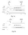
- FIGS. 13 a and 13 b show timing diagrams for operation of the pixels of FIGS. 11 and 12 respectively;
- the second switch and capacitor in the amplifier are used as a track and hold. This stage will track the signal (switch closed) when the subtracted signal is available at the output of the first buffer (this is when the second sample is applied), and will be in hold (switch open) when the first sample is applied (the differential signal of the previous sample is then still available at the output of the output amplifier).
- a column processing unit associated with each column of the pixel array can perform an analog-to-digital conversion of the difference between the reset level and the sample signal.
- the image is read out by reading the values stored in the pixel capacitors C reset and C signal . During readout, the difference between the two signals is calculated. This cancels any kTC noise on the floating diffusion, and it is thus a true correlated double sampling readout. During this readout, the photodiode can be exposed to radiation for the next frame.
Landscapes
- Engineering & Computer Science (AREA)
- Multimedia (AREA)
- Signal Processing (AREA)
- Transforming Light Signals Into Electric Signals (AREA)
- Solid State Image Pick-Up Elements (AREA)
- Apparatus For Radiation Diagnosis (AREA)
Priority Applications (2)
| Application Number | Priority Date | Filing Date | Title |
|---|---|---|---|
| US13/344,095 US8754357B2 (en) | 2008-04-07 | 2012-01-05 | Pixel having two cascade-connected sample stages, pixel array, and method of operating same |
| US14/268,106 US20140239161A1 (en) | 2008-04-07 | 2014-05-02 | Pixel Array With Global Shutter |
Applications Claiming Priority (5)
| Application Number | Priority Date | Filing Date | Title |
|---|---|---|---|
| GB0806274A GB0806274D0 (en) | 2008-04-07 | 2008-04-07 | Pixel array with global shutter |
| GB0806274.7 | 2008-04-07 | ||
| EP08166987 | 2008-10-17 | ||
| EP08166987.1 | 2008-10-17 | ||
| EP08166987 | 2008-10-17 |
Related Child Applications (1)
| Application Number | Title | Priority Date | Filing Date |
|---|---|---|---|
| US13/344,095 Division US8754357B2 (en) | 2008-04-07 | 2012-01-05 | Pixel having two cascade-connected sample stages, pixel array, and method of operating same |
Publications (2)
| Publication Number | Publication Date |
|---|---|
| US20090256060A1 US20090256060A1 (en) | 2009-10-15 |
| US8569671B2 true US8569671B2 (en) | 2013-10-29 |
Family
ID=40810287
Family Applications (3)
| Application Number | Title | Priority Date | Filing Date |
|---|---|---|---|
| US12/408,975 Active 2030-02-04 US8569671B2 (en) | 2008-04-07 | 2009-03-23 | Pixel array capable of performing pipelined global shutter operation including a first and second buffer amplifier |
| US13/344,095 Active US8754357B2 (en) | 2008-04-07 | 2012-01-05 | Pixel having two cascade-connected sample stages, pixel array, and method of operating same |
| US14/268,106 Abandoned US20140239161A1 (en) | 2008-04-07 | 2014-05-02 | Pixel Array With Global Shutter |
Family Applications After (2)
| Application Number | Title | Priority Date | Filing Date |
|---|---|---|---|
| US13/344,095 Active US8754357B2 (en) | 2008-04-07 | 2012-01-05 | Pixel having two cascade-connected sample stages, pixel array, and method of operating same |
| US14/268,106 Abandoned US20140239161A1 (en) | 2008-04-07 | 2014-05-02 | Pixel Array With Global Shutter |
Country Status (2)
| Country | Link |
|---|---|
| US (3) | US8569671B2 (de) |
| EP (3) | EP2587794B1 (de) |
Cited By (20)
| Publication number | Priority date | Publication date | Assignee | Title |
|---|---|---|---|---|
| US20110267510A1 (en) * | 2010-05-03 | 2011-11-03 | Malone Michael R | Devices and methods for high-resolution image and video capture |
| US20130020463A1 (en) * | 2011-07-21 | 2013-01-24 | Tae-Yon Lee | Image-sensing devices and methods of operating the same |
| US20140239161A1 (en) * | 2008-04-07 | 2014-08-28 | Cmosis Nv | Pixel Array With Global Shutter |
| US20140312208A1 (en) * | 2008-11-20 | 2014-10-23 | Canon Kabushiki Kaisha | Drive circuit for semiconductor image sensor array |
| US20150312502A1 (en) * | 2014-03-25 | 2015-10-29 | Imec Vzw | Imaging sensor |
| DE102015116026A1 (de) | 2015-09-22 | 2017-03-23 | JENETRIC GmbH | Vorrichtung und Verfahren zur direkten optischen Bildaufnahme von Dokumenten und / oder lebenden Hautbereichen ohne abbildende optische Elemente |
| US10225499B2 (en) | 2016-04-11 | 2019-03-05 | Semiconductor Components Industries, Llc | Backside illuminated global shutter pixel with active reset |
| WO2019115459A1 (en) | 2017-12-15 | 2019-06-20 | Ams Ag | Pixel structure, image sensor device and system with pixel structure, and method of operating the pixel structure |
| US20200260021A1 (en) * | 2018-12-13 | 2020-08-13 | Facebook Technologies, Llc | Differentiated imaging using camera assembly with augmented pixels |
| US10791282B2 (en) | 2018-12-13 | 2020-09-29 | Fenwick & West LLP | High dynamic range camera assembly with augmented pixels |
| US10855896B1 (en) | 2018-12-13 | 2020-12-01 | Facebook Technologies, Llc | Depth determination using time-of-flight and camera assembly with augmented pixels |
| US10902623B1 (en) | 2019-11-19 | 2021-01-26 | Facebook Technologies, Llc | Three-dimensional imaging with spatial and temporal coding for depth camera assembly |
| US20210235027A1 (en) * | 2018-08-03 | 2021-07-29 | Ams Sensors Belgium Bvba | Pixel cell and method for operating a pixel cell |
| US11194160B1 (en) | 2020-01-21 | 2021-12-07 | Facebook Technologies, Llc | High frame rate reconstruction with N-tap camera sensor |
| US20220060645A1 (en) * | 2016-03-31 | 2022-02-24 | Sony Group Corporation | Imaging apparatus, driving method, and electronic device |
| US11317050B2 (en) | 2005-03-11 | 2022-04-26 | Hand Held Products, Inc. | Image reader comprising CMOS based image sensor array |
| US20230007204A1 (en) * | 2020-03-17 | 2023-01-05 | Shenzhen Rgbic Microelectronics Technology Co., Ltd | Pixel circuit, image sensor, and image pickup device and method for using the same |
| US11604933B2 (en) | 2005-06-03 | 2023-03-14 | Hand Held Products, Inc. | Apparatus having hybrid monochrome and color image sensor array |
| US11653110B2 (en) | 2020-09-18 | 2023-05-16 | Samsung Electronics Co., Ltd. | Image sensor |
| US12495219B2 (en) | 2020-09-18 | 2025-12-09 | Samsung Electronics Co., Ltd. | Image sensor |
Families Citing this family (77)
| Publication number | Priority date | Publication date | Assignee | Title |
|---|---|---|---|---|
| FR2937131B1 (fr) * | 2008-10-15 | 2011-01-28 | Soc Fr Detecteurs Infrarouges Sofradir | Procede et dispositif de lecture de charges electriques produites par un photodetecteur, et detecteur comportant de tels dispositifs |
| JP5001970B2 (ja) * | 2009-03-30 | 2012-08-15 | 浜松ホトニクス株式会社 | 固体撮像装置 |
| US8405017B2 (en) * | 2009-12-24 | 2013-03-26 | Imagerlabs Inc. | Adjustable CMOS sensor array |
| US8324550B2 (en) * | 2010-06-22 | 2012-12-04 | Aptina Imaging Corporation | High dynamic range imaging systems |
| KR101171778B1 (ko) * | 2010-08-16 | 2012-08-06 | 주식회사 동부하이텍 | 수동형 이미지 센서 및 그 동작 방법 |
| GB2487943A (en) * | 2011-02-09 | 2012-08-15 | St Microelectronics Res & Dev | A CMOS pixel sensor with local analogue storage in each pixel circuit for capturing frames in quick succession |
| US8987646B2 (en) * | 2011-06-10 | 2015-03-24 | Semiconductor Components Industries, Llc | Pixel and method |
| GB2492387B (en) | 2011-06-30 | 2017-07-19 | Cmosis Nv | Pixel array with individual exposure control for a pixel or pixel region |
| JP5755111B2 (ja) * | 2011-11-14 | 2015-07-29 | キヤノン株式会社 | 撮像装置の駆動方法 |
| JP6327779B2 (ja) * | 2012-02-29 | 2018-05-23 | キヤノン株式会社 | 光電変換装置、焦点検出装置および撮像システム |
| US8953075B2 (en) * | 2012-03-30 | 2015-02-10 | Pixim, Inc. | CMOS image sensors implementing full frame digital correlated double sampling with global shutter |
| US9601538B2 (en) * | 2012-05-03 | 2017-03-21 | Semiconductor Components Industries, Llc | Image sensors with photoelectric films |
| US8779346B2 (en) * | 2012-05-14 | 2014-07-15 | BAE Systems Imaging Solutions Inc. | Digital pixel sensor with reduced noise |
| US8975570B2 (en) | 2012-08-23 | 2015-03-10 | Teledyne Dalsa Inc. | CMOS time delay and integration image sensor |
| US9148601B2 (en) | 2012-09-26 | 2015-09-29 | Teledyne Dalsa, Inc. | CMOS TDI image sensor with rolling shutter pixels |
| GB201302664D0 (en) | 2013-02-15 | 2013-04-03 | Cmosis Nv | A pixel structure |
| US20140270572A1 (en) * | 2013-03-13 | 2014-09-18 | Himax Imaging, Inc. | Signal processing apparatus and method for detecting/correcting eclipse phenomenon, and related correlated double sampling apparatus |
| CN103259985B (zh) | 2013-05-17 | 2016-08-17 | 昆山锐芯微电子有限公司 | Cmos图像传感器、像素单元及其控制方法 |
| KR20150000250A (ko) | 2013-06-24 | 2015-01-02 | 삼성전자주식회사 | 단위 픽셀 및 그것을 포함하는 이미지 센서 |
| US9412782B2 (en) * | 2013-07-08 | 2016-08-09 | BAE Systems Imaging Solutions Inc. | Imaging array with improved dynamic range utilizing parasitic photodiodes within floating diffusion nodes of pixels |
| US10128296B2 (en) | 2013-07-08 | 2018-11-13 | BAE Systems Imaging Solutions Inc. | Imaging array with improved dynamic range utilizing parasitic photodiodes |
| GB2517444A (en) * | 2013-08-20 | 2015-02-25 | Cmosis Bvba | Pixel for global shutter operation |
| CN104427270A (zh) * | 2013-08-28 | 2015-03-18 | 北京计算机技术及应用研究所 | 超高清cmos图像传感器像素电路及其控制方法 |
| FR3010229B1 (fr) | 2013-08-30 | 2016-12-23 | Pyxalis | Capteur d'image avec bruit ktc reduit |
| US9165613B2 (en) * | 2013-09-03 | 2015-10-20 | Taiwan Semiconductor Manufacturing Company, Ltd. | Sample-and-hold current sense amplifier and related method |
| JP6087780B2 (ja) * | 2013-10-10 | 2017-03-01 | ソニーセミコンダクタソリューションズ株式会社 | 撮像素子、放射線検出装置および撮像素子の制御方法 |
| GB201318404D0 (en) | 2013-10-17 | 2013-12-04 | Cmosis Nv | An image sensor |
| KR102135677B1 (ko) | 2013-11-28 | 2020-07-20 | 삼성전자주식회사 | 이미지 센서 및 이미지 센서를 구동하는 방법 |
| US9264639B2 (en) | 2014-02-07 | 2016-02-16 | Rambus Inc. | Feedthrough-compensated image sensor |
| US9479717B2 (en) * | 2014-02-18 | 2016-10-25 | Semiconductor Components Industries, Llc | Image sensor array with external charge detection circuitry |
| DE102015003134B4 (de) | 2014-04-01 | 2017-04-06 | Viimagic Gesellschaft mit beschränkter Haftung | Global-Shutter Pixel und Korrekturverfahren |
| KR102191245B1 (ko) * | 2014-06-20 | 2020-12-15 | 삼성전자주식회사 | 이미지 센서 구동 방법, 이를 채용한 이미지 센서 및 이를 포함하는 휴대용 전자 기기 |
| DE102014013099B4 (de) | 2014-09-03 | 2019-11-14 | Basler Aktiengesellschaft | Verfahren und Vorrichtung zur vereinfachten Erfassung eines Tiefenbildes |
| JP5974202B1 (ja) * | 2014-11-25 | 2016-08-23 | オリンパス株式会社 | 撮像素子、撮像装置、内視鏡および内視鏡システム |
| KR102301620B1 (ko) | 2015-02-02 | 2021-09-14 | 삼성전자주식회사 | 빛 샘 보정을 위한 촬영 장치 및 방법 |
| US9749565B2 (en) | 2015-05-18 | 2017-08-29 | Analog Devices, Inc. | Interline charge-coupled devices |
| EP3101812B1 (de) | 2015-06-05 | 2022-10-26 | Cmosis Bvba | Pixelinterner differenz-transkonduktanzverstärker für adc und bildsensorarchitektur |
| US9843757B2 (en) * | 2015-06-24 | 2017-12-12 | Stmicroelectronics (Research & Development) Limited | Optical electronic device including enhanced global shutter pixel array and related methods |
| JP6740230B2 (ja) * | 2015-07-31 | 2020-08-12 | ソニーセミコンダクタソリューションズ株式会社 | 固体撮像装置および電子機器 |
| JP6799538B2 (ja) * | 2015-08-04 | 2020-12-16 | ヌヴォトンテクノロジージャパン株式会社 | 固体撮像装置の駆動方法 |
| US9521351B1 (en) * | 2015-09-21 | 2016-12-13 | Rambus Inc. | Fractional-readout oversampled image sensor |
| US9736413B1 (en) | 2016-02-03 | 2017-08-15 | Sony Corporation | Image sensor and electronic device with active reset circuit, and method of operating the same |
| US10145734B2 (en) * | 2016-08-22 | 2018-12-04 | Semiconductor Components Industries, Llc | Methods and apparatus for a light sensor |
| US9961279B1 (en) * | 2016-12-20 | 2018-05-01 | Omnivision Technologies, Inc. | Blooming free high dynamic range image sensor read out architecture using in-frame multi-bit exposure control |
| US9955091B1 (en) | 2016-12-20 | 2018-04-24 | Omnivision Technologies, Inc. | High dynamic range image sensor read out architecture using in-frame multi-bit exposure control |
| US9888185B1 (en) * | 2016-12-20 | 2018-02-06 | Omnivision Technologies, Inc. | Row decoder for high dynamic range image sensor using in-frame multi-bit exposure control |
| US10440298B2 (en) * | 2016-12-23 | 2019-10-08 | Bae Systems Information And Electronic Systems Integration Inc. | Extended dynamic range cis pixel achieving ultra-low noise |
| CN110291782B (zh) * | 2017-03-13 | 2020-09-29 | 华为技术有限公司 | Cmos图像传感器 |
| EP3724928B1 (de) | 2017-12-12 | 2023-03-15 | Emberion Oy | Fotoempfindlicher feldeffekt-transistor |
| US10560646B2 (en) | 2018-04-19 | 2020-02-11 | Teledyne Scientific & Imaging, Llc | Global-shutter vertically integrated pixel with high dynamic range |
| TW202005357A (zh) | 2018-05-25 | 2020-01-16 | 原相科技股份有限公司 | 改善像素感測效率的電路 |
| GB2574619B (en) * | 2018-06-12 | 2022-10-12 | Res & Innovation Uk | Image sensor |
| FR3094598A1 (fr) * | 2019-03-29 | 2020-10-02 | Stmicroelectronics (Grenoble 2) Sas | Pixel et son procédé de commande |
| FR3096855B1 (fr) | 2019-06-03 | 2022-08-05 | St Microelectronics Grenoble 2 | Capteur d'image et son procédé de commande |
| FR3096856B1 (fr) | 2019-06-03 | 2021-06-25 | St Microelectronics Grenoble 2 | Capteur d'image et son procédé de commande |
| US10990782B2 (en) * | 2019-09-09 | 2021-04-27 | Novatek Microelectronics Corp. | Operating method of an optical fingerprint capture apparatus and operating method of an optical fingerprint recognition system |
| KR102895535B1 (ko) * | 2019-11-27 | 2025-12-05 | 삼성전자주식회사 | 이미지 센서, 그것을 포함하는 이미지 장치, 및 그것의 동작 방법 |
| FR3103964B1 (fr) | 2019-11-29 | 2021-11-26 | Pyxalis | Pixel à dynamique ajustable pour la réduction de bruit |
| JP7520498B2 (ja) * | 2019-12-02 | 2024-07-23 | ソニーセミコンダクタソリューションズ株式会社 | 固体撮像装置及び電子機器 |
| CN111416953B (zh) * | 2020-02-25 | 2022-12-09 | 深圳市南北微电子技术有限公司 | 全局快门图像传感器像素结构及其信号采样读取方法 |
| CN111447385B (zh) * | 2020-03-17 | 2022-04-19 | 深圳市南北微电子技术有限公司 | 全局快门图像传感器像素结构及其信号采样读取方法 |
| CN111447384B (zh) * | 2020-03-17 | 2022-09-02 | 深圳市南北微电子技术有限公司 | 高动态范围全局快门像素结构及其信号采样读取方法 |
| CN111405211B (zh) * | 2020-03-27 | 2022-09-23 | 上海集成电路研发中心有限公司 | 一种图像传感器像素结构及其控制方法 |
| EP3930309A1 (de) * | 2020-06-26 | 2021-12-29 | ams Sensors Belgium BVBA | Pixel und verfahren zum betrieb eines pixels |
| CN112071254B (zh) * | 2020-09-18 | 2023-12-26 | 京东方科技集团股份有限公司 | 一种时序控制的方法、平板探测器及影像设备 |
| US11153524B1 (en) * | 2020-09-22 | 2021-10-19 | Pixart Imaging Incorporation | High precision pixel circuit and method thereof |
| US11588482B1 (en) * | 2020-11-19 | 2023-02-21 | Hrl Laboratories, Llc | Multiplexing sample-and-hold circuit |
| CN112468744B (zh) * | 2020-11-27 | 2023-05-19 | 京东方科技集团股份有限公司 | 像素电路、光电检测基板、光电检测装置及驱动方法 |
| CN112887571B (zh) * | 2021-01-27 | 2022-06-10 | 维沃移动通信有限公司 | 图像传感器、摄像模组和电子设备 |
| WO2023018841A1 (en) | 2021-08-10 | 2023-02-16 | ams Sensors USA Inc. | Self calibrating barrier modulation pixel |
| JP2024529195A (ja) | 2021-08-10 | 2024-08-02 | エーエムエス・センサーズ・ユーエスエー・インコーポレイテッド | 画素配置および画素配置を動作させるための方法 |
| CN118661424A (zh) | 2022-02-09 | 2024-09-17 | 艾迈斯传感器比利时有限责任公司 | 图像传感器、光电装置和用于操作成像装置的方法 |
| CN118648298A (zh) * | 2022-02-09 | 2024-09-13 | 艾迈斯传感器比利时有限责任公司 | 成像器件、光电器件和用于操作成像器件的方法 |
| KR20230160001A (ko) | 2022-05-16 | 2023-11-23 | 삼성전자주식회사 | 이미지 센서 |
| CN115278100B (zh) * | 2022-07-19 | 2023-10-17 | 杭州海康微影传感科技有限公司 | 一种像素单元电路、信号采集装置和信号采集方法 |
| KR20240116282A (ko) | 2023-01-20 | 2024-07-29 | 삼성전자주식회사 | 이미지 센서 및 상기 이미지 센서의 동작 방법 |
| DE112024000389T5 (de) * | 2023-01-23 | 2025-10-16 | ams Sensors USA Inc. | Pixelanordnung mit zwei transfertransistoren und verfahren zum betreiben einer pixelanordnung |
Citations (13)
| Publication number | Priority date | Publication date | Assignee | Title |
|---|---|---|---|---|
| US4914518A (en) * | 1987-01-19 | 1990-04-03 | Canon Kabushiki Kaisha | Electronic still camera with a solid state image pickup whose output part is kept from being driven during a major part of the image pickup period |
| US5268576A (en) * | 1991-04-04 | 1993-12-07 | Texas Instruments Incorporated | Infrared focal plane array processor with integration and low pass filter per pixel |
| US5461491A (en) * | 1993-12-29 | 1995-10-24 | Hewlett-Packard Company | Procedure for reducing processing time for image elements by combining charge of adjacent pixels into a new composite pixel |
| US6040568A (en) * | 1998-05-06 | 2000-03-21 | Raytheon Company | Multipurpose readout integrated circuit with in cell adaptive non-uniformity correction and enhanced dynamic range |
| US6317154B2 (en) * | 1998-02-27 | 2001-11-13 | Intel Corporation | Method to reduce reset noise in photodiode based CMOS image sensors |
| US20020134913A1 (en) * | 2001-03-22 | 2002-09-26 | Xerox Corporation | Photosensitive apparatus in which an initial charge on a photodiode is sampled and then retransferred to the photodiode |
| US6847070B2 (en) | 2000-08-09 | 2005-01-25 | Dalsa, Inc. | Five transistor CMOS pixel |
| US6847400B2 (en) * | 2001-03-22 | 2005-01-25 | Xerox Corporation | Photosensitive apparatus wherein an initial charge on a photodiode is sampled and substracted during readout |
| US20060192864A1 (en) * | 2005-02-28 | 2006-08-31 | Rick Mauritzson | Imager row-wise noise correction |
| JP2006311008A (ja) | 2005-04-27 | 2006-11-09 | Sony Corp | 撮像装置 |
| US20070096233A1 (en) * | 2005-10-13 | 2007-05-03 | In Gyun Jeon | Cmos image sensor |
| US7224389B2 (en) | 2001-07-16 | 2007-05-29 | Cypress Semiconductor Corporation (Belgium) Bvba | Method to adjust the signal level of an active pixel and corresponding active pixel |
| US7286174B1 (en) * | 2001-06-05 | 2007-10-23 | Dalsa, Inc. | Dual storage node pixel for CMOS sensor |
Family Cites Families (16)
| Publication number | Priority date | Publication date | Assignee | Title |
|---|---|---|---|---|
| US5471515A (en) * | 1994-01-28 | 1995-11-28 | California Institute Of Technology | Active pixel sensor with intra-pixel charge transfer |
| US5665959A (en) * | 1995-01-13 | 1997-09-09 | The United States Of America As Represented By The Administrator Of The National Aeronautics And Space Adminstration | Solid-state image sensor with focal-plane digital photon-counting pixel array |
| JP3695933B2 (ja) * | 1997-03-18 | 2005-09-14 | 株式会社東芝 | 固体撮像装置 |
| US6140630A (en) * | 1998-10-14 | 2000-10-31 | Micron Technology, Inc. | Vcc pump for CMOS imagers |
| US6972794B1 (en) * | 1999-06-15 | 2005-12-06 | Micron Technology, Inc. | Dual sensitivity image sensor |
| US6417504B1 (en) * | 2000-09-29 | 2002-07-09 | Innovative Technology Licensing, Llc | Compact ultra-low noise high-bandwidth pixel amplifier for single-photon readout of photodetectors |
| US7317559B2 (en) * | 2002-04-05 | 2008-01-08 | Canon Kabushiki Kaisha | Imaging device and imaging method for use in such device |
| JP2005142470A (ja) * | 2003-11-10 | 2005-06-02 | Seiko Instruments Inc | 光電変換装置及びイメージセンサーic |
| JP4307322B2 (ja) * | 2004-05-18 | 2009-08-05 | キヤノン株式会社 | 放射線撮像装置及び放射線撮像システム |
| GB0411648D0 (en) * | 2004-05-25 | 2004-06-30 | Fillfactory N V | Method and pixel for performing correlated double sampling |
| US20060181635A1 (en) * | 2005-02-17 | 2006-08-17 | Omnivision Technologies, Inc. | Mechanical shutter devices for image sensor |
| US7750958B1 (en) * | 2005-03-28 | 2010-07-06 | Cypress Semiconductor Corporation | Pixel structure |
| JP2007329722A (ja) * | 2006-06-08 | 2007-12-20 | Matsushita Electric Ind Co Ltd | 固体撮像素子、デジタルカメラ |
| JP2008042828A (ja) * | 2006-08-10 | 2008-02-21 | Matsushita Electric Ind Co Ltd | 固体撮像素子及びその駆動方法。 |
| KR100851494B1 (ko) * | 2007-05-14 | 2008-08-08 | 매그나칩 반도체 유한회사 | 수직적으로 집적된 세트 및 리셋 다이오드를 갖는 cmos이미지 센서를 위한 소형 픽셀 |
| EP2587794B1 (de) * | 2008-04-07 | 2022-05-04 | Cmosis NV | Pixel und Pixelarray mit globaler Blende |
-
2009
- 2009-03-23 EP EP12199038.6A patent/EP2587794B1/de active Active
- 2009-03-23 EP EP22158007.9A patent/EP4020976B1/de active Active
- 2009-03-23 EP EP09155902.1A patent/EP2109306B1/de active Active
- 2009-03-23 US US12/408,975 patent/US8569671B2/en active Active
-
2012
- 2012-01-05 US US13/344,095 patent/US8754357B2/en active Active
-
2014
- 2014-05-02 US US14/268,106 patent/US20140239161A1/en not_active Abandoned
Patent Citations (13)
| Publication number | Priority date | Publication date | Assignee | Title |
|---|---|---|---|---|
| US4914518A (en) * | 1987-01-19 | 1990-04-03 | Canon Kabushiki Kaisha | Electronic still camera with a solid state image pickup whose output part is kept from being driven during a major part of the image pickup period |
| US5268576A (en) * | 1991-04-04 | 1993-12-07 | Texas Instruments Incorporated | Infrared focal plane array processor with integration and low pass filter per pixel |
| US5461491A (en) * | 1993-12-29 | 1995-10-24 | Hewlett-Packard Company | Procedure for reducing processing time for image elements by combining charge of adjacent pixels into a new composite pixel |
| US6317154B2 (en) * | 1998-02-27 | 2001-11-13 | Intel Corporation | Method to reduce reset noise in photodiode based CMOS image sensors |
| US6040568A (en) * | 1998-05-06 | 2000-03-21 | Raytheon Company | Multipurpose readout integrated circuit with in cell adaptive non-uniformity correction and enhanced dynamic range |
| US6847070B2 (en) | 2000-08-09 | 2005-01-25 | Dalsa, Inc. | Five transistor CMOS pixel |
| US20020134913A1 (en) * | 2001-03-22 | 2002-09-26 | Xerox Corporation | Photosensitive apparatus in which an initial charge on a photodiode is sampled and then retransferred to the photodiode |
| US6847400B2 (en) * | 2001-03-22 | 2005-01-25 | Xerox Corporation | Photosensitive apparatus wherein an initial charge on a photodiode is sampled and substracted during readout |
| US7286174B1 (en) * | 2001-06-05 | 2007-10-23 | Dalsa, Inc. | Dual storage node pixel for CMOS sensor |
| US7224389B2 (en) | 2001-07-16 | 2007-05-29 | Cypress Semiconductor Corporation (Belgium) Bvba | Method to adjust the signal level of an active pixel and corresponding active pixel |
| US20060192864A1 (en) * | 2005-02-28 | 2006-08-31 | Rick Mauritzson | Imager row-wise noise correction |
| JP2006311008A (ja) | 2005-04-27 | 2006-11-09 | Sony Corp | 撮像装置 |
| US20070096233A1 (en) * | 2005-10-13 | 2007-05-03 | In Gyun Jeon | Cmos image sensor |
Non-Patent Citations (6)
| Title |
|---|
| "A 600×600 pixel, 500 fps CMOS Image Sensor with a 4.4 mum Pinned Photodiode 5-Transistor Global Shutter Pixel", I. Takayanagi, et al., proc. International Workshop on Image Sensors, Main, Jun. 2007, p. 287. |
| "A 600×600 pixel, 500 fps CMOS Image Sensor with a 4.4 μm Pinned Photodiode 5-Transistor Global Shutter Pixel", I. Takayanagi, et al., proc. International Workshop on Image Sensors, Main, Jun. 2007, p. 287. |
| "A New Correlated Double Sampling (CDS) Technique for Low Voltage Design Environment in Advanced CMOS Technology", Xu et al., Proceedings of the 28th European Solid-State Circuit Conference (ESSCIRC 2002), pp. 117-120, Sep. 24-26, 2002, Firenze, Italy. |
| OA dated Jul. 3, 2013 cited in copending U.S. Appl. No. 13/344,095. |
| Official Communication Dated Feb. 26, 2013 Related to Application No. 09155902.1-1905. |
| Search Report of UK-IPO regarding British Patent Application No. GB 0806274.7, Jul. 22, 2008. |
Cited By (52)
| Publication number | Priority date | Publication date | Assignee | Title |
|---|---|---|---|---|
| US12185006B2 (en) | 2005-03-11 | 2024-12-31 | Hand Held Products, Inc. | Image reader comprising CMOS based image sensor array |
| US11863897B2 (en) | 2005-03-11 | 2024-01-02 | Hand Held Products, Inc. | Image reader comprising CMOS based image sensor array |
| US11968464B2 (en) | 2005-03-11 | 2024-04-23 | Hand Held Products, Inc. | Image reader comprising CMOS based image sensor array |
| US11323649B2 (en) | 2005-03-11 | 2022-05-03 | Hand Held Products, Inc. | Image reader comprising CMOS based image sensor array |
| US11323650B2 (en) | 2005-03-11 | 2022-05-03 | Hand Held Products, Inc. | Image reader comprising CMOS based image sensor array |
| US11317050B2 (en) | 2005-03-11 | 2022-04-26 | Hand Held Products, Inc. | Image reader comprising CMOS based image sensor array |
| US12075176B2 (en) | 2005-03-11 | 2024-08-27 | Hand Held Products, Inc. | Image reader comprising CMOS based image sensor array |
| US12321814B2 (en) | 2005-06-03 | 2025-06-03 | Hand Held Products, Inc. | Apparatus having hybrid monochrome and color image sensor array |
| US12001913B2 (en) | 2005-06-03 | 2024-06-04 | Hand Held Products, Inc. | Apparatus having hybrid monochrome and color image sensor array |
| US11625550B2 (en) | 2005-06-03 | 2023-04-11 | Hand Held Products, Inc. | Apparatus having hybrid monochrome and color image sensor array |
| US11604933B2 (en) | 2005-06-03 | 2023-03-14 | Hand Held Products, Inc. | Apparatus having hybrid monochrome and color image sensor array |
| US12450457B2 (en) | 2005-06-03 | 2025-10-21 | Hand Held Products, Inc. | Apparatus having hybrid monochrome and color image sensor array |
| US12321813B2 (en) | 2005-06-03 | 2025-06-03 | Hand Held Products, Inc. | Apparatus having hybrid monochrome and color image sensor array |
| US12073283B2 (en) | 2005-06-03 | 2024-08-27 | Hand Held Products, Inc. | Apparatus having hybrid monochrome and color image sensor array |
| US12026580B2 (en) | 2005-06-03 | 2024-07-02 | Hand Held Products, Inc. | Apparatus having hybrid monochrome and color image sensor array |
| US12321815B2 (en) | 2005-06-03 | 2025-06-03 | Hand Held Products, Inc. | Apparatus having hybrid monochrome and color image sensor array |
| US12001914B2 (en) | 2005-06-03 | 2024-06-04 | Hand Held Products, Inc. | Apparatus having hybrid monochrome and color image sensor array |
| US12236312B2 (en) | 2005-06-03 | 2025-02-25 | Hand Held Products, Inc. | Apparatus having hybrid monochrome and color image sensor array |
| US12020111B2 (en) | 2005-06-03 | 2024-06-25 | Hand Held Products, Inc. | Apparatus having hybrid monochrome and color image sensor array |
| US20140239161A1 (en) * | 2008-04-07 | 2014-08-28 | Cmosis Nv | Pixel Array With Global Shutter |
| US20140312208A1 (en) * | 2008-11-20 | 2014-10-23 | Canon Kabushiki Kaisha | Drive circuit for semiconductor image sensor array |
| US20110267510A1 (en) * | 2010-05-03 | 2011-11-03 | Malone Michael R | Devices and methods for high-resolution image and video capture |
| US9369621B2 (en) * | 2010-05-03 | 2016-06-14 | Invisage Technologies, Inc. | Devices and methods for high-resolution image and video capture |
| US10506147B2 (en) | 2010-05-03 | 2019-12-10 | Invisage Technologies, Inc. | Devices and methods for high-resolution image and video capture |
| US9225922B2 (en) * | 2011-07-21 | 2015-12-29 | Samsung Electronics Co., Ltd. | Image-sensing devices and methods of operating the same |
| US20130020463A1 (en) * | 2011-07-21 | 2013-01-24 | Tae-Yon Lee | Image-sensing devices and methods of operating the same |
| US20150312502A1 (en) * | 2014-03-25 | 2015-10-29 | Imec Vzw | Imaging sensor |
| US9942502B2 (en) * | 2014-03-25 | 2018-04-10 | Imec Vzw | Imaging sensor with in-pixel amplification |
| DE102015116026A1 (de) | 2015-09-22 | 2017-03-23 | JENETRIC GmbH | Vorrichtung und Verfahren zur direkten optischen Bildaufnahme von Dokumenten und / oder lebenden Hautbereichen ohne abbildende optische Elemente |
| EP3147823A2 (de) | 2015-09-22 | 2017-03-29 | Jenetric GmbH | Vorrichtung und verfahren zur direkten optischen bildaufnahme von dokumenten und / oder lebenden hautbereichen ohne abbildende optische elemente |
| US10116886B2 (en) | 2015-09-22 | 2018-10-30 | JENETRIC GmbH | Device and method for direct optical image capture of documents and/or live skin areas without optical imaging elements |
| US20220060645A1 (en) * | 2016-03-31 | 2022-02-24 | Sony Group Corporation | Imaging apparatus, driving method, and electronic device |
| US11818487B2 (en) * | 2016-03-31 | 2023-11-14 | Sony Group Corporation | Imaging apparatus, driving method, and electronic device |
| US10531027B2 (en) | 2016-04-11 | 2020-01-07 | Semiconductor Components Industries, Llc | Backside illuminated global shutter pixel with active reset |
| US10225499B2 (en) | 2016-04-11 | 2019-03-05 | Semiconductor Components Industries, Llc | Backside illuminated global shutter pixel with active reset |
| WO2019115459A1 (en) | 2017-12-15 | 2019-06-20 | Ams Ag | Pixel structure, image sensor device and system with pixel structure, and method of operating the pixel structure |
| US20210235027A1 (en) * | 2018-08-03 | 2021-07-29 | Ams Sensors Belgium Bvba | Pixel cell and method for operating a pixel cell |
| US11910111B2 (en) * | 2018-08-03 | 2024-02-20 | Ams Sensors Belgium Bvba | Pixel cell and method for operating a pixel cell |
| US11509803B1 (en) | 2018-12-13 | 2022-11-22 | Meta Platforms Technologies, Llc | Depth determination using time-of-flight and camera assembly with augmented pixels |
| US20200260021A1 (en) * | 2018-12-13 | 2020-08-13 | Facebook Technologies, Llc | Differentiated imaging using camera assembly with augmented pixels |
| US11399139B2 (en) | 2018-12-13 | 2022-07-26 | Meta Platforms Technologies, Llc | High dynamic range camera assembly with augmented pixels |
| US10791282B2 (en) | 2018-12-13 | 2020-09-29 | Fenwick & West LLP | High dynamic range camera assembly with augmented pixels |
| US10791286B2 (en) * | 2018-12-13 | 2020-09-29 | Facebook Technologies, Llc | Differentiated imaging using camera assembly with augmented pixels |
| US10855896B1 (en) | 2018-12-13 | 2020-12-01 | Facebook Technologies, Llc | Depth determination using time-of-flight and camera assembly with augmented pixels |
| US10902623B1 (en) | 2019-11-19 | 2021-01-26 | Facebook Technologies, Llc | Three-dimensional imaging with spatial and temporal coding for depth camera assembly |
| US11348262B1 (en) | 2019-11-19 | 2022-05-31 | Facebook Technologies, Llc | Three-dimensional imaging with spatial and temporal coding for depth camera assembly |
| US11194160B1 (en) | 2020-01-21 | 2021-12-07 | Facebook Technologies, Llc | High frame rate reconstruction with N-tap camera sensor |
| US12088938B2 (en) * | 2020-03-17 | 2024-09-10 | Shenzhen Rgbic Microelectronics Technology Co., Ltd | Pixel circuit, image sensor, and image pickup device and method for using the same |
| US20230007204A1 (en) * | 2020-03-17 | 2023-01-05 | Shenzhen Rgbic Microelectronics Technology Co., Ltd | Pixel circuit, image sensor, and image pickup device and method for using the same |
| US11792540B2 (en) | 2020-09-18 | 2023-10-17 | Samsung Electronics Co., Ltd. | Image sensor |
| US11653110B2 (en) | 2020-09-18 | 2023-05-16 | Samsung Electronics Co., Ltd. | Image sensor |
| US12495219B2 (en) | 2020-09-18 | 2025-12-09 | Samsung Electronics Co., Ltd. | Image sensor |
Also Published As
| Publication number | Publication date |
|---|---|
| US20090256060A1 (en) | 2009-10-15 |
| EP4020976B1 (de) | 2025-12-10 |
| EP2587794A3 (de) | 2014-01-01 |
| EP4020976A1 (de) | 2022-06-29 |
| EP2109306A2 (de) | 2009-10-14 |
| EP2109306B1 (de) | 2015-03-11 |
| EP2587794A2 (de) | 2013-05-01 |
| US20120175499A1 (en) | 2012-07-12 |
| EP2587794B1 (de) | 2022-05-04 |
| US8754357B2 (en) | 2014-06-17 |
| EP2109306A3 (de) | 2012-06-13 |
| US20140239161A1 (en) | 2014-08-28 |
Similar Documents
| Publication | Publication Date | Title |
|---|---|---|
| US8569671B2 (en) | Pixel array capable of performing pipelined global shutter operation including a first and second buffer amplifier | |
| US8786745B2 (en) | Solid-state image pickup device | |
| JP7749803B2 (ja) | ピクセル配列、画像センサ、およびピクセル配列を動作させる方法 | |
| EP2247093B1 (de) | Bildsensor mit globaler Blende | |
| US8101978B2 (en) | Circuit and photo sensor overlap for backside illumination image sensor | |
| US7050094B2 (en) | Wide dynamic range operation for CMOS sensor with freeze-frame shutter | |
| US8089035B2 (en) | CMOS image sensor with high sensitivity wide dynamic range pixel for high resolution applications | |
| JP4614545B2 (ja) | イメージセンサ | |
| US8953075B2 (en) | CMOS image sensors implementing full frame digital correlated double sampling with global shutter | |
| US20100271517A1 (en) | In-pixel correlated double sampling pixel | |
| CA3047698C (en) | Global shutter scheme that reduces the effects of dark current | |
| US20130001404A1 (en) | Pixel array with individual exposure control for a pixel or pixel region | |
| KR20090086074A (ko) | 이미지 센서 및 카메라 | |
| JP2000059688A (ja) | 光電変換装置 | |
| EP2093997B1 (de) | Aktiver Pixel-Array mit Lastlagerung | |
| EP3420592B1 (de) | Verbesserte pixelarchitektur mit ultrahohem dynamikbereich | |
| US10827139B2 (en) | Multiple window, multiple mode image sensor | |
| US10880500B2 (en) | Pixel apparatus and CMOS image sensor using the same | |
| US20100181465A1 (en) | Snapshot mode active pixel sensor | |
| Willems et al. | High-speed VGA resolution CMOS image sensor with global shutter |
Legal Events
| Date | Code | Title | Description |
|---|---|---|---|
| AS | Assignment |
Owner name: CMOSIS NV, BELGIUM Free format text: ASSIGNMENT OF ASSIGNORS INTEREST;ASSIGNORS:MEYNANTS, GUY;BOGAERTS, JAN;REEL/FRAME:022787/0346 Effective date: 20090410 |
|
| STCF | Information on status: patent grant |
Free format text: PATENTED CASE |
|
| FEPP | Fee payment procedure |
Free format text: PAT HOLDER NO LONGER CLAIMS SMALL ENTITY STATUS, ENTITY STATUS SET TO UNDISCOUNTED (ORIGINAL EVENT CODE: STOL); ENTITY STATUS OF PATENT OWNER: LARGE ENTITY |
|
| FPAY | Fee payment |
Year of fee payment: 4 |
|
| MAFP | Maintenance fee payment |
Free format text: PAYMENT OF MAINTENANCE FEE, 8TH YEAR, LARGE ENTITY (ORIGINAL EVENT CODE: M1552); ENTITY STATUS OF PATENT OWNER: LARGE ENTITY Year of fee payment: 8 |
|
| MAFP | Maintenance fee payment |
Free format text: PAYMENT OF MAINTENANCE FEE, 12TH YEAR, LARGE ENTITY (ORIGINAL EVENT CODE: M1553); ENTITY STATUS OF PATENT OWNER: LARGE ENTITY Year of fee payment: 12 |