US8665579B2 - Variable capacitor, matching circuit element, and mobile terminal apparatus - Google Patents
Variable capacitor, matching circuit element, and mobile terminal apparatus Download PDFInfo
- Publication number
- US8665579B2 US8665579B2 US12/366,417 US36641709A US8665579B2 US 8665579 B2 US8665579 B2 US 8665579B2 US 36641709 A US36641709 A US 36641709A US 8665579 B2 US8665579 B2 US 8665579B2
- Authority
- US
- United States
- Prior art keywords
- electrode
- variable capacitor
- movable electrode
- signal line
- substrate
- Prior art date
- Legal status (The legal status is an assumption and is not a legal conclusion. Google has not performed a legal analysis and makes no representation as to the accuracy of the status listed.)
- Expired - Fee Related, expires
Links
Images


Classifications
-
- H—ELECTRICITY
- H01—ELECTRIC ELEMENTS
- H01G—CAPACITORS; CAPACITORS, RECTIFIERS, DETECTORS, SWITCHING DEVICES, LIGHT-SENSITIVE OR TEMPERATURE-SENSITIVE DEVICES OF THE ELECTROLYTIC TYPE
- H01G5/00—Capacitors in which the capacitance is varied by mechanical means, e.g. by turning a shaft; Processes of their manufacture
- H01G5/16—Capacitors in which the capacitance is varied by mechanical means, e.g. by turning a shaft; Processes of their manufacture using variation of distance between electrodes
-
- H—ELECTRICITY
- H10—SEMICONDUCTOR DEVICES; ELECTRIC SOLID-STATE DEVICES NOT OTHERWISE PROVIDED FOR
- H10D—INORGANIC ELECTRIC SEMICONDUCTOR DEVICES
- H10D99/00—Subject matter not provided for in other groups of this subclass
Definitions
- the invention relates to a variable capacitance element (variable capacitor) and, more particularly, to a variable capacitor that is fabricated with a Micro Electro Mechanical System (MEMS) technology, a matching circuit element that uses the variable capacitor, and a mobile terminal apparatus that uses the variable capacitor or the matching circuit element.
- MEMS Micro Electro Mechanical System
- a variable capacitor is an important component in an electric circuit, such as a variable frequency oscillator, a tuned amplifier, a phase shifter, and an impedance matching circuit.
- a variable capacitor is an important component in an electric circuit, such as a variable frequency oscillator, a tuned amplifier, a phase shifter, and an impedance matching circuit.
- the number of mobile terminal apparatuses in which a variable capacitor is mounted has been increasing.
- the need for miniaturization of components used is growing.
- miniaturization of a variable capacitor is pursued utilizing a MEMS technology.
- the variable capacitor produced through the MEMS technology is advantageous in that a Q value may be increased because of a small loss as compared with a varactor diode that is mainly used currently, and development of the variable capacitor has been promoted.
- variable capacitor that is produced through the MEMS technology is, for example, described in Japanese Laid-open Patent Publication 2007-273932, in which the variable capacitor varies its capacitance by changing the distance between the opposite two electrodes.
- FIG. 28 and FIG. 29 are cross-sectional views of an existing typical variable capacitor F 1 .
- the variable capacitor F 1 includes a substrate 101 , a fixed electrode 102 , a movable electrode 104 , a dielectric layer 105 , and a pair of supports 106 .
- the fixed electrode 102 is provided on the upper face (a face on the upper side in FIG. 28 ) of the substrate 101 .
- the movable electrode 104 is provided above the fixed electrode 102 so as to be bridged with the pair of supports 106 .
- the movable electrode 104 has a portion that faces the fixed electrode 102 .
- the dielectric layer 105 is provided on the upper face of the fixed electrode 102 in order to prevent short circuit due to contact of the fixed electrode 102 with the movable electrode 104 .
- the substrate 101 is made of a silicon material, and the fixed electrode 102 and the movable electrode 104 are respectively made of predetermined metal materials.
- variable capacitor F 1 a voltage applied between the fixed electrode 102 and the movable electrode 104 , generates electrostatic attraction between them. Due to the electrostatic attraction, the movable electrode 104 is attracted toward the fixed electrode 102 to change the distance between the electrodes 102 and 104 . This change in the distance varies a capacitance between the electrodes 102 and 104 . Thus, by changing a voltage applied between the fixed electrode 102 and the movable electrode 104 , it is possible to vary the capacitance.
- the capacitance of the variable capacitor F 1 has a characteristic such that it is substantially inversely proportional to a distance d.
- the characteristic differs in a region in which an influence on the capacitance value of the dielectric layer due to the distance d between the movable electrode 104 and the fixed electrode 102 cannot be ignored (for example, a region in which the movable electrode 104 is located in proximity to the fixed electrode 102 ).
- the capacitance of the variable capacitor F 1 is minimal in a state where the fixed electrode 102 is separated from the movable electrode 104 (a state where the distance d between the electrodes is maximal, see FIG. 28 ).
- the capacitance is maximal in a state where the fixed electrode 102 is in contact with the movable electrode 104 via the dielectric layer 105 (a state where the distance d between the electrodes is minimal, see FIG. 29 ).
- FIG. 30 shows the variation of a capacitance of the variable capacitor F 1 according to a driving voltage applied to the variable capacitor F 1 , which applied between the fixed electrode 102 and the movable electrode 104 .
- the abscissa axis represents a driving voltage
- the ordinate axis represents a capacitance.
- the characteristic of the capacitance in FIG. 30 varies such that it is inversely proportional to the distance d between the electrodes as described above.
- the point P 1 is a point at which the fixed electrode 102 contacts the movable electrode 104 via the dielectric layer 105 .
- the point P 2 is a point at which electrostatic attraction between the fixed electrode 102 and the movable electrode 104 is lost.
- the variable capacitor F 1 may be used as a capacitive switch that switches a capacitance between at the driving voltage Voff and at the driving voltage Von.
- variable capacitor F 1 when the variable capacitor F 1 is actually used as a capacitive switch, the driving voltage (direct current voltage) of the movable electrode 104 should be only applied to that movable electrode 104 and not applied to other circuits connected to the variable capacitor F 1 . Therefore, it is necessary to provide a circuit (hereinafter, the circuit is referred to as “DC block”) for blocking the driving voltage of the movable electrode 104 .
- DC block a circuit for blocking the driving voltage of the movable electrode 104 .
- FIG. 31 shows an equivalent circuit diagram of the variable capacitor F 1 used as a capacitive switch connected in parallel with a signal line for an unbalanced alternating current signal.
- the fixed electrode 102 and the movable electrode 104 are respectively connected to a ground and a signal line 110 , for example, through which an RF signal (alternating current signal) flows, and a driving voltage is applied from a DC power 113 to the movable electrode 104 .
- a capacitor 111 as a DC block is provided between the signal line 110 and the variable capacitor F 1 in order not to apply a driving voltage from the DC power 113 to the signal line 110 .
- an inductor 114 as a circuit (hereinafter, the circuit is referred to as “RF block”) for blocking an RF signal, is provided between the DC power 113 and the movable electrode 104 .
- the inductor can prevent an RF signal flowing through the signal line 110 from being bypassed to a ground in a path between the capacitor 111 and the DC power 113 .
- the capacitance of the capacitor 111 must be sufficiently large with respect to the variable capacitor F 1 not to influence the characteristic of the variable capacitor F 1 . Therefore the size of a capacitor 111 is large for a large capacitance. Thus, there has been a limit on miniaturization of a device that employs the variable capacitor F 1 .
- the driving voltage Voff needs to be a voltage larger than a voltage induced between the fixed electrode 102 and the movable electrode 104 by an RF signal flowing through the signal line 110 . Therefore, it is necessary to set the driving voltage Voff to be large when a large RF signal flows in the signal line 110 .
- the driving voltage Von is set to be larger than the driving voltage Voff. Consequently the driving voltage Von is so large during the maximum capacitance that an electrification phenomenon of the dielectric layer 105 is more likely to occur.
- An object of the invention to provide a variable capacitor that allows a driving voltage to be set small and that enables miniaturization of a device used therein.
- a variable capacitor includes a substrate, a signal line that is provided on a surface of the substrate and through which a signal flows, a ground electrode that is provided on the surface of the substrate, and a movable electrode that faces the signal line and the ground electrode and that is provided displaceably in a direction to approach or leave the signal line and the ground electrode.
- the movable electrode when a driving voltage is applied to the movable electrode, is displaced by electrostatic attraction generated between the signal line and the ground electrode, and the amount of the displacement varies depending on the magnitude of the driving voltage.
- a variable capacitor formed of the signal line and the movable electrode is connected in series with a variable capacitor formed of the ground electrode and the movable electrode.
- a voltage applied to the signal line is divided by the two variable capacitors.
- a driving voltage applied to the movable electrode is blocked by the two variable capacitors, it is not necessary to provide another capacitor, which serves as a DC block.
- the movable electrode is fixed by supports to the surface of the substrate at both ends of the movable electrode and at a predetermined portion of the movable electrode between both ends. According to the above configuration, it is possible to suppress warpage of the movable electrode due to residual stress, or the like, in a manufacturing process.
- the signal line and/or the ground electrode are provided movably in a vertical direction with respect to the surface of the substrate. According to the above configuration, because it is possible to reduce electrostatic attraction necessary for attracting the movable electrode toward the signal line and/or the ground electrode, it is possible to suppress a driving voltage applied to the movable electrode to a lesser magnitude.
- the signal line and the ground electrode are formed in a Coplanar Waveguide (CPW) structure. According to the above configuration, it is possible to easily control the impedance of the signal line.
- CPW Coplanar Waveguide
- a dielectric layer is provided between the signal line and/or the ground electrode and the movable electrode. According to the above configuration, it is possible to prevent short circuit due to contact of the signal line or ground electrode with the movable electrode.
- a variable capacitor includes a substrate, an input electrode that is provided on a surface of the substrate and to which a signal is input, an output electrode that is provided on the surface of the substrate, that is not electrically connected to the input electrode and that outputs a signal, and a movable electrode that faces the input electrode and the output electrode and that is provided displaceably in a direction to approach or leave the signal line and the ground electrode.
- the movable electrode when a driving voltage is applied to the movable electrode, is displaced by electrostatic attraction generated between the input electrode and the output electrode, and the amount of the displacement varies depending on the magnitude of the driving voltage.
- variable capacitor formed of the input electrode and the movable electrode is connected in series with a variable capacitor formed of the output electrode and the movable electrode.
- the movable electrode is fixed by supports to the surface of the substrate at both ends of the movable electrode and at a predetermined portion of the movable electrode between both ends. According to the above configuration, it is possible to suppress warpage of the movable electrode due to residual stress, or the like, in a manufacturing process.
- the input electrode and/or the output electrode are provided movably in a vertical direction with respect to the surface of the substrate. According to the above configuration, because it is possible to reduce electrostatic attraction necessary for attracting the movable electrode toward the input electrode and/or the output electrode, it is possible to suppress a driving voltage applied to the movable electrode to a lesser magnitude.
- a ground electrode that forms a CPW structure with the input electrode and the output electrode is further provided. According to the above configuration, it is possible to easily control the impedance of the input electrode and the impedance of the output electrode.
- a dielectric layer is provided between the input electrode and/or the output electrode and the movable electrode. According to the above configuration, it is possible to prevent short circuit due to contact of the input electrode or output electrode with the movable electrode.
- a matching circuit employs the variable capacitor provided according to the first aspect or the second aspect.
- a mobile terminal apparatus employs the variable capacitor provided according to the first aspect or the second aspect or employs the matching circuit element provided according to the third aspect.
- the variable capacitor provided according to the first aspect or the second aspect or employs the matching circuit element provided according to the third aspect.
- FIG. 1 illustrates a plan view of a variable capacitor according to the first embodiment
- FIG. 2 illustrates is a cross-sectional view taken along the line II-II in FIG. 1 ;
- FIG. 3 illustrates an equivalent circuit diagram of the variable capacitor connected to a DC power
- FIG. 4 illustrates a cross-sectional view of a first alternative example of the variable capacitor according to the first embodiment
- FIG. 5 illustrates a plan view of a second alternative example of the variable capacitor according to the first embodiment
- FIG. 6 illustrates a plan view of a third alternative example of the variable capacitor according to the first embodiment
- FIG. 7 illustrates a cross-sectional view of the third alternative example of the variable capacitor taken along the line VII-VII in FIG. 6 ;
- FIG. 8 illustrates a cross-sectional view of a fourth alternative example of the variable capacitor according to the first embodiment
- FIG. 9 illustrates a plan view of a variable capacitor according to a second embodiment
- FIG. 10 illustrates an equivalent circuit diagram of the variable capacitor shown in FIG. 9 and a DC power
- FIG. 11 illustrates a plan view of a variable capacitor according to a third embodiment
- FIG. 12 illustrates a cross-sectional view of the variable capacitor according to the third embodiment taken along the line XII-XII in FIG. 11 ;
- FIG. 13 illustrates a cross-sectional view of the variable capacitor according to the third embodiment taken along the line XIII-XIII in FIG. 11 ;
- FIG. 14 illustrates a cross-sectional view of a first alternative example of the variable capacitor according to the third embodiment
- FIG. 15 illustrates a cross-sectional view of a second alternative example of the variable capacitor according to the third embodiment
- FIG. 16 illustrates a plan view of a variable capacitor according to a fourth embodiment
- FIG. 17 illustrates a plan view of a ⁇ matching circuit element E 1 using the variable capacitor shown in FIG. 5 ;
- FIG. 19 is a plan view that shows a ⁇ matching circuit element E 2 in which a movable electrode 4 is further added to the variable capacitor A 3 shown
- FIG. 18 illustrates an equivalent circuit diagram of the ⁇ matching circuit element shown in FIG. 17 and a DC power connected thereto;
- FIG. 19 illustrates a plan view of a ⁇ matching circuit element using the variable capacitor shown in FIG. 5 ;
- FIG. 20 illustrates an equivalent circuit diagram of the ⁇ matching circuit element shown in FIG. 19 and a DC power connected thereto;
- FIG. 21 illustrates a plan view of a ⁇ matching circuit element using the variable capacitor shown in FIG. 16 ;
- FIG. 22 illustrates a plan view of a ⁇ matching circuit element using the variable capacitor shown in FIG. 16 ;
- FIG. 23 illustrates a plan view of a ⁇ matching circuit element using the variable capacitor shown in FIG. 14 ;
- FIG. 24 illustrates an equivalent circuit diagram of the ⁇ matching circuit element shown in FIG. 23 and a DC power connected thereto;
- FIG. 25 illustrates a plan view of a ⁇ matching circuit element using the variable capacitor shown in FIG. 14 ;
- FIG. 26 illustrates an equivalent circuit diagram of the ⁇ matching circuit element shown in FIG. 25 and a DC power connected thereto;
- FIG. 27 illustrates a block diagram of a front end portion of a mobile terminal apparatus in which the variable capacitors and matching circuit elements according to the embodiments are used as electronic components;
- FIG. 28 illustrates a cross-sectional view of an existing typical variable capacitor in a state of the existing typical variable capacitor giving a minimal capacitance
- FIG. 29 illustrates a cross-sectional view of an existing typical variable capacitor in a state of the existing typical variable capacitor giving a maximum capacitance
- FIG. 30 shows a graph illustrating the variation of a capacitance of the variable capacitor according to a driving voltage applied to between a fixed electrode and a movable electrode in the variable capacitor.
- FIG. 31 illustrates an equivalent circuit diagram of the existing typical variable capacitor connected in parallel with a signal.
- FIG. 1 and FIG. 2 are views for illustrating a first embodiment of a variable capacitor.
- FIG. 1 is a plan view of the variable capacitor A 1 .
- FIG. 2 is a cross-sectional view taken along the line II-II in FIG. 1 .
- the variable capacitor A 1 includes a substrate 1 , a signal line 2 , a ground electrode 3 , a movable electrode 4 , dielectric layers 5 , and a pair of supports 6 .
- the variable capacitor A 1 is mounted on a printed circuit, and the signal line 2 and the ground electrode 3 are respectively connected to a signal line and ground of an electric circuit formed on the printed circuit.
- the width of each dielectric layer 5 in the right-left direction in FIG. 1 is substantially equal to the width of the movable electrode 4 , and the dielectric layers 5 are hidden behind the movable electrode 4 in plan view.
- the width of each dielectric layer 5 in the right-left direction is drawn wider than the width of the movable electrode 4 .
- the width of each dielectric layer 5 in the top-bottom direction in FIG. 1 is substantially equal to the width of the signal line 2 or the width of the ground electrode 3 ; however, to explicitly show the presence of the dielectric layers 5 , the width of each dielectric layer 5 in the top-bottom direction is also drawn wider than that is. The same applies to the plan views of the following variable capacitors.
- the substrate 1 is a rectangular plate in plan view and made of a silicon material.
- the long side and short side of the substrate 1 each have a length of, for example, about 1 to 2 mm, and the substrate 1 has a thickness of, for example, about 300 ⁇ m.
- a radiofrequency (RF) signal flows through the signal line 2 .
- the signal line 2 is provided on an upper face (a face on the upper side in FIG. 2 ) of the substrate 1 so as to extend parallel to the long side of the substrate 1 to near both ends of the substrate 1 in the long side direction (lateral direction in FIG. 1 ).
- the ground electrode 3 is an electrode that is grounded.
- the ground electrode 3 is provided on the upper face of the substrate 1 so as to extend parallel to the signal line 2 to near both ends of the substrate 1 in the long side direction.
- the signal line 2 and the ground electrode 3 are made of a conductive material, such as aluminum (Al) or copper (Cu).
- the movable electrode 4 is provided parallel to the short side of the substrate 1 at the center in the long side direction thereof.
- the movable electrode 4 extends to near both ends in the short side direction (longitudinal direction in FIG. 1 ) and the pair of supports 6 , which will be described later, supports the movable electrode 4 at the both thereof.
- the movable electrode 4 is movable in a vertical direction (top-bottom direction in FIG. 2 ) with respect to the upper face of the substrate 1 .
- the movable electrode 4 is provided so as to be perpendicular to the signal line 2 and the ground electrode 3 and has portions that face the signal line 2 and the ground electrode 3 .
- the area of these faced portions is, for example, about 40000 (200 ⁇ 200) to 90000 (300 ⁇ 300) ⁇ m 2 .
- the thickness T 1 of the movable electrode 4 is, for example, about 1 to 2 ⁇ m.
- the distance L 1 between the movable electrode 4 and the signal line 2 or the ground electrode 3 is about 0.5 to 2 ⁇ m (see FIG. 2 ).
- the movable electrode 4 is made of a conductive material, such as aluminum or copper.
- the dielectric layers 5 are provided on the upper faces of the portions of the signal line 2 and ground electrode 3 , facing the movable electrode 4 .
- the dielectric layers 5 prevent short circuit due to contact of the signal line 2 or the ground electrode 3 with the movable electrode 4 , and the thickness of each dielectric layer 5 is, for example, about 0.1 to 0.5 ⁇ m.
- the dielectric layers 5 are, for example, formed of a dielectric material, such as alumina (Al 2 O 3 ), silicon oxide (SiO 2 ), or silicon nitride (SiNx).
- the supports 6 are members that support the movable electrode 4 and are made of the same conductive material as that of the movable electrode 4 .
- the two supports 6 respectively support the ends of the movable electrode 4 in the long side direction.
- a predetermined wiring pattern (not shown) that is electrically connected to the movable electrode 4 through the supports 6 , the signal line 2 and the ground electrode 3 is provided on the upper face of the substrate 1 .
- the size, shape, material, arrangement, and the like, of the substrate 1 , signal line 2 , ground electrode 3 , movable electrode 4 , dielectric layers 5 and supports 6 are not limited to the above.
- the variable capacitor A 1 is manufactured by means of a so-called MEMS technology. That is, first, the signal line 2 , the ground electrode 3 and the dielectric layers 5 are laminated on the substrate 1 . Next, a sacrificial film is formed and then the movable electrode 4 is formed. Lastly, the sacrificial film is removed through wet etching. By these processes, a movable space for the movable electrode 4 is formed. The distance L 1 between the movable electrode 4 and the signal line 2 or the ground electrode 3 is adjusted by adjusting the thickness of the sacrificial film. Note that the manufacturing method for the variable capacitor A 1 is not limited to the above.
- FIG. 3 shows an equivalent circuit diagram of the variable capacitor A 1 which is connected to a DC power that supplies a driving voltage to the variable capacitor A 1 .
- the variable capacitor A 1 is represented by two variable capacitors 11 and 12 that are connected in series.
- the signal line 2 and the movable electrode 4 form the variable capacitor 11 .
- the ground electrode 3 and the movable electrode 4 form the variable capacitor 12 .
- the movable electrode 4 of the variable capacitor A 1 is connected to a DC power 13 through an inductor 14 , which serves as an RF block.
- the movable electrode 4 is applied with a driving voltage from the DC power 13 , and the variable capacitor A 1 varies its capacitance according to the characteristic shown in FIG. 30 .
- the driving voltage is Voff
- the movable electrode 4 is apart from the signal line 2 and the ground electrode 3 , because the electrostatic attraction is small.
- the capacitance of the variable capacitor A 1 is minimal.
- the driving voltage is Von
- the movable electrode 4 is in contact with the signal line 2 and the ground electrode 3 via the dielectric layers 5 , because the electrostatic attraction is large.
- the capacitance of the variable capacitor A 1 is maximal. Consequently, the variable capacitor A 1 operates as a capacitive switch in such a manner that the driving voltage applied from the DC power 13 is switched between Voff and Von.
- variable capacitor A 1 is equivalently configured so that the two variable capacitors 11 and 12 are connected in series.
- a voltage generated on the signal line 2 by an RF signal is divided by the variable capacitors 11 and 12 .
- voltages applied to both ends of each of the variable capacitors 11 and 12 are about half the generated voltage when the capacitances of the variable capacitors 11 and 12 are equal.
- the driving voltage Voff of the variable capacitor A 1 it is possible to set the driving voltage Voff of the variable capacitor A 1 to be smaller than the driving voltage Voff of the existing variable capacitor F 1 (see FIG. 28 and FIG. 29 ).
- the driving voltage Von may also be reduced, it is possible to suppress occurrence of electrification phenomenon of the dielectric layers 5 .
- smaller fluctuations in voltage of the signal line 2 reduce a load applied on the variable capacitors 11 and 12 . Therefore, it is possible to suppress a variation over time of the elastic constant of the movable electrode 4 to a lesser degree. Thus, it is possible to keep reliability of the variable capacitor A 1 .
- variable capacitor 11 can block a driving voltage applied from the DC power 13 , it is possible to prevent other electric circuits formed on the substrate from being applied with the driving voltage through the signal line 2 . That is, because the variable capacitor 11 functions as a DC block, it is not necessary to provide a capacitor, which serves as a DC block, that is necessary when the existing variable capacitor F 1 is used. Thus, it is possible to reduce the size of a device that employs the variable capacitor A 1 .
- FIG. 4 is a cross-sectional view of a first alternative example of the variable capacitor A 1 .
- the plan view of the first alternative example is the same as that of FIG. 1 , and, therefore, is omitted, and only the cross-sectional view corresponds to FIG. 2 is shown.
- a variable capacitor A 2 shown in FIG. 4 differs from the variable capacitor A 1 in that a support 6 ′ is provided between the signal line 2 and the ground electrode 3 . Because the movable electrode 4 of the variable capacitor A 2 is supported by the support 6 ′ around the center in the long side direction, it is possible to suppress warpage due to residual stress, or the like, in a manufacturing process. Thus, fraction defective of the variable capacitor A 2 due to warpage of the movable electrode 4 is reduced as compared with the variable capacitor A 1 . Thus, it is possible to improve yields.
- FIG. 5 is a plan view that shows a second alternative example of the variable capacitor A 1 . Note that a cross-sectional view that corresponds to FIG. 2 of the variable capacitor A 1 is omitted.
- a variable capacitor A 3 shown in FIG. 5 differs from the variable capacitor A 1 in that a ground electrode 3 ′ is provided on a side (upper side in FIG. 5 ) opposite to the side of the ground electrode 3 with respect to the signal line 2 .
- the signal line 2 and ground electrodes 3 and 3 ′ of the variable capacitor A 3 form a coplanar waveguide (CPW) structure.
- CPW coplanar waveguide
- FIG. 6 and FIG. 7 are views that show a third alternative example of the variable capacitor A 1 .
- FIG. 6 is a plan view of a variable capacitor A 4 .
- FIG. 7 is a cross-sectional view taken along the line VII-VII in FIG. 6 .
- the variable capacitor A 4 shown in FIG. 6 and FIG. 7 differs from the variable capacitor A 1 in that a recess Ia is provided on the upper face of the substrate 1 .
- the recess Ia is provided below portions of the signal line 2 and ground electrode 3 , facing the movable electrode 4 .
- the portions of the signal line 2 and ground electrode 3 , facing the movable electrode 4 are movable in a vertical direction (top-bottom direction in FIG. 7 ) with respect to the upper face of the substrate 1 . Because the movable electrode 4 , the signal line 2 , and the ground electrode 3 are movable, it is possible to reduce electrostatic attraction necessary to attract the movable electrode 4 and the signal line 2 and ground electrode 3 to each other. Thus, it is possible to suppress a driving voltage applied to the movable electrode 4 to a lesser magnitude.
- the recess 1 a decreases the area in which the signal line 2 and ground electrode 3 contact the substrate 1 , electric charge that leaks from the signal line 2 or the ground electrode 3 to the substrate 1 may be suppressed. Consequently, it is possible to improve the Q value of the variable capacitor A 4 .
- the recess 1 a is formed as a single large recess, but it is not limited to it.
- a recess 1 a may be provided separately below a portion of the signal line 2 , facing the movable electrode 4 , and below a portion of the ground electrode 3 , facing the movable electrode 4 .
- a driving voltage applied to the movable electrode 4 may be suppressed to a lesser magnitude, if the portions of the signal line 2 and ground electrode 3 , facing the movable electrode 4 , are configured to be movable in the vertical direction. At this time, it is applicable that only one of them is movable and the other one is fixed.
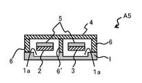
- FIG. 8 is a cross-sectional view that shows a fourth alternative example of the variable capacitor A 1 .
- the plan view of the fourth alternative example is the same as that of FIG. 6 , and, therefore, is omitted, and only the cross-sectional view corresponds to FIG. 7 is shown.
- a variable capacitor A 5 shown in FIG. 8 differs from the variable capacitor A 1 in that the support 6 ′ is provided between the signal line 2 and the ground electrode 3 and the recesses 1 a are provided on the upper face of the substrate 1 .
- the recesses 1 a are respectively provided below portions of the signal line 2 and ground electrode 3 , facing the movable electrode 4 .
- the variable capacitor A 5 has the advantageous effects of both the first alternative example and the third alternative example.
- the dielectric layers 5 are provided on the upper faces of the signal line 2 and ground electrode 3 in the above described first embodiment and its alternative examples.
- the portion of forming the dielectric layer is not limited to on the upper faces of the signal line 2 and ground electrode 3 .
- the dielectric layers 5 may also be provided on the lower face of the movable electrode 4 .
- the dielectric layer 5 may be provided only on the lower face of the movable electrode 4 without providing on the upper faces of the signal line 2 and ground electrode 3 .
- the dielectric layers 5 need not be provided.
- the dielectric layer 5 is provided for only one of the variable capacitors 11 and 12 (see FIG. 3 ) when the capacitance values of the variable capacitors 11 and 12 are differentiated.
- variable capacitor is used in parallel connection; instead, a variable capacitor used in series connection will be described below.
- FIG. 9 is a plan view for illustrating a second embodiment of a variable capacitor and shows a variable capacitor B 1 used in series connection.
- the variable capacitor B 1 differs from the variable capacitor A 1 in that a signal line 2 ′ is provided in place of the ground electrode 3 and in the shape of the signal lines 2 and 2 ′.
- the signal line 2 extends from a vicinity of one end (left side in FIG. 9 ) of the substrate 1 in the long side direction to a portion that faces the movable electrode 4 .
- the signal line 2 ′ extends from a vicinity of the other end (right side in FIG. 9 ) of the substrate 1 in the long side direction to a portion that faces the movable electrode 4 .
- the above configuration is to not produce the parasitic capacitance, while parallel extended portions between signal lines 2 and 2 ′ as shown in FIG. 1 produce a parasitic capacitance.
- FIG. 10 shows an equivalent circuit diagram of the variable capacitor B 1 which is connected to a DC power for driving the variable capacitor B 1 .
- the variable capacitor B 1 is represented by two variable capacitors 11 ′ and 12 ′ connected in series.
- the signal line 2 and the movable electrode 4 form the variable capacitor 11 ′.
- the signal line 2 ′ and the movable electrode 4 form the variable capacitor 12 ′.
- the movable electrode 4 is connected to the DC power 13 through the inductor 14 , which serves as an RF block.
- variable capacitor B 1 differs from the variable capacitor A 1 in that it is used in series connection with a signal line for an RF signal flowing from the signal line 2 to the signal line 2 ′.
- the variable capacitor B 1 has a commonality with the variable capacitor A 1 in that it operates as a capacitive switch by switching a driving voltage applied from the DC power 13 between Voff and Von.
- variable capacitor B 1 is configured so that the two variable capacitors 11 ′ and 12 ′ are connected in series.
- a driving voltage applied from the DC power 13 is blocked by the variable capacitors 11 ′ and 12 ′.
- the variable capacitors 11 ′ and 12 ′ function as a DC block, it is not necessary to provide a capacitor as a DC block, which is necessary when the existing variable capacitor F 1 is used.
- the dielectric layers 5 may also be provided on the lower face of the movable electrode 4 , or may be provided only on the lower face of the movable electrode 4 instead of being provided on the both upper faces of the signal lines 2 and 2 ′.
- the dielectric layers 5 need not be provided when the variable capacitor B 1 is configured so that the movable electrode 4 do not contact the signal line 2 or 2 ′ at an application of a maximal driving voltage.
- the dielectric layer 5 is provided for only one of the variable capacitors 11 ′ and 12 ′ (see FIG. 10 ) when the capacitance values of the variable capacitors 11 ′ and 12 ′ are differentiated, or the like.
- the shape of the signal lines 2 and 2 ′ is not limited to the one described in the second embodiment. If a parasitic capacitance may be ignored, the signal lines 2 and 2 ′ may be extended to near both ends of the substrate 1 in the long side direction.
- the shape of the movable electrode 4 is also not limited to the one described in the second embodiment.
- FIGS. 11 , 12 and 13 are views for illustrating a third embodiment of a variable capacitor.
- FIG. 11 is a plan view of a variable capacitor C 1 ;
- FIG. 12 a cross-sectional view taken along the line XII-XII in FIG. 11 ;
- FIG. 13 a cross-sectional view taken along the line XIII-XIII in FIG. 11 .
- the variable capacitor C 1 differs from the variable capacitor B 1 in the shape of the signal lines 2 and 2 ′ and the shape of a movable electrode 4 ′.
- the signal line 2 is provided parallel to the long side of the substrate 1 at the center in the short side direction so as to extend from a vicinity of one end in the long side direction to a vicinity back from the center.
- the signal line 2 ′ is provided parallel to the long side of the substrate 1 at the center in the short side direction so as to extend from a vicinity of the other end in the long side direction to a vicinity back from the center.
- a predetermined gap is provided between the signal line 2 and the signal line 2 ′ to prevent electrical connection and development of parasitic capacitance.
- the movable electrode 4 ′ forms a substantially rectangle or square shape in plan view and is provided around the center of the substrate 1 .
- the movable electrode 4 ′ is bridged with the pair of supports 6 provided near both ends in the short side direction, and is movable in a vertical direction with respect to the upper face of the substrate 1 .
- the movable electrode 4 ′ has portions facing the signal lines 2 and 2 ′.
- the dielectric layers 5 are provided on the upper faces of the portions of the signal lines 2 and 2 ′, facing the movable electrode 4 ′.
- variable capacitor C 1 Since the variable capacitor C 1 is formed so that only the shape of the signal lines 2 , 2 ′ and movable electrode 4 ′ of the variable capacitor B 1 are modified, the equivalent circuit diagram connected to a DC power for supplying a driving voltage is the same as that of FIG. 10 . Thus, the variable capacitor C 1 also does not need a capacitor, which serves as a DC block. Accordingly the variable capacitor C 1 has the same advantageous effect as that of the variable capacitor B 1 That is, the size of a device using the variable capacitor C 1 may be reduced.
- FIG. 14 is a plan view that shows a first alternative example of the variable capacitor C 1 . Note that cross-sectional views that correspond to FIGS. 12 and 13 of the variable capacitor C 1 are omitted.
- a variable capacitor C 2 differs from the variable capacitor C 1 in that a pair of ground electrodes 3 ′ are formed so that the signal lines 2 and 2 ′ are placed between the pair of ground electrodes 3 ′.
- the signal lines 2 , 2 ′ and the pair of ground electrodes 3 ′ of the variable capacitor C 2 form a CPW structure. Thus, it is possible to easily adjust the designed impedance of the signal lines 2 and 2 ′ in the variable capacitor C 2 as well.
- FIG. 15 is a cross-sectional view that shows a second alternative example of the variable capacitor C 1 . Note that the plan view that corresponds to FIG. 11 of the variable capacitor C 1 and the cross-sectional view that corresponds to FIG. 12 of the variable capacitor C 1 are omitted.
- a variable capacitor C 3 shown in FIG. 15 differs from the variable capacitor C 1 in that the recess 1 a is provided on the upper face of the substrate 1 . The recess 1 a is provided below portions of the signal lines 2 and 2 ′, facing the movable electrode 4 .
- the portions of the signal lines 2 and 2 ′, facing the movable electrode 4 are movable in a vertical direction (top-bottom direction in FIG. 15 ) with respect to the upper face of the substrate 1 . It is possible to suppress a driving voltage applied to the movable electrode 4 ′ to a lesser magnitude, because the movable electrode 4 , the signal lines 2 and 2 ′ are movable, as in the case of the variable capacitor A 4 shown in FIGS. 6 and 7 .
- the recess 1 a decreases the area in which the signal lines 2 and 2 ′ contact the substrate 1 . Accordingly, electric charge leaking from the signal line 2 or 2 ′ to the substrate 1 may be suppressed. Consequently, it is possible to improve the Q value of the variable capacitor C 3 .
- the recess 1 a is formed as a single large recess, but it is not limited to it.
- a recess 1 a may be provided separately below a portion of the signal line 2 , facing the movable electrode 4 ′, and below a portion of the signal line 2 ′, facing the movable electrode 4 ′.
- a driving voltage applied to the movable electrode 4 ′ may be suppressed to a lesser magnitude by the configuration in which portions of the signal lines 2 and 2 ′, facing the movable electrode 4 ′, are movable in the vertical direction. At this configuration, it is applicable that only one of the portions is movable and the other one is fixed.
- the dielectric layers 5 may also be provided on the lower face of the movable electrode 4 ′, or may be not provided on the upper faces of the signal lines 2 and 2 ′ but provided only on the lower face of the movable electrode 4 ′.
- the dielectric layers 5 need not be provided.
- the capacitance values of the variable capacitor 11 ′ and variable capacitor 12 ′ are differentiated, or the like, it is applicable that the dielectric layer 5 is provided for only one of them and no dielectric layer 5 is provided for the other one.
- each electrode may be the same as those of the third embodiment.
- FIG. 16 is a view for illustrating a fourth embodiment of a variable capacitor according to the invention and is a plan view that shows a variable capacitor D 1 used in parallel connection.
- the variable capacitor D 1 differs from the variable capacitor C 1 in that the ground electrode 3 is provided in place of the signal line 2 ′ and in the shapes of the signal line 2 and the ground electrode 3 .
- the signal line 2 and the ground electrode 3 each have a T-shape in plan view; instead, they may be formed in the same shape as the signal lines 2 and 2 ′ of the variable capacitor C 1 .
- the variable capacitor D 1 is formed so that only the shapes of the signal line 2 , ground electrode 3 and movable electrode 4 of the variable capacitor A 1 are modified. Accordingly, the equivalent circuit diagram connected to a DC power that supplies a driving voltage is the same as that of FIG. 3 . Thus, since a voltage generated on the signal line 2 by an RF signal is divided by the variable capacitors 11 and 12 , voltages applied to both ends of each of the variable capacitors 11 and 12 (a voltage between the movable electrode 4 and the signal line 2 ; and a voltage between the movable electrode 4 and the ground electrode 3 ) are about half the generated voltage. Thus, the variable capacitor D 1 also has the same advantageous effect as that of the variable capacitor A 1 .
- the dielectric layers 5 may also be provided on the lower face of the movable electrode 4 ′, or may be not provided on the upper faces of the signal line 2 and ground electrode 3 but provided only on the lower face of the movable electrode 4 ′.
- the dielectric layers 5 need not be provided.
- the capacitance values of the variable capacitor 11 and variable capacitor 12 see FIG. 3 ) are differentiated, it is applicable that the dielectric layer 5 is provided for only one of them.
- variable capacitor is used as a capacitive switch, but it is not limited to it.
- it When it is configured so that the capacitance smoothly varies in accordance with a change in a driving voltage applied to the movable electrode 4 or 4 ′, it may be used as a variable capacitor that controls the capacitance using the driving voltage.
- FIG. 17 is a plan view that shows a ⁇ matching circuit element E 1 in which an inductor 2 a is provided in the signal line 2 of the variable capacitor A 3 shown in FIG. 5 .
- FIG. 18 shows an equivalent circuit diagram which shows the ⁇ matching circuit element E 1 and a DC power for supplying a driving voltage to the ⁇ matching circuit element E 1 .
- FIG. 19 is a plan view that shows a ⁇ matching circuit element E 2 in which a movable electrode 4 is further added to the variable capacitor A 3 shown in FIG. 5 and an inductor 2 a is provided in the signal line 2 at a position between the two movable electrodes 4 .
- FIG. 20 shows an equivalent circuit diagram which shows a DC power for supplying a driving voltage and the ⁇ matching circuit element E 2 connected to the DC power.
- FIG. 21 is a plan view that shows a ⁇ matching circuit element E 3 in which an inductor 2 a is provided in the signal line 2 of the variable capacitor D 1 shown in FIG. 16 .
- the equivalent circuit diagram which shows a DC power for supplying a driving voltage to the ⁇ matching circuit element E 3 and the ⁇ matching circuit element E 3 connected to the DC power is the same as that of FIG. 18 .
- FIG. 22 is a plan view that shows a ⁇ matching circuit element E 4 in which a movable electrode 4 ′ is further added to the variable capacitor D 1 shown in FIG. 16 and an inductor 2 a is provided in the signal line 2 at a position between the two movable electrodes 4 ′.
- the equivalent circuit diagram when a DC power that supplies a driving voltage to the ⁇ matching circuit element E 4 is the same as that of FIG. 20 .
- These matching circuit elements employ the variable capacitor according to the above described first embodiment or fourth embodiment. Accordingly, it is possible to set a driving voltage to a lesser magnitude as compared with the existing matching circuit element, and it is possible to keep reliability. In addition, these matching circuit elements may be reduced in size as compared with the existing matching circuit element.
- FIG. 23 is a plan view that shows a ⁇ matching circuit element F 1 in which an inductor 2 a is provided between the signal line 2 and ground electrode 3 ′ of the variable capacitor C 2 shown in FIG. 14 .
- FIG. 24 shows an equivalent circuit diagram which includes a DC power for supplying a driving voltage to the ⁇ matching circuit element F 1 and the ⁇ matching circuit element F 1 connected to the DC power.
- FIG. 25 is a plan view that shows a ⁇ matching circuit element F 2 in which an inductor 2 a and an inductor 2 ′ a are respectively provided between the signal line 2 and ground electrode 3 ′ and between the signal line 2 ′ and ground electrode 3 ′ of the variable capacitor C 2 shown in FIG. 14 .
- FIG. 26 shows an equivalent circuit diagram which includes a DC power for supplying a driving voltage to the ⁇ matching circuit element F 2 and the ⁇ matching circuit element F 2 connected to the DC power.
- the size may be reduced as compared with the existing matching circuit element.
- variable capacitor and matching circuit element according to the embodiments may be used as an electronic component of a mobile terminal apparatus.
- FIG. 27 is a block diagram that shows a front end portion of a mobile terminal apparatus in which the variable capacitors and matching circuit elements according to the embodiments are used as electronic components.
- the front end portion G 1 of the mobile terminal apparatus includes an adaptive array antenna G 101 that uses a phaser, a tunable filter G 102 , a duplexer G 104 , impedance matching circuits G 103 , G 105 and G 107 , amplifiers G 106 and G 108 each having a matching circuit, and a variable frequency oscillator G 109 formed of a Voltage Controlled Oscillator (VCO).
- VCO Voltage Controlled Oscillator
- an RF signal (receiving signal) of a specific receiving band is extracted by the tunable filter G 102 from an RF signal received by the adaptive array antenna G 101 , and is input to the amplifier G 108 by the duplexer G 104 .
- the receiving signal is amplified in the amplifier G 108 , then mixed with a local signal output from the variable frequency oscillator G 109 and converted to a predetermined intermediate frequency. Then, the converted signal is output to a receiving portion (not shown).
- an RF signal (transmitting signal) input from a transmitting portion (not shown) is amplified by the amplifier G 106 and then input to the tunable filter G 102 through the duplexer G 104 .
- the transmitting signal is radiated from the adaptive array antenna G 101 after frequencies outside a specific transmitting band is removed by the tunable filter G 102 .
- the configurations and functions of the components G 101 to G 109 are typical, and therefore description thereof is omitted.
- the variable capacitor according to the embodiments is used as an element for varying the frequency of the tunable filter G 102 and the frequency of the variable frequency oscillator G 109 in the front end portion G 1 of the mobile terminal apparatus shown in FIG. 27 .
- the matching circuit element according to the embodiments is used as the phaser of the adaptive array antenna G 101 , the impedance matching circuits G 103 , G 105 and G 107 and the matching circuits of the amplifiers G 106 and G 108 .
- the front end portion G 1 to be smaller than that using the existing variable capacitor and matching circuit element, it is possible to reduce the size of a mobile terminal apparatus.
- variable capacitor and the matching circuit element according to the invention may also have the same advantageous effect.
- variable capacitor, matching circuit element and mobile terminal apparatus are not limited to the above described embodiments.
- the specific configuration of each component of the variable capacitor, matching circuit element and mobile terminal apparatus may be variously changed in design.
Landscapes
- Engineering & Computer Science (AREA)
- Power Engineering (AREA)
- Microelectronics & Electronic Packaging (AREA)
- Micromachines (AREA)
- Semiconductor Integrated Circuits (AREA)
Applications Claiming Priority (2)
| Application Number | Priority Date | Filing Date | Title |
|---|---|---|---|
| JP2008-038808 | 2008-02-20 | ||
| JP2008038808A JP5363005B2 (ja) | 2008-02-20 | 2008-02-20 | 可変容量素子、整合回路素子、および携帯端末装置 |
Publications (2)
| Publication Number | Publication Date |
|---|---|
| US20090207549A1 US20090207549A1 (en) | 2009-08-20 |
| US8665579B2 true US8665579B2 (en) | 2014-03-04 |
Family
ID=40561903
Family Applications (1)
| Application Number | Title | Priority Date | Filing Date |
|---|---|---|---|
| US12/366,417 Expired - Fee Related US8665579B2 (en) | 2008-02-20 | 2009-02-05 | Variable capacitor, matching circuit element, and mobile terminal apparatus |
Country Status (5)
| Country | Link |
|---|---|
| US (1) | US8665579B2 (fr) |
| EP (1) | EP2093778B1 (fr) |
| JP (1) | JP5363005B2 (fr) |
| KR (1) | KR101041326B1 (fr) |
| CN (1) | CN101515503B (fr) |
Cited By (2)
| Publication number | Priority date | Publication date | Assignee | Title |
|---|---|---|---|---|
| US20130286534A1 (en) * | 2012-04-27 | 2013-10-31 | Kabushiki Kaisha Toshiba | Variable-capacitor device and driving method thereof |
| US20160268675A1 (en) * | 2013-11-28 | 2016-09-15 | Murata Manufacturing Co., Ltd. | Front end circuit and wireless communication device |
Families Citing this family (11)
| Publication number | Priority date | Publication date | Assignee | Title |
|---|---|---|---|---|
| JP2009212168A (ja) * | 2008-02-29 | 2009-09-17 | Sony Corp | 可変容量素子、可変容量素子の調整方法、可変容量デバイス、及び電子機器 |
| JP5204066B2 (ja) * | 2009-09-16 | 2013-06-05 | 株式会社東芝 | Memsデバイス |
| JP5338615B2 (ja) * | 2009-10-27 | 2013-11-13 | 富士通株式会社 | 可変容量デバイスおよび可変容量素子の駆動方法 |
| WO2011092980A1 (fr) * | 2010-01-28 | 2011-08-04 | 株式会社村田製作所 | Dispositif à capacitance variable |
| KR101104537B1 (ko) * | 2010-05-28 | 2012-01-11 | 한국과학기술원 | 가변 캐패시터 및 그의 구동 방법 |
| KR101744979B1 (ko) | 2010-11-25 | 2017-06-20 | 엘지이노텍 주식회사 | 멤스를 이용한 튜너 모듈 |
| JP5805786B2 (ja) * | 2011-11-28 | 2015-11-10 | 京セラ株式会社 | 無線通信システム、無線通信システムの制御方法、及び基地局 |
| WO2014038086A1 (fr) | 2012-09-10 | 2014-03-13 | 富士通株式会社 | Circuit à capacité variable et circuit d'adaptation d'impédance |
| EP2725595A1 (fr) * | 2012-10-25 | 2014-04-30 | Delfmems | Condensateur fixe MEMS comprenant un espace contenant un gaz et procédé de fabrication dudit condensateur |
| GB2558307B (en) * | 2016-12-30 | 2021-05-05 | Lumentum Tech Uk Limited | Waveguide array |
| US12124150B2 (en) * | 2021-05-25 | 2024-10-22 | Keysight Technologies, Inc. | Radio frequency (RF) phase velocity tuner for setting an electrooptic (EO) modulator bandwidth at different optical wavelengths |
Citations (22)
| Publication number | Priority date | Publication date | Assignee | Title |
|---|---|---|---|---|
| EP0986077A2 (fr) | 1998-09-12 | 2000-03-15 | Lucent Technologies Inc. | Article comprenant un condensateur variable multiport |
| US6215644B1 (en) | 1999-09-09 | 2001-04-10 | Jds Uniphase Inc. | High frequency tunable capacitors |
| DE10043758A1 (de) | 1999-12-15 | 2001-07-05 | Fraunhofer Ges Forschung | Durchstimmbarer Hochfrequenzkondensator |
| JP2002250665A (ja) | 2001-02-23 | 2002-09-06 | Omron Corp | 静電容量式センサ及びその製造方法 |
| US20030223176A1 (en) | 2002-03-08 | 2003-12-04 | Yasutaka Fujii | Variable capacitance element |
| JP2004074341A (ja) | 2002-08-15 | 2004-03-11 | Murata Mfg Co Ltd | 半導体装置 |
| US6750742B2 (en) * | 2002-11-01 | 2004-06-15 | Electronics And Telecommunications Research Institute | Radio frequency device using micro-electronic-mechanical system technology |
| US20040113727A1 (en) | 2002-12-12 | 2004-06-17 | Murata Manufacturing Co., Ltd. | RF-mems switch |
| KR20050023144A (ko) | 2003-08-27 | 2005-03-09 | 한국전자통신연구원 | 정전식 양방향 미세기전 액추에이터 |
| JP2005197997A (ja) | 2004-01-07 | 2005-07-21 | Sharp Corp | 電圧制御発振器並びにそれを用いた高周波受信器及び高周波送信器 |
| US20060086597A1 (en) | 2004-10-21 | 2006-04-27 | Electronics And Telecommunications Research Institude | Micro-electromechanical systems switch and method of fabricating the same |
| JP2006165380A (ja) | 2004-12-09 | 2006-06-22 | Kyocera Corp | 可変容量コンデンサ |
| JP2006210843A (ja) | 2005-01-31 | 2006-08-10 | Fujitsu Ltd | 可変キャパシタ及びその製造方法 |
| JP2006228717A (ja) | 2005-01-21 | 2006-08-31 | Matsushita Electric Ind Co Ltd | 電気機械スイッチ |
| US20060226735A1 (en) | 2005-04-11 | 2006-10-12 | Kabushiki Kaisha Toshiba | Semiconductor device formed by using MEMS technique |
| US7232699B1 (en) | 2003-05-28 | 2007-06-19 | United States Of America As Represented By The Secretary Of The Navy | Method of making a high precision microelectromechanical capacitor with programmable voltage source |
| US20070183116A1 (en) | 2006-01-24 | 2007-08-09 | Stmicroelectronics S.R.L. | Micro-electro-mechanical variable capacitor for radio frequency applications with reduced influence of a surface roughness |
| US20070206340A1 (en) | 2006-03-06 | 2007-09-06 | Fujitsu Limited | Variable capacitor and method of making the same |
| JP2007274932A (ja) | 2006-04-04 | 2007-10-25 | Kobe Univ | 糖・脂質代謝能の改善剤、およびそのスクリーニング方法 |
| WO2007138102A1 (fr) | 2006-05-31 | 2007-12-06 | Thales | Structure de micro-commutateurs radiofrequence ou hyperfrequence et procede de fabrication d'une telle structure |
| US20080180872A1 (en) | 2007-01-24 | 2008-07-31 | Fujitsu Limited | Drive control method and unit for micro machine device |
| US7446994B2 (en) * | 2004-05-31 | 2008-11-04 | Fujitsu Limited | Variable capacitor and manufacturing method thereof |
Family Cites Families (1)
| Publication number | Priority date | Publication date | Assignee | Title |
|---|---|---|---|---|
| JP2008038808A (ja) | 2006-08-08 | 2008-02-21 | Fuji Heavy Ind Ltd | 蒸発燃料処理装置 |
-
2008
- 2008-02-20 JP JP2008038808A patent/JP5363005B2/ja not_active Expired - Fee Related
-
2009
- 2009-02-04 EP EP09152019.7A patent/EP2093778B1/fr not_active Ceased
- 2009-02-05 US US12/366,417 patent/US8665579B2/en not_active Expired - Fee Related
- 2009-02-19 KR KR1020090013902A patent/KR101041326B1/ko not_active Expired - Fee Related
- 2009-02-20 CN CN2009100076669A patent/CN101515503B/zh not_active Expired - Fee Related
Patent Citations (31)
| Publication number | Priority date | Publication date | Assignee | Title |
|---|---|---|---|---|
| EP0986077A2 (fr) | 1998-09-12 | 2000-03-15 | Lucent Technologies Inc. | Article comprenant un condensateur variable multiport |
| US6242989B1 (en) | 1998-09-12 | 2001-06-05 | Agere Systems Guardian Corp. | Article comprising a multi-port variable capacitor |
| US6215644B1 (en) | 1999-09-09 | 2001-04-10 | Jds Uniphase Inc. | High frequency tunable capacitors |
| US20030099082A1 (en) | 1999-12-15 | 2003-05-29 | Xihe Tuo | Tunable high-frequency capacitor |
| CN1409865A (zh) | 1999-12-15 | 2003-04-09 | 弗兰霍菲尔运输应用研究公司 | 可调高频电容器 |
| DE10043758A1 (de) | 1999-12-15 | 2001-07-05 | Fraunhofer Ges Forschung | Durchstimmbarer Hochfrequenzkondensator |
| JP2003527746A (ja) | 1999-12-15 | 2003-09-16 | フラウンホーファー−ゲゼルシャフト・ツール・フェルデルング・デル・アンゲヴァンテン・フォルシュング・アインゲトラーゲネル・フェライン | 同調可能な高周波コンデンサ |
| JP2002250665A (ja) | 2001-02-23 | 2002-09-06 | Omron Corp | 静電容量式センサ及びその製造方法 |
| US20030223176A1 (en) | 2002-03-08 | 2003-12-04 | Yasutaka Fujii | Variable capacitance element |
| JP2004074341A (ja) | 2002-08-15 | 2004-03-11 | Murata Mfg Co Ltd | 半導体装置 |
| US6750742B2 (en) * | 2002-11-01 | 2004-06-15 | Electronics And Telecommunications Research Institute | Radio frequency device using micro-electronic-mechanical system technology |
| US20040113727A1 (en) | 2002-12-12 | 2004-06-17 | Murata Manufacturing Co., Ltd. | RF-mems switch |
| KR20040051512A (ko) | 2002-12-12 | 2004-06-18 | 가부시키가이샤 무라타 세이사쿠쇼 | Rf-mems 스위치 |
| US7232699B1 (en) | 2003-05-28 | 2007-06-19 | United States Of America As Represented By The Secretary Of The Navy | Method of making a high precision microelectromechanical capacitor with programmable voltage source |
| KR20050023144A (ko) | 2003-08-27 | 2005-03-09 | 한국전자통신연구원 | 정전식 양방향 미세기전 액추에이터 |
| JP2005197997A (ja) | 2004-01-07 | 2005-07-21 | Sharp Corp | 電圧制御発振器並びにそれを用いた高周波受信器及び高周波送信器 |
| US7446994B2 (en) * | 2004-05-31 | 2008-11-04 | Fujitsu Limited | Variable capacitor and manufacturing method thereof |
| US7283025B2 (en) * | 2004-10-21 | 2007-10-16 | Electronics And Telecommunications Research Institute | Micro-electromechanical systems switch and method of fabricating the same |
| US20060086597A1 (en) | 2004-10-21 | 2006-04-27 | Electronics And Telecommunications Research Institude | Micro-electromechanical systems switch and method of fabricating the same |
| JP2006165380A (ja) | 2004-12-09 | 2006-06-22 | Kyocera Corp | 可変容量コンデンサ |
| JP2006228717A (ja) | 2005-01-21 | 2006-08-31 | Matsushita Electric Ind Co Ltd | 電気機械スイッチ |
| JP2006210843A (ja) | 2005-01-31 | 2006-08-10 | Fujitsu Ltd | 可変キャパシタ及びその製造方法 |
| US20070039147A1 (en) | 2005-01-31 | 2007-02-22 | Fujitsu Limited | Variable capacitor and method of manufacturing variable capacitor |
| US20060226735A1 (en) | 2005-04-11 | 2006-10-12 | Kabushiki Kaisha Toshiba | Semiconductor device formed by using MEMS technique |
| US20070183116A1 (en) | 2006-01-24 | 2007-08-09 | Stmicroelectronics S.R.L. | Micro-electro-mechanical variable capacitor for radio frequency applications with reduced influence of a surface roughness |
| US20070206340A1 (en) | 2006-03-06 | 2007-09-06 | Fujitsu Limited | Variable capacitor and method of making the same |
| JP2007274932A (ja) | 2006-04-04 | 2007-10-25 | Kobe Univ | 糖・脂質代謝能の改善剤、およびそのスクリーニング方法 |
| WO2007138102A1 (fr) | 2006-05-31 | 2007-12-06 | Thales | Structure de micro-commutateurs radiofrequence ou hyperfrequence et procede de fabrication d'une telle structure |
| FR2901781A1 (fr) | 2006-05-31 | 2007-12-07 | Thales Sa | Structure de micro-commutateurs radiofrequence ou hyperfrequence et procede de fabrication d'une telle structure |
| US20080180872A1 (en) | 2007-01-24 | 2008-07-31 | Fujitsu Limited | Drive control method and unit for micro machine device |
| JP2008181725A (ja) | 2007-01-24 | 2008-08-07 | Fujitsu Ltd | マイクロマシンデバイスの駆動制御方法および装置 |
Non-Patent Citations (5)
| Title |
|---|
| Chinese Office Action dated Aug. 4, 2011, issued in corresponding Chinese Patent Application No. 200910007666.9. |
| Chinese Office Action dated Dec. 27, 2010, issued in corresponding Chinese Patent Application No. 2009-10007666.9. |
| European Search Report dated Jun. 10, 2009, issued in corresponding European Patent Application No. 09152019.7. |
| Japanese Office Action dated Jul. 17, 2012, issued in corresponding Japanese Patent Application No. 2008-038808, (7 pages). With English Translation. |
| Korean Office Action date Nov. 17, 2010, issued in corresponding Korean Pateant Application No. 10-2009-0013902. |
Cited By (3)
| Publication number | Priority date | Publication date | Assignee | Title |
|---|---|---|---|---|
| US20130286534A1 (en) * | 2012-04-27 | 2013-10-31 | Kabushiki Kaisha Toshiba | Variable-capacitor device and driving method thereof |
| US20160268675A1 (en) * | 2013-11-28 | 2016-09-15 | Murata Manufacturing Co., Ltd. | Front end circuit and wireless communication device |
| US9899734B2 (en) * | 2013-11-28 | 2018-02-20 | Murata Manufacturing Co., Ltd. | Front end circuit and wireless communication device |
Also Published As
| Publication number | Publication date |
|---|---|
| KR101041326B1 (ko) | 2011-06-14 |
| JP2009200157A (ja) | 2009-09-03 |
| JP5363005B2 (ja) | 2013-12-11 |
| EP2093778B1 (fr) | 2016-12-21 |
| EP2093778A1 (fr) | 2009-08-26 |
| US20090207549A1 (en) | 2009-08-20 |
| KR20090090283A (ko) | 2009-08-25 |
| CN101515503A (zh) | 2009-08-26 |
| CN101515503B (zh) | 2013-07-31 |
Similar Documents
| Publication | Publication Date | Title |
|---|---|---|
| US8665579B2 (en) | Variable capacitor, matching circuit element, and mobile terminal apparatus | |
| KR100312364B1 (ko) | 동조형 슬롯안테나 | |
| US6737930B2 (en) | Tunable planar capacitor | |
| US6853534B2 (en) | Tunable capacitor | |
| US6804107B2 (en) | Tunable high-frequency capacitor | |
| CN101438366B (zh) | 微机电系统(mems)可变电容器、激励部件及相关方法 | |
| US6373007B1 (en) | Series and shunt mems RF switch | |
| SE523202C2 (sv) | Chipantenn samt antennanordning och apparat för mobilkommunikation innefattande en sådan chipantenn | |
| JP4188316B2 (ja) | 電子デバイスおよびそのインピーダンス整合方法 | |
| EP2104178A1 (fr) | Module d'antenne et dispositif de communication sans fil | |
| JP4705976B2 (ja) | アンテナ装置 | |
| JP2003258502A (ja) | Rfmems素子 | |
| US7489004B2 (en) | Micro-electro-mechanical variable capacitor for radio frequency applications with reduced influence of a surface roughness | |
| US8363381B2 (en) | Variable capacitive element, variable capacitive device, and method for driving the variable capacitive element | |
| US7102472B1 (en) | MEMS device | |
| US6806788B1 (en) | Micromachine switch | |
| US9325052B2 (en) | Tunable cavity resonator having a post and variable capacitive coupling | |
| US20080315362A1 (en) | Micro-Electro-Mechanical System Varactor | |
| JP2008258670A (ja) | アンテナ装置及び携帯端末 | |
| US20060168788A1 (en) | Method for designing a micro electromechanical device with reduced self-actuation | |
| US20100315757A1 (en) | Electrical component | |
| US6784769B1 (en) | Micro machine switch | |
| JP5752803B2 (ja) | Rf装置およびrf装置のチューニング方法 | |
| US20130241665A1 (en) | Variable capacitor, impedance matching device, mobile terminal thereof and method for matching impedance | |
| JP3608379B2 (ja) | 同調型スロットアンテナ |
Legal Events
| Date | Code | Title | Description |
|---|---|---|---|
| AS | Assignment |
Owner name: FUJITSU LIMITED, JAPAN Free format text: ASSIGNMENT OF ASSIGNORS INTEREST;ASSIGNORS:SHIMANOUCHI, TAKEAKI;IMAI, MASAHIKO;MI, XIAOYU;AND OTHERS;REEL/FRAME:022263/0462;SIGNING DATES FROM 20081216 TO 20081217 Owner name: FUJITSU LIMITED, JAPAN Free format text: ASSIGNMENT OF ASSIGNORS INTEREST;ASSIGNORS:SHIMANOUCHI, TAKEAKI;IMAI, MASAHIKO;MI, XIAOYU;AND OTHERS;SIGNING DATES FROM 20081216 TO 20081217;REEL/FRAME:022263/0462 |
|
| STCF | Information on status: patent grant |
Free format text: PATENTED CASE |
|
| FEPP | Fee payment procedure |
Free format text: PAYOR NUMBER ASSIGNED (ORIGINAL EVENT CODE: ASPN); ENTITY STATUS OF PATENT OWNER: LARGE ENTITY |
|
| MAFP | Maintenance fee payment |
Free format text: PAYMENT OF MAINTENANCE FEE, 4TH YEAR, LARGE ENTITY (ORIGINAL EVENT CODE: M1551) Year of fee payment: 4 |
|
| FEPP | Fee payment procedure |
Free format text: MAINTENANCE FEE REMINDER MAILED (ORIGINAL EVENT CODE: REM.); ENTITY STATUS OF PATENT OWNER: LARGE ENTITY |
|
| LAPS | Lapse for failure to pay maintenance fees |
Free format text: PATENT EXPIRED FOR FAILURE TO PAY MAINTENANCE FEES (ORIGINAL EVENT CODE: EXP.); ENTITY STATUS OF PATENT OWNER: LARGE ENTITY |
|
| STCH | Information on status: patent discontinuation |
Free format text: PATENT EXPIRED DUE TO NONPAYMENT OF MAINTENANCE FEES UNDER 37 CFR 1.362 |
|
| FP | Lapsed due to failure to pay maintenance fee |
Effective date: 20220304 |