US8856482B2 - Systems, devices, memory controllers, and methods for memory initialization - Google Patents
Systems, devices, memory controllers, and methods for memory initialization Download PDFInfo
- Publication number
- US8856482B2 US8856482B2 US13/046,446 US201113046446A US8856482B2 US 8856482 B2 US8856482 B2 US 8856482B2 US 201113046446 A US201113046446 A US 201113046446A US 8856482 B2 US8856482 B2 US 8856482B2
- Authority
- US
- United States
- Prior art keywords
- memory
- memory devices
- devices
- volume address
- controller
- Prior art date
- Legal status (The legal status is an assumption and is not a legal conclusion. Google has not performed a legal analysis and makes no representation as to the accuracy of the status listed.)
- Active, expires
Links
Images


Classifications
-
- G—PHYSICS
- G06—COMPUTING OR CALCULATING; COUNTING
- G06F—ELECTRIC DIGITAL DATA PROCESSING
- G06F13/00—Interconnection of, or transfer of information or other signals between, memories, input/output devices or central processing units
- G06F13/14—Handling requests for interconnection or transfer
- G06F13/16—Handling requests for interconnection or transfer for access to memory bus
-
- G—PHYSICS
- G06—COMPUTING OR CALCULATING; COUNTING
- G06F—ELECTRIC DIGITAL DATA PROCESSING
- G06F12/00—Accessing, addressing or allocating within memory systems or architectures
- G06F12/02—Addressing or allocation; Relocation
- G06F12/06—Addressing a physical block of locations, e.g. base addressing, module addressing, memory dedication
- G06F12/0646—Configuration or reconfiguration
- G06F12/0653—Configuration or reconfiguration with centralised address assignment
-
- G—PHYSICS
- G06—COMPUTING OR CALCULATING; COUNTING
- G06F—ELECTRIC DIGITAL DATA PROCESSING
- G06F12/00—Accessing, addressing or allocating within memory systems or architectures
-
- G—PHYSICS
- G06—COMPUTING OR CALCULATING; COUNTING
- G06F—ELECTRIC DIGITAL DATA PROCESSING
- G06F12/00—Accessing, addressing or allocating within memory systems or architectures
- G06F12/02—Addressing or allocation; Relocation
- G06F12/06—Addressing a physical block of locations, e.g. base addressing, module addressing, memory dedication
- G06F12/0646—Configuration or reconfiguration
- G06F12/0653—Configuration or reconfiguration with centralised address assignment
- G06F12/0661—Configuration or reconfiguration with centralised address assignment and decentralised selection
-
- G—PHYSICS
- G06—COMPUTING OR CALCULATING; COUNTING
- G06F—ELECTRIC DIGITAL DATA PROCESSING
- G06F12/00—Accessing, addressing or allocating within memory systems or architectures
- G06F12/02—Addressing or allocation; Relocation
- G06F12/08—Addressing or allocation; Relocation in hierarchically structured memory systems, e.g. virtual memory systems
- G06F12/0802—Addressing of a memory level in which the access to the desired data or data block requires associative addressing means, e.g. caches
- G06F12/0806—Multiuser, multiprocessor or multiprocessing cache systems
- G06F12/0813—Multiuser, multiprocessor or multiprocessing cache systems with a network or matrix configuration
-
- G—PHYSICS
- G06—COMPUTING OR CALCULATING; COUNTING
- G06F—ELECTRIC DIGITAL DATA PROCESSING
- G06F3/00—Input arrangements for transferring data to be processed into a form capable of being handled by the computer; Output arrangements for transferring data from processing unit to output unit, e.g. interface arrangements
- G06F3/06—Digital input from, or digital output to, record carriers, e.g. RAID, emulated record carriers or networked record carriers
- G06F3/0601—Interfaces specially adapted for storage systems
- G06F3/0602—Interfaces specially adapted for storage systems specifically adapted to achieve a particular effect
- G06F3/061—Improving I/O performance
-
- G—PHYSICS
- G06—COMPUTING OR CALCULATING; COUNTING
- G06F—ELECTRIC DIGITAL DATA PROCESSING
- G06F3/00—Input arrangements for transferring data to be processed into a form capable of being handled by the computer; Output arrangements for transferring data from processing unit to output unit, e.g. interface arrangements
- G06F3/06—Digital input from, or digital output to, record carriers, e.g. RAID, emulated record carriers or networked record carriers
- G06F3/0601—Interfaces specially adapted for storage systems
- G06F3/0602—Interfaces specially adapted for storage systems specifically adapted to achieve a particular effect
- G06F3/0626—Reducing size or complexity of storage systems
-
- G—PHYSICS
- G06—COMPUTING OR CALCULATING; COUNTING
- G06F—ELECTRIC DIGITAL DATA PROCESSING
- G06F3/00—Input arrangements for transferring data to be processed into a form capable of being handled by the computer; Output arrangements for transferring data from processing unit to output unit, e.g. interface arrangements
- G06F3/06—Digital input from, or digital output to, record carriers, e.g. RAID, emulated record carriers or networked record carriers
- G06F3/0601—Interfaces specially adapted for storage systems
- G06F3/0628—Interfaces specially adapted for storage systems making use of a particular technique
- G06F3/0629—Configuration or reconfiguration of storage systems
- G06F3/0631—Configuration or reconfiguration of storage systems by allocating resources to storage systems
-
- G—PHYSICS
- G06—COMPUTING OR CALCULATING; COUNTING
- G06F—ELECTRIC DIGITAL DATA PROCESSING
- G06F3/00—Input arrangements for transferring data to be processed into a form capable of being handled by the computer; Output arrangements for transferring data from processing unit to output unit, e.g. interface arrangements
- G06F3/06—Digital input from, or digital output to, record carriers, e.g. RAID, emulated record carriers or networked record carriers
- G06F3/0601—Interfaces specially adapted for storage systems
- G06F3/0628—Interfaces specially adapted for storage systems making use of a particular technique
- G06F3/0629—Configuration or reconfiguration of storage systems
- G06F3/0632—Configuration or reconfiguration of storage systems by initialisation or re-initialisation of storage systems
-
- G—PHYSICS
- G06—COMPUTING OR CALCULATING; COUNTING
- G06F—ELECTRIC DIGITAL DATA PROCESSING
- G06F3/00—Input arrangements for transferring data to be processed into a form capable of being handled by the computer; Output arrangements for transferring data from processing unit to output unit, e.g. interface arrangements
- G06F3/06—Digital input from, or digital output to, record carriers, e.g. RAID, emulated record carriers or networked record carriers
- G06F3/0601—Interfaces specially adapted for storage systems
- G06F3/0668—Interfaces specially adapted for storage systems adopting a particular infrastructure
- G06F3/0671—In-line storage system
- G06F3/0683—Plurality of storage devices
- G06F3/0688—Non-volatile semiconductor memory arrays
-
- G—PHYSICS
- G11—INFORMATION STORAGE
- G11C—STATIC STORES
- G11C7/00—Arrangements for writing information into, or reading information out from, a digital store
- G11C7/20—Memory cell initialisation circuits, e.g. when powering up or down, memory clear, latent image memory
-
- G—PHYSICS
- G06—COMPUTING OR CALCULATING; COUNTING
- G06F—ELECTRIC DIGITAL DATA PROCESSING
- G06F3/00—Input arrangements for transferring data to be processed into a form capable of being handled by the computer; Output arrangements for transferring data from processing unit to output unit, e.g. interface arrangements
- G06F3/06—Digital input from, or digital output to, record carriers, e.g. RAID, emulated record carriers or networked record carriers
- G06F3/0601—Interfaces specially adapted for storage systems
- G06F3/0628—Interfaces specially adapted for storage systems making use of a particular technique
- G06F3/0655—Vertical data movement, i.e. input-output transfer; data movement between one or more hosts and one or more storage devices
- G06F3/0658—Controller construction arrangements
Definitions
- the present disclosure relates generally to semiconductor memory systems, devices, and methods, and more particularly, to systems, devices, memory controllers, and methods for memory initialization.
- Memory devices are typically provided as internal, semiconductor, integrated circuits in computers or other electronic devices. There are many different types of memory including volatile and non-volatile memory. Volatile memory can require power to maintain its information and includes random-access memory (RAM), dynamic random access memory (DRAM), and synchronous dynamic random access memory (SDRAM), among others. Non-volatile memory can provide persistent information by retaining stored information when not powered and can include NAND flash memory, NOR flash memory, read only memory (ROM), Electrically Erasable Programmable ROM (EEPROM), Erasable Programmable ROM (EPROM), phase change random access memory (PCRAM), resistive random access memory (RRAM), and magnetic random access memory (MRAM), such as spin torque transfer random access memory (STT RAM), among others.
- RAM random-access memory
- DRAM dynamic random access memory
- SDRAM synchronous dynamic random access memory
- Non-volatile memory can provide persistent information by retaining stored information when not powered and can include NAND flash memory, NOR flash memory, read only memory (ROM), Electrically Eras
- Memory devices can be combined together to form a memory system such as a solid state drive (SSD), a portable memory drive (e.g., a flash drive), etc.
- a memory system can include non-volatile memory (e.g., NAND flash memory and NOR flash memory), and/or can include volatile memory (e.g., DRAM and SRAM), among various other types of non-volatile and volatile memory.
- non-volatile memory e.g., NAND flash memory and NOR flash memory
- volatile memory e.g., DRAM and SRAM
- an SSD can be used to replace hard disk drives as the main storage device for a computer, as the solid state drive can have advantages over hard drives in terms of performance, size, weight, ruggedness, operating temperature range, and power consumption.
- SSDs can have superior performance when compared to magnetic disk drives due to their lack of moving parts, which may avoid seek time, latency, and other electro-mechanical delays associated with magnetic disk drives.
- SSD manufacturers can use non-volatile flash memory to create flash SSDs that may not use an internal battery supply, thus allowing the drive to be more versatile and compact.
- a memory system can include a number of discrete memory devices (e.g., packages), which can be multi-chip packages (MCPs).
- MCPs can include a number of memory dies and/or chips each having a number of memory units associated therewith.
- the memory units can execute commands received from a host, report status to the host, and can include a number of memory arrays along with peripheral circuitry.
- the memory arrays can include memory cells that can be organized into a number of physical groups (e.g., blocks), with each of the groups capable of storing multiple pages of data.
- multiple memory devices are coupled to a memory controller via a shared bus.
- the memory controller can regulate performance of various operations such as erase operations, program operations, and read operations, for example.
- the interaction between the memory controller and the multiple memory devices can affect various characteristics of a memory system including power consumption, processing speed, and/or data integrity, among other memory system characteristics.
- FIG. 1 is a block diagram of a computing system in accordance with a number of embodiments of the present disclosure.
- FIG. 2 is a block diagram of a portion of a system configured to control memory in accordance with a number of embodiments of the present disclosure.
- FIG. 3 is a block diagram of a portion of a system configured to control memory in accordance with a number of embodiments of the present disclosure.
- FIG. 4 is a block diagram of a portion of a system configured to control memory in accordance with a number of embodiments of the present disclosure.
- FIG. 5 is a flow chart illustrating a method for controlling memory in accordance with a number of embodiments of the present disclosure.
- Initializing memory can include configuring memory devices in parallel.
- the memory devices can receive a shared enable signal.
- a unique volume address can be assigned to each of the memory devices.
- Embodiments of the present disclosure can provide various benefits such as reducing pin counts on memory controllers and/or providing flexibility regarding interaction between a memory controller and memory devices coupled to the memory controller via a shared bus as compared to some previous memory systems, devices, and methods, among other benefits.
- providing flexibility can include allowing a memory controller to control (e.g., initialize), memory devices in parallel or in series, which can allow the memory controller to tradeoff between power use and performance depending on which is more desirable in a particular instance.
- FIG. 1 is a functional block diagram of a computing system 100 in accordance with a number of embodiments of the present disclosure.
- Computing system 100 includes a memory system 104 , for example a number of solid state drives (SSDs), communicatively coupled to a host 102 .
- Memory system 104 can be communicatively coupled to the host 102 through an interface 106 , such as a backplane or bus, for instance.
- interface 106 such as a backplane or bus, for instance.
- Examples of hosts 102 can include laptop computers, personal computers, digital cameras, digital recording and playback devices, mobile telephones, PDAs, memory card readers, and interface hubs, among other host systems.
- the interface 106 can include a serial advanced technology attachment (SATA), peripheral component interconnect express (PCIe), or a universal serial bus (USB), among other connectors and interfaces.
- SATA serial advanced technology attachment
- PCIe peripheral component interconnect express
- USB universal serial bus
- host interface 106 can provide an interface for passing control, address, data, and other signals between the memory system 104 and the host 102 .
- the host 102 can include a number of processors 105 (e.g., parallel processors, co-processors, etc.) communicatively coupled to a memory and bus control 107 .
- the processor 105 can be a number of microprocessors, or some other type of controlling circuitry, such as a number of application-specific integrated circuits (ASICs), for example.
- ASICs application-specific integrated circuits
- Other components of the computing system 100 may also have processors.
- the memory and bus control 107 can have memory and other components directly communicatively coupled thereto, for example, dynamic random access memory (DRAM) 111 , graphic user interface 118 , and/or other user interface (e.g., display monitor, keyboard, mouse, etc.).
- DRAM dynamic random access memory
- the memory and bus control 107 can also have a peripheral and bus control 109 communicatively coupled thereto, which in turn, can connect to a memory system, such as a flash drive 119 using a universal serial bus (USB) interface, for example, a non-volatile memory host control interface (NVMHCI), flash memory 117 , and/or the memory system 104 .
- a memory system such as a flash drive 119 using a universal serial bus (USB) interface, for example, a non-volatile memory host control interface (NVMHCI), flash memory 117 , and/or the memory system 104 .
- USB universal serial bus
- NVMHCI non-volatile memory host control interface
- the memory system 104 can be used in addition to, or in lieu of, a hard disk drive (HDD) in a number of different computing systems.
- HDD hard disk drive
- the computing system 100 illustrated in FIG. 1 is one example of such a system; however, embodiments of the present disclosure are not limited to the configuration shown
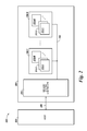
- FIG. 2 is a block diagram of a portion of a system 200 configured to control memory in accordance with a number of embodiments of the present disclosure.
- the system 200 includes a memory system 204 , which can be an SSD, for example.
- the memory system 204 can be coupled to a host 202 via a host interface 206 and can include a memory controller 215 (e.g., memory control circuitry, firmware, and/or software), and a number of memory devices 230 - 1 , . . . , 230 -N coupled to the memory controller 215 .
- the memory controller 215 can be an application specific integrated circuit (ASIC) coupled to a printed circuit board.
- ASIC application specific integrated circuit
- the memory system 204 includes a bus 220 to send/receive various signals (e.g., data signals, control signals, and/or address signals), between the memory devices 230 - 1 , . . . , 230 -N and the memory controller 215 .
- various signals e.g., data signals, control signals, and/or address signals
- FIG. 2 includes a single bus 220
- the memory system 204 can include a separate data bus (DQ bus), control bus, and address bus, in some embodiments.
- the bus 220 is shared by the number of memory devices 230 - 1 , . . .
- bus structures including, but not limited to, bus structures related to Open NAND Flash Interface (ONFI), Compact Flash Interface, Multimedia Card (MMC), Secure Digital (SD), CE-ATA, Industrial Standard Architecture (ISA), Micro-Channel Architecture (MSA), Extended ISA (EISA), Intelligent Drive Electronics (IDE), VESA Local Bus (VLB), Peripheral Component Interconnect (PCI), Card Bus, Universal Serial Bus (USB), Advanced Graphics Port (AGP), Personal Computer Memory Card International Association bus (PCMCIA), Firewire (IEEE 1394), and Small Computer Systems Interface (SCSI).
- ONFI Open NAND Flash Interface
- MMC Compact Flash Interface
- SD Secure Digital
- ISA Industrial Standard Architecture
- MSA Micro-Channel Architecture
- EISA Extended ISA
- IDE Intelligent Drive Electronics
- VLB VESA Local Bus
- PCI Peripheral Component Interconnect
- Card Bus Universal Serial Bus
- USB Universal Serial Bus
- AGP Advanced Graphics Port
- PCMCIA Personal Computer Memory Card International Association bus
- Firewire IEEE 1394
- the memory devices 230 - 1 , . . . , 230 -N can comprise a number of dies and/or chips that can include a number of memory units 212 - 1 , 212 - 2 , . . . , 212 -M providing a storage volume for the memory system 204 .
- the memory units 212 - 1 , 212 - 2 , . . . , 212 -M can be referred to as logical units (LUNs) and can include a number of memory arrays along with peripheral circuitry thereon.
- LUNs logical units
- 212 -M can be the minimum component of memory system 204 capable of independently executing commands from and reporting status to the memory controller 215 and/or host 202 via bus 220 .
- the memory units 212 - 1 , 212 - 2 , . . . , 212 -M can include Flash memory arrays having a NAND architecture, for example. However, embodiments are not limited to a particular type of memory array or array architecture.
- each volume can be a set of memory units that share an enable signal (e.g., a chip enable (CE) signal) received from the memory controller 215 , within one of the memory devices 230 - 1 , . . . , 230 -N.
- an enable signal e.g., a chip enable (CE) signal
- a number of enable inputs and/or outputs (e.g., pins, terminals, etc.) associated with the memory devices 230 - 1 , . . . , 230 -N can be coupled together and may be coupled to one shared enable output (e.g., pin, terminal, etc.) of the memory controller 215 .
- a single chip enable output of the controller may be shared by a number of the memory devices 230 - 1 , . . . , 230 -N, in various embodiments.
- the state of an enable signal can be used to activate and/or deactivate a memory volume, and in some instances, an entire memory device.
- a memory system can be configured such that memory volumes are active low (e.g., the memory volumes can process commands received from the memory controller when their associated chip enable signal is in a low state).
- the memory volumes become inactive (e.g., deselected) and cannot process commands when the chip enable signal they share is in a high state.
- Embodiments of the present disclosure are not limited to memory volumes having a particular chip enable configuration.
- the target volume(s) within the memory devices 230 - 1 , . . . , 230 -N can have volume addresses assigned thereto.
- assigning can refer to, for example, assigning, establishing, and/or setting a volume address.
- the assigned volume addresses can be used to distinguish among target volumes associated with a shared chip enable signal, as described further below.
- FIG. 3 is a block diagram of a portion of a system configured to control memory in accordance with a number of embodiments of the present disclosure.
- the memory system illustrated in FIG. 3 includes a memory controller 315 .
- the memory controller 315 can control access across a number of memory channels.
- the controller 315 includes a number of channel controllers 327 - 1 , 327 - 2 , . . . , 327 -Q each controlling access to a respective memory channel.
- FIG. 3 illustrates separate channel controllers 328 - 1 , 328 - 2 , . . . , 328 -N for each channel, in some embodiments, a channel controller can control more than one channel and/or all channels can be controlled by a single memory controller.
- the memory controller 315 can include a first interface for coupling the memory controller 315 to a host (e.g., host 202 illustrated in FIG. 2 ).
- the memory controller 315 can include a second interface for coupling the memory controller 315 to a plurality of memory devices 330 - 1 , . . . , 330 -N arranged in a linear daisy chain configuration.
- the memory controller 315 can be configured to provide a shared enable signal (e.g., a chip enable signal) to the plurality of memory devices 330 - 1 , . . . , 330 -N during an initialization of the plurality of memory devices 330 - 1 , . . .
- a shared enable signal e.g., a chip enable signal
- the memory controller 315 can be configured to configure the plurality of memory devices 330 - 1 , . . . , 330 -N during the initialization of the plurality of memory devices 330 - 1 , . . . , 330 -N. In some embodiments, the memory controller 315 can be configured to configure the plurality of memory devices 330 - 1 , . . .
- the memory controller 315 can be configured to configure a particular one of the plurality of memory devices 330 - 1 , . . . , 330 -N prior to assigning the unique volume address to the particular one of the plurality of memory devices 330 - 1 , . . . , 330 -N.
- the memory controller 315 is coupled to a number of memory devices 330 - 1 , . . . , 330 -N via a bus 320 (e.g., a shared data, address, and control bus).
- a bus 320 e.g., a shared data, address, and control bus.
- Each of the memory devices 330 - 1 and 330 - 2 includes a number of memory units 312 - 1 , 312 - 2 , 312 - 3 , . . . , 312 -M.
- the memory units 312 - 1 , . . . , 312 -M can be memory die and the memory devices 330 - 1 , . . . , 330 -N can be multi-chip packages, as an example.
- the memory units 312 - 1 , . . . , 312 -M within each memory device are organized (e.g., grouped) into a number of target volumes 313 - 1 , 313 - 2 , 313 - 3 , . . . , 313 -P.
- a group of memory units of a target volume can share a chip enable (CE).
- CE chip enable
- a chip enable can take the form of a pin or another physical contact.
- memory units 312 - 1 and 312 - 2 can be included in target volume 313 - 1 within memory device 330 - 1 .
- the memory controller includes two CE pins 328 - 1 (CE 1 ) and 328 - 2 (CE 2 ) dedicated to providing CE signals to the memory devices 330 - 1 and 330 - 2 .
- CE 1 is coupled to a CE pin associated with target volume 313 - 1 within memory device 330 - 1 and with target volume 313 - 3 within memory device 330 -N
- CE 2 is coupled to a CE pin associated with target volume 313 - 2 within memory device 330 - 1 and with target volume 313 -P within memory device 330 -N.
- the controller 315 and memory devices 330 - 1 , . . . , 330 -N can have various other contacts (e.g., pins) connected via signal lines, for instance, which can be part of bus 320 .
- each of the channel controllers 327 - 1 , . . . , 327 -Q can be coupled to a number of memory devices.
- the memory system can include more or fewer memory devices per channel, more or fewer target volumes per memory device, etc.
- each of the target volumes 313 - 1 , . . . , 313 -P has an assigned volume address associated therewith (e.g., “Volume 1 ,” Volume 2 ,” Volume 3 ,” . . . , “Volume P”).
- a command provided by the controller 315 can assign a volume address to a particular memory device (e.g., to a particular one of the target volumes) to receive a number of later commands from the controller 315 .
- FIG. 4 is a block diagram of a portion of a system configured to control memory in accordance with a number of embodiments of the present disclosure.
- the embodiment illustrated in FIG. 4 includes a number of memory devices 430 - 1 , 430 - 2 , 430 - 3 , . . . , 430 -N and illustrates an example topology for initializing memory in accordance with a number of embodiments of the present disclosure.
- the topology can be a linear daisy chain configuration 440 as illustrated.
- the memory devices 430 - 1 , . . . , 430 -N can be memory devices such as devices 330 - 1 , . . . , 330 -N shown in FIG. 3 .
- the memory devices 430 - 1 , . . . , 430 -N can be NAND memory devices.
- each of the devices 430 - 1 , . . . , 430 -N includes a chain input 439 and a chain output 441 .
- device 430 - 1 includes chain input 439 - 1 (ENi_ 1 ) and chain output 441 - 1 (ENo ⁇ 1 )
- device 430 - 2 includes chain input 439 - 2 (ENi_ 2 ) and chain output 441 - 2 (ENo_ 2 )
- device 430 - 3 includes chain input 439 - 3 (ENi_ 3 ) and chain output 441 - 3 (ENo_ 3 )
- device 430 -N includes chain input 439 -N (ENi_N) and chain output 441 -N (ENo_N).
- the chain inputs 439 and chain outputs 441 of the memory devices 430 - 1 , . . . , 430 -N can be coupled to create a linear daisy chain configuration 440 .
- the chain input 439 - 1 of the first device 430 - 1 in the chain and the chain output 441 -N of the last device 430 -N in the chain are not connected (NC).
- the chain inputs 439 of the other devices are connected to the chain output 441 of the previous device in a linear daisy chain configuration 440 as shown in FIG. 4 .
- each of the memory devices 430 - 1 , . . . , 430 -N include an input to receive a shared enable signal from a memory controller (e.g., memory controller 315 illustrated in FIG. 3 ).
- a memory controller e.g., memory controller 315 illustrated in FIG. 3
- each of the memory devices 430 - 1 , . . . , 430 -N share a common CE pin from the memory controller.
- a chip enable signal 444 (CE 0 _N) from a memory controller is shared by the chip enable pin 438 (CE 1 ) of each of the memory devices 430 - 1 , . . . , 430 -N.
- the CE 1 pin of each of the memory devices 430 - 1 , . . . , 430 -N is associated with (e.g., corresponds to) a particular target volume 413 - 1 , 413 - 2 , 413 - 3 , . . . , 413 -P.
- a target volume can refer to a number of memory units (e.g., LUNs) that share a particular CE signal within a memory device.
- Each of the target volumes can have a volume address (e.g., a unique non-fixed volume address) assigned thereto.
- target volume 413 - 1 is assigned volume address “Volume 1 ”
- target volume 413 - 2 is assigned volume address “Volume 2 ”
- target volume 413 - 3 is assigned volume address “Volume 3 ”
- target volume 413 -P is assigned volume address “Volume P.”
- the volume addresses can be assigned to particular target volumes during initialization (e.g., at power up).
- the states of the chain inputs 439 - 1 , 439 - 2 , 439 - 3 , . . . , 439 -N and of the chip enable pin 438 determines whether the respective memory device 430 - 1 , . . . , 430 -N are able to accept commands. For example, if the chain input 439 of a particular device is high and the CE pin 438 of the device is low, then the particular device can accept commands. If the chain input 439 of the particular device is low or the CE pin 438 is high, then the device cannot accept commands.
- Embodiments are not limited to this example as the combination of states of the chain input 439 and CE pin 438 can be configured differently to allow the device to accept commands.
- a memory controller can provide (e.g., issue) a command indicating a target volume address of a particular target volume to process a number of subsequent commands.
- a volume select command can be provided by the memory controller to the number of memory devices 430 - 1 , . . . , 430 -N (e.g., via a shared bus) in order to select a particular target volume (e.g., 413 - 1 . . . , 413 -P) sharing a particular chip enable signal 444 from the memory controller.
- volume addressing can be used to access particular target volumes of the memory devices 430 - 1 , . . . , 430 -N.
- a chip enable signal (e.g., chip enable signal 444 ) received from a memory controller (e.g., via a shared bus such as shared bus 320 shown in FIG. 3 ) is used to activate a number of memory devices (e.g., 430 - 1 , . . . , 430 -N). For example, assuming the memory devices 430 - 1 , . . . , 430 -N are active low, they can be activated responsive to detecting the chip enable signal 444 switching from a first state to a second state (e.g., from a high to a low state).
- a first state e.g., from a high to a low state
- a command can subsequently be provided to the activated number of memory devices 430 - 1 , . . . , 430 -N.
- the command can indicate (e.g., via a target volume address) a target volume of the number of target volumes (e.g., 413 - 1 . . . , 413 -P) within a particular one of the number of memory devices 430 - 1 , . . . , 430 -N.
- the target volume indicated by the command remains active (e.g., selected) and the remaining target volumes return to their previous states (e.g., their states prior to activation responsive to detecting the switching of the chip enable signal).
- each of the memory devices 430 - 1 , . . . , 430 -N and target volumes 413 - 1 . . . , 413 -P therein return to their previous states.
- a previously selected one of the number of memory volumes e.g., the memory volume which was selected prior to detecting the switching of the enable signal
- those memory volumes which were previously unselected will return to an unselected state.
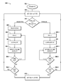
- FIG. 5 is a flow chart illustrating a method 550 for controlling memory in accordance with a number of embodiments of the present disclosure.
- the method 550 can be applied to various memory systems such as those described above in FIGS. 1-4 .
- the method 550 can apply to a number of memory devices coupled to a memory controller via a shared bus.
- the number of memory volumes share a chip enable signal (CE#) from the memory controller and are active low (e.g., the memory volumes activate responsive to detection of a low signal state of the chip enable signal).
- CE# chip enable signal
- the memory volumes can each include a number of memory units (e.g., LUNs) capable of independently executing commands and reporting status to the memory controller.
- volume addresses can be assigned to target volumes.
- a target volume can include a number of memory units sharing a chip enable signal within a memory device (e.g., a package).
- the volume addresses can be assigned to the target volumes during initialization of the system (e.g., at power up).
- the assigned volume addresses can be maintained across reset commands, in a number of embodiments, and different volume addresses can be assigned to the target volumes during a subsequent initialization.
- an initialization can begin at power on, however embodiments are not so limited as initialization can occur without powering on a memory system from a power off state (e.g., a system could be reinitialized without first powering off the memory system).
- a shared enable signal e.g., a shared CE#
- the shared CE# can be set to the first state subsequent to a power up or other memory initialization (including reinitialization) causing event.
- the shared CE# can be coupled to a plurality of memory devices, where the plurality of memory devices are arranged in a linear daisy chain configuration.
- the memory volumes associated with the shared CE# can be configured in parallel or in sequence as indicated at block 556 .
- a memory controller can selectively configure the memory volumes during the initialization in sequence or in parallel, such as by including a programmable option.
- a programmable option can be set either during operation of the memory controller (e.g., during an initialization) or can be set prior to operation of the memory controller (e.g., at fabrication or initial configuration of the memory controller) among others.
- a preliminary command (e.g., a read status command ( 70 h ))
- a read status command can cause retrieval of a status value for the last operation provided.
- Such a command can be accepted by all memory devices regardless of a state of the chain input of the memory devices.
- Some memory systems may require that a memory controller provide such a preliminary command before any other command can be provided.
- a reset command can be provided as indicated at block 560 - 1 .
- the reset command (FFh) can be provided to a first memory device of the plurality of memory devices (e.g., a memory device having a chain input set to a particular state such as a high state). That is, in some embodiments, the reset command may only be accepted by a memory device having a chain input set to the particular state. Thus, providing the reset command can include resetting a particular memory volume in response to the particular memory device having a chain input in the particular state.
- a reset command can put the target memory device in a power up state (e.g., a default power up state).
- the first memory volume can be configured as indicated at block 562 .
- configuring the first memory device can include loading trims on the first memory device.
- Configuring the memory device can include reading and/or writing a device identifier, reading and/or writing device parameters, reading and/or writing device boot code, and/or other configuration actions such that the host can receive and/or provide configuration information from and/or to the memory volume.
- a volume address can be assigned to the first memory volume as indicated at block 564 - 1 .
- a set feature command can be provided to assign a volume address to the first memory volume.
- a volume address can be assigned to each volume in a memory device.
- a particular memory device including two target volumes can have two unique non-fixed volume addresses assigned thereto.
- a chain output of the first memory device can be set to a particular state (e.g., a high state) to deselect the first memory device and/or a target volume associated therewith and cause the chain input of the first memory device to be ignored.
- a state of the chain input of the first memory device can be changed (e.g., to a low state).
- a presence of a next memory device in the chain can be indicated in response to a subsequent query (e.g., a read identification (ID) command) being provided (e.g., to a second memory device) after the first memory device has been deselected.
- a read ID command can identify that a target to which the command was provided supports a particular standard (e.g., the ONFI standard).
- a device supporting the particular standard can return a particular signature indicating the same.
- the device if a device does not support the particular standard, the device will not respond to the read ID command. If a next device responds, then the sequential configuration process can continue as described above for the first memory volume (e.g., as described with respect to blocks 560 - 1 through 566 - 1 ).
- a second memory device can be configured and have a second volume address assigned thereto.
- volume addresses can be unique (e.g., each assigned volume address can be different) and non-fixed (e.g., a particular memory volume can have a different volume address assigned during a subsequent initialization).
- the plurality of memory volumes can be reconfigured and a unique non-fixed volume address can be reassigned to each of the plurality of memory volumes during a subsequent initialization.
- “reassigning” a volume address does not imply that the same volume address is assigned to the same memory volume. Rather, “reassigning” a volume address indicates that a subsequent volume address is assigned to a particular memory volume.
- a particular memory device can be retired, in which case the retired memory device would not have a unique non-fixed volume address assigned thereto during a subsequent initialization, nor would the retired memory device be configured during the subsequent initialization.
- a new memory device can be added to the chain after a previous initialization without the new memory device.
- the plurality of memory devices can be reconfigured and the new memory device can be configured and have unique non-fixed volume addresses assigned thereto.
- the initialization process can be repeated until all of the memory devices have been initialized. For example, subsequent reset commands can be provided sequentially to the remaining memory devices in the chain, the remaining memory devices can be configured sequentially, and different volume addresses can be assigned to the remaining memory devices sequentially.
- next memory device If a next memory device does not respond, then a determination can be made as to whether a next chip enable should be initialized as indicated at block 568 - 1 (e.g., for those memory controllers including more than one CE# such as memory controller 315 illustrated in FIG. 3 ). If another CE# is to be initialized, the process can return to block 554 where the next CE# can be set to the first state for initialization of memory devices and/or volumes associated with the next CE#. After the memory devices and/or volumes associated with a particular CE# have been initialized, the state of the particular CH can be set to a different state (second state) (e.g., a high state), as illustrated at block 570 . Subsequently a volume select command can be provided to select a volume for additional commands (e.g., setting up an on die termination (ODT) matrix), among other commands and/or operations.
- ODT on die termination
- a reset command can be provided to each of the plurality of memory devices as indicated at block 560 - 2 .
- the plurality of memory devices can accept the reset command regardless of a state of a chain input (e.g., high or low) of each of the plurality of memory devices.
- Each of the plurality of memory devices in the chain can be configured in parallel (e.g., substantially simultaneously) in response to the reset command as indicated at block 574 .
- substantially simultaneously at least includes the plurality of memory devices being configured together without the memory controller providing separate commands to configure the plurality of memory devices independently.
- substantially simultaneously can include configuring the plurality of memory devices at the same time. Configuring the memory devices is described in more detail above with respect to block 562 .
- Parallel configuration can be analogous to sequential configuration except that the memory devices are configured substantially simultaneously in parallel rather than individually in sequence.
- a volume address (e.g., a unique non-fixed volume address) can be assigned to each of the memory volumes as indicated at block 564 - 2 .
- Assignment of a volume address according to the parallel configuration process can be analogous to the assignment of a volume address according to the sequential configuration process as described above with respect to block 564 - 1 .
- the volume addresses can be assigned sequentially to each of the plurality of memory devices.
- a chain output of the first memory device can be driven to a particular state (e.g., a high state) to deselect the first memory device and ignore a state of the chain input of the first memory device.
- a first volume address can be assigned to a first memory volume and then a determination can be made as to whether a next device exists in the chain for assignment of a next volume address as indicated at block 566 - 2 .
- a presence of a next memory device in the chain can be indicated in response to a subsequent query (e.g., a read ID command) being provided (e.g., to a second memory device) after the first memory device has been deselected.
- a read ID command can identify that a target to which the command was provided supports a particular standard (e.g., the ONFI standard).
- a device supporting the particular standard can return a particular signature indicating the same.
- a device if a device does not support the particular standard, the device will not respond to the read ID command.
- a volume address can be assigned to the next device as indicated at block 564 - 2 .
- a CE# can be set to a different state and thereby deselect each of the plurality of memory devices and/or volumes associated with that CE#.
- a next memory device not responding e.g., in response to there being no more memory devices associated with a particular CE# to be initialized in the chain
- a determination can be made as to whether a next chip enable should be initialized as indicated at block 568 - 2 (e.g., for those memory controllers including more than one CE#, such as memory controller 315 illustrated in FIG. 3 ).
- the process for determining whether a next CE# should be initialized can be analogous to that described above with respect to block 568 - 1 .
- the state of the particular CE# can be set to a different state (second state) (e.g., a high state) as illustrated at block 570 .
- a volume select command (E1h) can be provided to select a volume for additional commands (e.g., setting up an on die termination (ODT) matrix) among other commands and/or operations.
- Initializing memory can include configuring memory devices in parallel.
- the memory devices can receive a shared enable signal.
- a unique volume address can be assigned to each of the memory devices.
Landscapes
- Engineering & Computer Science (AREA)
- Theoretical Computer Science (AREA)
- Physics & Mathematics (AREA)
- General Engineering & Computer Science (AREA)
- General Physics & Mathematics (AREA)
- Human Computer Interaction (AREA)
- Mathematical Physics (AREA)
- Memory System (AREA)
- Techniques For Improving Reliability Of Storages (AREA)
- Logic Circuits (AREA)
- Information Retrieval, Db Structures And Fs Structures Therefor (AREA)
Priority Applications (10)
| Application Number | Priority Date | Filing Date | Title |
|---|---|---|---|
| US13/046,446 US8856482B2 (en) | 2011-03-11 | 2011-03-11 | Systems, devices, memory controllers, and methods for memory initialization |
| CN201280018889.5A CN103502955B (zh) | 2011-03-11 | 2012-03-08 | 系统、装置、存储器控制器以及用于存储器初始化的方法 |
| KR1020137026781A KR101545425B1 (ko) | 2011-03-11 | 2012-03-08 | 메모리 초기화를 위한 시스템, 디바이스, 메모리 제어기, 및 방법 |
| JP2013557865A JP5918279B2 (ja) | 2011-03-11 | 2012-03-08 | メモリ初期化のためのシステム、装置、メモリコントローラ、および方法 |
| EP12757369.9A EP2684131B1 (fr) | 2011-03-11 | 2012-03-08 | Systèmes, dispositifs, contrôleurs de mémoire et procédés d'initialisation de mémoire |
| PCT/US2012/028291 WO2012125406A2 (fr) | 2011-03-11 | 2012-03-08 | Systèmes, dispositifs, contrôleurs de mémoire et procédés d'initialisation de mémoire |
| TW103146132A TWI529533B (zh) | 2011-03-11 | 2012-03-09 | 系統,裝置,記憶體控制器,以及用於記憶體初始化之方法 |
| TW101108159A TWI472926B (zh) | 2011-03-11 | 2012-03-09 | 系統,裝置,記憶體控制器,以及用於記憶體初始化之方法 |
| US14/483,927 US9251068B2 (en) | 2011-03-11 | 2014-09-11 | Systems, devices, memory controllers, and methods for memory initialization |
| JP2015030336A JP5978332B2 (ja) | 2011-03-11 | 2015-02-19 | メモリ初期化のための方法 |
Applications Claiming Priority (1)
| Application Number | Priority Date | Filing Date | Title |
|---|---|---|---|
| US13/046,446 US8856482B2 (en) | 2011-03-11 | 2011-03-11 | Systems, devices, memory controllers, and methods for memory initialization |
Related Child Applications (1)
| Application Number | Title | Priority Date | Filing Date |
|---|---|---|---|
| US14/483,927 Continuation US9251068B2 (en) | 2011-03-11 | 2014-09-11 | Systems, devices, memory controllers, and methods for memory initialization |
Publications (2)
| Publication Number | Publication Date |
|---|---|
| US20120233433A1 US20120233433A1 (en) | 2012-09-13 |
| US8856482B2 true US8856482B2 (en) | 2014-10-07 |
Family
ID=46797137
Family Applications (2)
| Application Number | Title | Priority Date | Filing Date |
|---|---|---|---|
| US13/046,446 Active 2033-02-03 US8856482B2 (en) | 2011-03-11 | 2011-03-11 | Systems, devices, memory controllers, and methods for memory initialization |
| US14/483,927 Active US9251068B2 (en) | 2011-03-11 | 2014-09-11 | Systems, devices, memory controllers, and methods for memory initialization |
Family Applications After (1)
| Application Number | Title | Priority Date | Filing Date |
|---|---|---|---|
| US14/483,927 Active US9251068B2 (en) | 2011-03-11 | 2014-09-11 | Systems, devices, memory controllers, and methods for memory initialization |
Country Status (7)
| Country | Link |
|---|---|
| US (2) | US8856482B2 (fr) |
| EP (1) | EP2684131B1 (fr) |
| JP (2) | JP5918279B2 (fr) |
| KR (1) | KR101545425B1 (fr) |
| CN (1) | CN103502955B (fr) |
| TW (2) | TWI529533B (fr) |
| WO (1) | WO2012125406A2 (fr) |
Cited By (2)
| Publication number | Priority date | Publication date | Assignee | Title |
|---|---|---|---|---|
| US12082340B2 (en) | 2021-09-22 | 2024-09-03 | Kioxia Corporation | Semiconductor device and memory system |
| US12131040B2 (en) | 2021-10-25 | 2024-10-29 | Micron Technology, Inc. | Delay of initialization at memory die |
Families Citing this family (24)
| Publication number | Priority date | Publication date | Assignee | Title |
|---|---|---|---|---|
| US8856482B2 (en) * | 2011-03-11 | 2014-10-07 | Micron Technology, Inc. | Systems, devices, memory controllers, and methods for memory initialization |
| US9239806B2 (en) | 2011-03-11 | 2016-01-19 | Micron Technology, Inc. | Systems, devices, memory controllers, and methods for controlling memory |
| US8463948B1 (en) * | 2011-07-01 | 2013-06-11 | Intel Corporation | Method, apparatus and system for determining an identifier of a volume of memory |
| US9213610B2 (en) | 2013-06-06 | 2015-12-15 | Lenovo Enterprise Solutions (Singapore) Pte. Ltd. | Configurable storage device and adaptive storage device array |
| US9117504B2 (en) | 2013-07-03 | 2015-08-25 | Micron Technology, Inc. | Volume select for affecting a state of a non-selected memory volume |
| US9933980B2 (en) | 2014-02-24 | 2018-04-03 | Toshiba Memory Corporation | NAND raid controller for connection between an SSD controller and multiple non-volatile storage units |
| US20160078939A1 (en) * | 2014-09-11 | 2016-03-17 | Intel Corporation | Appointing semiconductor dice to enable high stacking capability |
| KR20160120004A (ko) * | 2015-04-07 | 2016-10-17 | 삼성전자주식회사 | 시스템 온-칩 및 이를 포함하는 전자 기기 |
| CN106155948B (zh) * | 2015-04-16 | 2019-07-05 | 伊姆西公司 | 用于存储系统的方法、聚合配置引擎、聚合配置工具以及文件系统 |
| US10095437B2 (en) * | 2015-08-03 | 2018-10-09 | Intel Corporation | Memory access control |
| US10057209B2 (en) * | 2016-07-28 | 2018-08-21 | Qualcomm Incorporated | Time-sequenced multi-device address assignment |
| KR102669694B1 (ko) * | 2016-09-28 | 2024-05-28 | 삼성전자주식회사 | 서로 직렬로 연결된 스토리지 장치들 중 애플리케이션 프로세서에 직접 연결되지 않는 스토리지 장치를 리셋시키는 전자 기기 및 그것의 동작 방법 |
| KR102445674B1 (ko) | 2017-12-18 | 2022-09-22 | 삼성전자주식회사 | 선택적으로 메모리를 부팅시키도록 구성되는 램 컨트롤러 및 그 동작 방법 |
| US10817363B2 (en) * | 2018-03-19 | 2020-10-27 | Micron Technology, Inc. | Health characteristics of a memory device |
| KR20200068496A (ko) * | 2018-12-05 | 2020-06-15 | 에스케이하이닉스 주식회사 | 메모리 장치, 이를 포함하는 메모리 시스템 및 그것의 동작 방법 |
| EP3891806B1 (fr) * | 2019-04-15 | 2026-04-08 | Yangtze Memory Technologies Co., Ltd. | Dispositifs à semi-conducteur unifiés ayant un processeur et des mémoires hétérogènes et leurs procédés de formation |
| US10936234B2 (en) * | 2019-05-22 | 2021-03-02 | Macronix International Co., Ltd. | Data transfer between memory devices on shared bus |
| US10860333B1 (en) * | 2019-10-14 | 2020-12-08 | Western Digital Technologies, Inc. | Interleaved host reset and next re-initialization operations |
| CN111339579B (zh) * | 2020-03-26 | 2022-07-08 | 清华大学 | 电子装置及其操作方法 |
| KR102844699B1 (ko) * | 2020-11-02 | 2025-08-12 | 에스케이하이닉스 주식회사 | 확장 메모리를 위한 데이터 서버 |
| CN112802556B (zh) * | 2021-01-20 | 2023-05-09 | 天津大学合肥创新发展研究院 | 一种针对测序数据的多标记序列并行识别的加速器装置 |
| US11640335B2 (en) | 2021-06-15 | 2023-05-02 | Western Digital Technologies, Inc. | Multiple function level reset management |
| KR20230045933A (ko) * | 2021-09-29 | 2023-04-05 | 에스케이하이닉스 주식회사 | 데이지 체인 토폴로지 기반의 저장 장치 |
| CN119473951B (zh) * | 2024-08-16 | 2026-03-13 | 中国第一汽车股份有限公司 | 芯片中存储器的控制电路、方法、装置和存储介质 |
Citations (25)
| Publication number | Priority date | Publication date | Assignee | Title |
|---|---|---|---|---|
| US5056015A (en) | 1988-03-23 | 1991-10-08 | Du Pont Pixel Systems Limited | Architectures for serial or parallel loading of writable control store |
| JP2000315185A (ja) | 1999-04-30 | 2000-11-14 | Hitachi Ltd | 半導体メモリファイルシステム |
| US20010003837A1 (en) * | 1997-04-23 | 2001-06-14 | Micron Technology, Inc. | Memory system having serial selection of memory devices and method |
| US20020188781A1 (en) * | 2001-06-06 | 2002-12-12 | Daniel Schoch | Apparatus and methods for initializing integrated circuit addresses |
| US20040037133A1 (en) * | 2002-08-23 | 2004-02-26 | Park Myun-Joo | Semiconductor memory system having multiple system data buses |
| US6834322B2 (en) | 1999-12-08 | 2004-12-21 | Kabushiki Kaisha Toshiba | Nonvolatile semiconductor memory device having plural memory circuits selectively controlled by a master chip enable terminal or an input command and outputting a pass/fail result |
| US20050154819A1 (en) * | 2004-01-09 | 2005-07-14 | Sandisk Corporation | Memory card that supports file system interoperability |
| JP2006172700A (ja) | 2004-12-10 | 2006-06-29 | Samsung Electronics Co Ltd | 低電力マルチチップ半導体メモリ装置及びそれのチップイネーブル方法 |
| US20070076502A1 (en) | 2005-09-30 | 2007-04-05 | Pyeon Hong B | Daisy chain cascading devices |
| US7269082B2 (en) | 2005-04-14 | 2007-09-11 | Oki Electric Industry Co., Ltd. | Chip enable control circuit, memory control circuit, and data processing system |
| US20070233917A1 (en) * | 2006-03-28 | 2007-10-04 | Mosaid Technologies Incorporated | Apparatus and method for establishing device identifiers for serially interconnected devices |
| US20080253191A1 (en) | 2007-04-16 | 2008-10-16 | Samsung Electronics Co., Ltd. | Flash memory device and set-up data initialization method |
| US20080320214A1 (en) | 2003-12-02 | 2008-12-25 | Super Talent Electronics Inc. | Multi-Level Controller with Smart Storage Transfer Manager for Interleaving Multiple Single-Chip Flash Memory Devices |
| US20090043932A1 (en) * | 2007-08-10 | 2009-02-12 | Oreste Bernardi | Method and Device for Enumeration |
| US20090198857A1 (en) * | 2008-02-04 | 2009-08-06 | Mosaid Technologies Incorporated | Selective broadcasting of data in series connected devices |
| US7650459B2 (en) | 2006-12-21 | 2010-01-19 | Intel Corporation | High speed interface for non-volatile memory |
| US7652922B2 (en) | 2005-09-30 | 2010-01-26 | Mosaid Technologies Incorporated | Multiple independent serial link memory |
| US20100082884A1 (en) | 2008-09-26 | 2010-04-01 | Micron Technology, Inc. | Memory cell operation |
| US20100174851A1 (en) | 2009-01-08 | 2010-07-08 | Micron Technology, Inc. | Memory system controller |
| US7755947B2 (en) | 2005-12-14 | 2010-07-13 | Kabushiki Kaisha Toshiba | Nonvolatile semiconductor memory |
| US7778057B2 (en) | 2007-02-26 | 2010-08-17 | Sandisk Corporation | PCB circuit modification from multiple to individual chip enable signals |
| US20100246280A1 (en) | 2009-03-30 | 2010-09-30 | Kazushige Kanda | Semiconductor device having reset command |
| US20100259980A1 (en) | 2009-04-14 | 2010-10-14 | Kabushiki Kaisha Toshiba | Nonvolatile semiconductor memory device |
| WO2010132995A1 (fr) | 2009-05-22 | 2010-11-25 | Mosaid Technologies Incorporated | Module configurable et sous-système de mémoire |
| US20110299317A1 (en) * | 2006-11-29 | 2011-12-08 | Shaeffer Ian P | Integrated circuit heating to effect in-situ annealing |
Family Cites Families (13)
| Publication number | Priority date | Publication date | Assignee | Title |
|---|---|---|---|---|
| US6385704B1 (en) * | 1997-11-14 | 2002-05-07 | Cirrus Logic, Inc. | Accessing shared memory using token bit held by default by a single processor |
| US6226729B1 (en) | 1998-11-03 | 2001-05-01 | Intel Corporation | Method and apparatus for configuring and initializing a memory device and a memory channel |
| US8176296B2 (en) * | 2000-10-26 | 2012-05-08 | Cypress Semiconductor Corporation | Programmable microcontroller architecture |
| KR100721581B1 (ko) * | 2005-09-29 | 2007-05-23 | 주식회사 하이닉스반도체 | 직렬 입/출력 인터페이스를 가진 멀티 포트 메모리 소자 |
| US7904639B2 (en) * | 2006-08-22 | 2011-03-08 | Mosaid Technologies Incorporated | Modular command structure for memory and memory system |
| WO2008022454A1 (fr) * | 2006-08-22 | 2008-02-28 | Mosaid Technologies Incorporated | Système de mémoire évolutif |
| US7983099B2 (en) * | 2007-12-20 | 2011-07-19 | Mosaid Technologies Incorporated | Dual function compatible non-volatile memory device |
| US8458404B1 (en) * | 2008-08-14 | 2013-06-04 | Marvell International Ltd. | Programmable cache access protocol to optimize power consumption and performance |
| US8055816B2 (en) * | 2009-04-09 | 2011-11-08 | Micron Technology, Inc. | Memory controllers, memory systems, solid state drives and methods for processing a number of commands |
| US9535876B2 (en) * | 2009-06-04 | 2017-01-03 | Micron Technology, Inc. | Conditional operation in an internal processor of a memory device |
| US8856482B2 (en) * | 2011-03-11 | 2014-10-07 | Micron Technology, Inc. | Systems, devices, memory controllers, and methods for memory initialization |
| US8462536B2 (en) * | 2011-03-11 | 2013-06-11 | Intel Corporation | Method and apparatus for addressing memory arrays |
| US8868843B2 (en) * | 2011-11-30 | 2014-10-21 | Advanced Micro Devices, Inc. | Hardware filter for tracking block presence in large caches |
-
2011
- 2011-03-11 US US13/046,446 patent/US8856482B2/en active Active
-
2012
- 2012-03-08 KR KR1020137026781A patent/KR101545425B1/ko active Active
- 2012-03-08 WO PCT/US2012/028291 patent/WO2012125406A2/fr not_active Ceased
- 2012-03-08 JP JP2013557865A patent/JP5918279B2/ja active Active
- 2012-03-08 EP EP12757369.9A patent/EP2684131B1/fr active Active
- 2012-03-08 CN CN201280018889.5A patent/CN103502955B/zh active Active
- 2012-03-09 TW TW103146132A patent/TWI529533B/zh active
- 2012-03-09 TW TW101108159A patent/TWI472926B/zh active
-
2014
- 2014-09-11 US US14/483,927 patent/US9251068B2/en active Active
-
2015
- 2015-02-19 JP JP2015030336A patent/JP5978332B2/ja active Active
Patent Citations (28)
| Publication number | Priority date | Publication date | Assignee | Title |
|---|---|---|---|---|
| US5056015A (en) | 1988-03-23 | 1991-10-08 | Du Pont Pixel Systems Limited | Architectures for serial or parallel loading of writable control store |
| US20010003837A1 (en) * | 1997-04-23 | 2001-06-14 | Micron Technology, Inc. | Memory system having serial selection of memory devices and method |
| JP2000315185A (ja) | 1999-04-30 | 2000-11-14 | Hitachi Ltd | 半導体メモリファイルシステム |
| US6834322B2 (en) | 1999-12-08 | 2004-12-21 | Kabushiki Kaisha Toshiba | Nonvolatile semiconductor memory device having plural memory circuits selectively controlled by a master chip enable terminal or an input command and outputting a pass/fail result |
| US20020188781A1 (en) * | 2001-06-06 | 2002-12-12 | Daniel Schoch | Apparatus and methods for initializing integrated circuit addresses |
| US20040037133A1 (en) * | 2002-08-23 | 2004-02-26 | Park Myun-Joo | Semiconductor memory system having multiple system data buses |
| US20080320214A1 (en) | 2003-12-02 | 2008-12-25 | Super Talent Electronics Inc. | Multi-Level Controller with Smart Storage Transfer Manager for Interleaving Multiple Single-Chip Flash Memory Devices |
| US20050154819A1 (en) * | 2004-01-09 | 2005-07-14 | Sandisk Corporation | Memory card that supports file system interoperability |
| JP2006172700A (ja) | 2004-12-10 | 2006-06-29 | Samsung Electronics Co Ltd | 低電力マルチチップ半導体メモリ装置及びそれのチップイネーブル方法 |
| US7864622B2 (en) | 2004-12-10 | 2011-01-04 | Samsung Electronics Co., Ltd. | Low power multi-chip semiconductor memory device and chip enable method thereof |
| US20080212391A1 (en) * | 2004-12-10 | 2008-09-04 | Samsung Electronics Co., Ltd. | Low power multi-chip semiconductor memory device and chip enable method thereof |
| US7269082B2 (en) | 2005-04-14 | 2007-09-11 | Oki Electric Industry Co., Ltd. | Chip enable control circuit, memory control circuit, and data processing system |
| US20070076502A1 (en) | 2005-09-30 | 2007-04-05 | Pyeon Hong B | Daisy chain cascading devices |
| US7652922B2 (en) | 2005-09-30 | 2010-01-26 | Mosaid Technologies Incorporated | Multiple independent serial link memory |
| US7755947B2 (en) | 2005-12-14 | 2010-07-13 | Kabushiki Kaisha Toshiba | Nonvolatile semiconductor memory |
| US20070233917A1 (en) * | 2006-03-28 | 2007-10-04 | Mosaid Technologies Incorporated | Apparatus and method for establishing device identifiers for serially interconnected devices |
| US20110299317A1 (en) * | 2006-11-29 | 2011-12-08 | Shaeffer Ian P | Integrated circuit heating to effect in-situ annealing |
| US7650459B2 (en) | 2006-12-21 | 2010-01-19 | Intel Corporation | High speed interface for non-volatile memory |
| US7778057B2 (en) | 2007-02-26 | 2010-08-17 | Sandisk Corporation | PCB circuit modification from multiple to individual chip enable signals |
| US20080253191A1 (en) | 2007-04-16 | 2008-10-16 | Samsung Electronics Co., Ltd. | Flash memory device and set-up data initialization method |
| US7831742B2 (en) | 2007-08-10 | 2010-11-09 | Qimonda Ag | Method and device for enumeration |
| US20090043932A1 (en) * | 2007-08-10 | 2009-02-12 | Oreste Bernardi | Method and Device for Enumeration |
| US20090198857A1 (en) * | 2008-02-04 | 2009-08-06 | Mosaid Technologies Incorporated | Selective broadcasting of data in series connected devices |
| US20100082884A1 (en) | 2008-09-26 | 2010-04-01 | Micron Technology, Inc. | Memory cell operation |
| US20100174851A1 (en) | 2009-01-08 | 2010-07-08 | Micron Technology, Inc. | Memory system controller |
| US20100246280A1 (en) | 2009-03-30 | 2010-09-30 | Kazushige Kanda | Semiconductor device having reset command |
| US20100259980A1 (en) | 2009-04-14 | 2010-10-14 | Kabushiki Kaisha Toshiba | Nonvolatile semiconductor memory device |
| WO2010132995A1 (fr) | 2009-05-22 | 2010-11-25 | Mosaid Technologies Incorporated | Module configurable et sous-système de mémoire |
Non-Patent Citations (11)
| Title |
|---|
| Abraham, et al., Data Signal Mirroring, filed Mar. 11, 2011 as U.S. Appl. No. 13/046,420 (22 pgs.). |
| Butterfield, Systems, Devices, Memory Controllers, and Methods for Controlling Memory, filed Mar. 11, 2011 as U.S. Appl. No. 13/046,439 (27 pgs.). |
| Feeley, et al., Copyback Operations, filed Mar. 11, 2011 as U.S. Appl. No. 13/046,427 (23 pgs.). |
| Grunzke, ONFI 3.0 The Path to 400MT/s NAND Interface Speeds, Flash Memory Summit, Santa Clara, California, http://www.flashmemorysummit.com/English/Collaterals/Proceesings/2010/20100818-S104-Grunzke.pdf, accessed from web-site Jan. 20, 2010 (17 pgs.). |
| Grunzke, ONFI 3.0 The Path to 400MT/s NAND Interface Speeds, Flash Memory Summit, Santa Clara, California, http://www.flashmemorysummit.com/English/Collaterals/Proceesings/2010/20100818—S104—Grunzke.pdf, accessed from web-site Jan. 20, 2010 (17 pgs.). |
| International Search Report and Written Opinion for related PCT Application No. PCT/US2012/028291, mailed Oct. 23, 2012, (15 pgs.). |
| Nobunaga, Method and Apparatus for Addressing Memory Arrays, filed Mar. 11, 2011 as U.S. Appl. No. 13/046,248 (29 pgs.). |
| Notice of Rejection for related Japanese Patent Application No. 2013-557865, dated Jul. 11, 2014, 6 pages. |
| Office Action for related Taiwanese Patent Application No. 101108159, dated Jul. 22, 2014, 20 pages. |
| ONFI Workgroup, Open NAND Flash Interface Specification Revision 3.0, ONFI Workgroup, Published Mar. 15, 2011 (288 pgs.). |
| Terry Grunzke, Line Termination Methods and Apparatus, filed Aug. 13, 2010 as U.S. Appl. No. 12/856,000 (32 pgs.). |
Cited By (2)
| Publication number | Priority date | Publication date | Assignee | Title |
|---|---|---|---|---|
| US12082340B2 (en) | 2021-09-22 | 2024-09-03 | Kioxia Corporation | Semiconductor device and memory system |
| US12131040B2 (en) | 2021-10-25 | 2024-10-29 | Micron Technology, Inc. | Delay of initialization at memory die |
Also Published As
| Publication number | Publication date |
|---|---|
| US20120233433A1 (en) | 2012-09-13 |
| JP2014509025A (ja) | 2014-04-10 |
| WO2012125406A3 (fr) | 2012-12-27 |
| TW201514701A (zh) | 2015-04-16 |
| TWI529533B (zh) | 2016-04-11 |
| TW201241633A (en) | 2012-10-16 |
| WO2012125406A2 (fr) | 2012-09-20 |
| CN103502955A (zh) | 2014-01-08 |
| JP5918279B2 (ja) | 2016-05-18 |
| US20150052317A1 (en) | 2015-02-19 |
| US9251068B2 (en) | 2016-02-02 |
| TWI472926B (zh) | 2015-02-11 |
| JP2015130193A (ja) | 2015-07-16 |
| JP5978332B2 (ja) | 2016-08-24 |
| CN103502955B (zh) | 2016-09-14 |
| KR20130133288A (ko) | 2013-12-06 |
| EP2684131A2 (fr) | 2014-01-15 |
| KR101545425B1 (ko) | 2015-08-18 |
| EP2684131A4 (fr) | 2015-01-21 |
| EP2684131B1 (fr) | 2019-11-27 |
Similar Documents
| Publication | Publication Date | Title |
|---|---|---|
| US8856482B2 (en) | Systems, devices, memory controllers, and methods for memory initialization | |
| US9524118B2 (en) | Systems, devices, memory controllers, and methods for controlling memory | |
| US9520170B2 (en) | Volume select for affecting a state of a non-selected memory volume | |
| US20120110244A1 (en) | Copyback operations | |
| US10108684B2 (en) | Data signal mirroring | |
| US9484070B2 (en) | Apparatuses supporting multiple interface types and methods of operating the same |
Legal Events
| Date | Code | Title | Description |
|---|---|---|---|
| AS | Assignment |
Owner name: MICRON TECHNOLOGY, INC., IDAHO Free format text: ASSIGNMENT OF ASSIGNORS INTEREST;ASSIGNOR:GRUNZKE, TERRY M.;REEL/FRAME:026353/0025 Effective date: 20110324 |
|
| FEPP | Fee payment procedure |
Free format text: PAYOR NUMBER ASSIGNED (ORIGINAL EVENT CODE: ASPN); ENTITY STATUS OF PATENT OWNER: LARGE ENTITY |
|
| STCF | Information on status: patent grant |
Free format text: PATENTED CASE |
|
| CC | Certificate of correction | ||
| AS | Assignment |
Owner name: U.S. BANK NATIONAL ASSOCIATION, AS COLLATERAL AGENT, CALIFORNIA Free format text: SECURITY INTEREST;ASSIGNOR:MICRON TECHNOLOGY, INC.;REEL/FRAME:038669/0001 Effective date: 20160426 Owner name: U.S. BANK NATIONAL ASSOCIATION, AS COLLATERAL AGEN Free format text: SECURITY INTEREST;ASSIGNOR:MICRON TECHNOLOGY, INC.;REEL/FRAME:038669/0001 Effective date: 20160426 |
|
| AS | Assignment |
Owner name: MORGAN STANLEY SENIOR FUNDING, INC., AS COLLATERAL AGENT, MARYLAND Free format text: PATENT SECURITY AGREEMENT;ASSIGNOR:MICRON TECHNOLOGY, INC.;REEL/FRAME:038954/0001 Effective date: 20160426 Owner name: MORGAN STANLEY SENIOR FUNDING, INC., AS COLLATERAL Free format text: PATENT SECURITY AGREEMENT;ASSIGNOR:MICRON TECHNOLOGY, INC.;REEL/FRAME:038954/0001 Effective date: 20160426 |
|
| AS | Assignment |
Owner name: U.S. BANK NATIONAL ASSOCIATION, AS COLLATERAL AGENT, CALIFORNIA Free format text: CORRECTIVE ASSIGNMENT TO CORRECT THE REPLACE ERRONEOUSLY FILED PATENT #7358718 WITH THE CORRECT PATENT #7358178 PREVIOUSLY RECORDED ON REEL 038669 FRAME 0001. ASSIGNOR(S) HEREBY CONFIRMS THE SECURITY INTEREST;ASSIGNOR:MICRON TECHNOLOGY, INC.;REEL/FRAME:043079/0001 Effective date: 20160426 Owner name: U.S. BANK NATIONAL ASSOCIATION, AS COLLATERAL AGEN Free format text: CORRECTIVE ASSIGNMENT TO CORRECT THE REPLACE ERRONEOUSLY FILED PATENT #7358718 WITH THE CORRECT PATENT #7358178 PREVIOUSLY RECORDED ON REEL 038669 FRAME 0001. ASSIGNOR(S) HEREBY CONFIRMS THE SECURITY INTEREST;ASSIGNOR:MICRON TECHNOLOGY, INC.;REEL/FRAME:043079/0001 Effective date: 20160426 |
|
| MAFP | Maintenance fee payment |
Free format text: PAYMENT OF MAINTENANCE FEE, 4TH YEAR, LARGE ENTITY (ORIGINAL EVENT CODE: M1551) Year of fee payment: 4 |
|
| AS | Assignment |
Owner name: JPMORGAN CHASE BANK, N.A., AS COLLATERAL AGENT, ILLINOIS Free format text: SECURITY INTEREST;ASSIGNORS:MICRON TECHNOLOGY, INC.;MICRON SEMICONDUCTOR PRODUCTS, INC.;REEL/FRAME:047540/0001 Effective date: 20180703 Owner name: JPMORGAN CHASE BANK, N.A., AS COLLATERAL AGENT, IL Free format text: SECURITY INTEREST;ASSIGNORS:MICRON TECHNOLOGY, INC.;MICRON SEMICONDUCTOR PRODUCTS, INC.;REEL/FRAME:047540/0001 Effective date: 20180703 |
|
| AS | Assignment |
Owner name: MICRON TECHNOLOGY, INC., IDAHO Free format text: RELEASE BY SECURED PARTY;ASSIGNOR:U.S. BANK NATIONAL ASSOCIATION, AS COLLATERAL AGENT;REEL/FRAME:047243/0001 Effective date: 20180629 |
|
| AS | Assignment |
Owner name: MICRON TECHNOLOGY, INC., IDAHO Free format text: RELEASE BY SECURED PARTY;ASSIGNOR:MORGAN STANLEY SENIOR FUNDING, INC., AS COLLATERAL AGENT;REEL/FRAME:050937/0001 Effective date: 20190731 |
|
| AS | Assignment |
Owner name: MICRON TECHNOLOGY, INC., IDAHO Free format text: RELEASE BY SECURED PARTY;ASSIGNOR:JPMORGAN CHASE BANK, N.A., AS COLLATERAL AGENT;REEL/FRAME:051028/0001 Effective date: 20190731 Owner name: MICRON SEMICONDUCTOR PRODUCTS, INC., IDAHO Free format text: RELEASE BY SECURED PARTY;ASSIGNOR:JPMORGAN CHASE BANK, N.A., AS COLLATERAL AGENT;REEL/FRAME:051028/0001 Effective date: 20190731 |
|
| MAFP | Maintenance fee payment |
Free format text: PAYMENT OF MAINTENANCE FEE, 8TH YEAR, LARGE ENTITY (ORIGINAL EVENT CODE: M1552); ENTITY STATUS OF PATENT OWNER: LARGE ENTITY Year of fee payment: 8 |
|
| MAFP | Maintenance fee payment |
Free format text: PAYMENT OF MAINTENANCE FEE, 12TH YEAR, LARGE ENTITY (ORIGINAL EVENT CODE: M1553); ENTITY STATUS OF PATENT OWNER: LARGE ENTITY Year of fee payment: 12 |