US9154232B2 - Optical reception method and optical receiver using maximal-ratio-combining method - Google Patents
Optical reception method and optical receiver using maximal-ratio-combining method Download PDFInfo
- Publication number
- US9154232B2 US9154232B2 US14/112,653 US201114112653A US9154232B2 US 9154232 B2 US9154232 B2 US 9154232B2 US 201114112653 A US201114112653 A US 201114112653A US 9154232 B2 US9154232 B2 US 9154232B2
- Authority
- US
- United States
- Prior art keywords
- optical signal
- optical
- phase
- ratio
- power
- Prior art date
- Legal status (The legal status is an assumption and is not a legal conclusion. Google has not performed a legal analysis and makes no representation as to the accuracy of the status listed.)
- Active, expires
Links
Images





Classifications
-
- H—ELECTRICITY
- H04—ELECTRIC COMMUNICATION TECHNIQUE
- H04B—TRANSMISSION
- H04B10/00—Transmission systems employing electromagnetic waves other than radio-waves, e.g. infrared, visible or ultraviolet light, or employing corpuscular radiation, e.g. quantum communication
- H04B10/60—Receivers
- H04B10/61—Coherent receivers
- H04B10/616—Details of the electronic signal processing in coherent optical receivers
- H04B10/6165—Estimation of the phase of the received optical signal, phase error estimation or phase error correction
-
- H—ELECTRICITY
- H04—ELECTRIC COMMUNICATION TECHNIQUE
- H04B—TRANSMISSION
- H04B10/00—Transmission systems employing electromagnetic waves other than radio-waves, e.g. infrared, visible or ultraviolet light, or employing corpuscular radiation, e.g. quantum communication
- H04B10/60—Receivers
- H04B10/61—Coherent receivers
- H04B10/614—Coherent receivers comprising one or more polarization beam splitters, e.g. polarization multiplexed [PolMux] X-PSK coherent receivers, polarization diversity heterodyne coherent receivers
Definitions
- the invention relates to an optical reception method and an optical receiver.
- a polarization diversity reception system in which a receiving sensitivity does not depend upon a polarization state is disclosed, like Non-patent literature (NPL) 1.
- NPL Non-patent literature
- a polarization beam splitter separates the multi-level modulation optical signal into two polarization optical signals which are mutually orthogonal.
- a 90-degree hybrid mixes each of separated optical signals with a local oscillation light, and outputs optical signals each corresponding to an in-phase component and an orthogonal component.
- a photo diode converts the optical signal outputted from each of the 90-degree hybrids into an electric signal.
- NPL 1 correction for change of the receiving sensitivity due to a polarization state of input signals is achieved by digital signal processing. Namely, in NPL 1, an arrangement is not performed in which a polarization plane of the optical signal is conformed to a base line of the polarization beam splitter.
- NPL 1 a Maximal-Ratio-Combining (MRC) method is employed as the digital signal processing correcting the change of the receiving sensitivity due to the polarization state of input signals.
- MRC Maximal-Ratio-Combining
- the ⁇ square root over ( ⁇ ) ⁇ in the first term of the equation (1) and the ⁇ square root over (1 ⁇ ) ⁇ in the second term thereof are correction terms for maximizing output power.
- the e ⁇ j ⁇ in the first term of the equation (1) represents a term for correcting the phase difference between Ex and Ey.
- Patent Literature (PTL) PTL
- An object of the inventions is to provide an optical reception method and an optical receiver in which a receiving sensitivity does not depend upon a polarization state in reception of the multi-level phase optical signal.
- An optical reception method of the invention includes separating a multi-level phase optical signal of a single polarization into a first optical signal and a second optical signal of which polarizations are mutually orthogonal, calculating a ratio of power of the first optical signal to power of the second optical signal, calculating a difference between a phase of the first optical signal and a phase of the second optical signal, as an amount of compensation, combining, on the basis of the ratio and the amount of compensation, the first optical signal and the second optical signal using a maximal ratio combining method, and modifying the amount of compensation on the basis of the ratio.
- An optical receiver includes means for separating a Multi-level phase optical signal of a signal polarization into a first optical signal and a second optical signal of which polarizations are mutually orthogonal, means for calculating a ratio of power of the first optical signal to power of the second optical signal and a difference between a phase of the first optical signal and a phase of second optical signal, as an amount of compensation, and means for combining, on the basis of the ratio and the amount of compensation, the first optical signal and the second optical signal using a maximal ratio combining method, wherein the amount of compensation is modified on the basis of the ratio.
- reception of the multi-level phase optical signal in which the receiving sensitivity does not depend on the polarization state becomes possible.
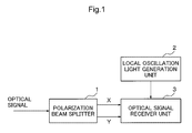
- FIG. 1 A block diagram illustrating an example of a configuration of a coherent optical receiver according to a first exemplary embodiment of the invention
- FIG. 2 A block diagram illustrating an example of a configuration of an optical signal receiver unit configuring the coherent optical receiver shown in FIG. 1
- FIG. 3 A block diagram illustrating an example of a configuration of a polarization reproduction unit configuring the optical signal receiver unit shown in FIG. 2
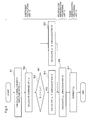
- FIG. 4 A flowchart illustrating an example of operations of the polarization reproduction unit shown in FIG. 3
- FIG. 5 A block diagram illustrating an example of a configuration of the polarization reproduction unit configuring the coherent optical receiver according to a second exemplary embodiment of the invention
- FIG. 6 A flowchart illustrating an example of operations of the polarization reproduction unit shown in FIG. 5 .
- FIG. 7 A block diagram illustrating an example of a configuration of a coherent optical receiver according to a third exemplary embodiment of the invention
- FIG. 1 is a block diagram illustrating an example of a configuration of a coherent optical receiver according to a first exemplary embodiment of the invention.
- the coherent optical receiver includes a polarization beam splitter 1 , a local oscillation light generation unit 2 , and an optical receiver unit 3 .
- the polarization beam splitter 1 separates a multi-level modulation optical signal (or referred to as single polarization multi-level phase optical signal) into an optical signal X (first optical signal) and an optical signal Y (second optical signal) whose polarization are mutually orthogonal.
- the local oscillation light generation unit 2 is, for example, a distributed-feedback laser diode, and outputs a continuous light (hereinafter referred to as local oscillation light).
- the optical receiver unit 3 performs coherent detection (e.g. homodyne detection or heterodyne detection) of the signals X and Y, and converts the detected signals into baseband signals X and Y, using the local oscillation light generated by the local oscillation light generation unit 2 . Further, the optical receiver unit 3 reproduces the transmitted multi-level modulation optical signal based on the baseband signals X and Y, and performs demodulation processing.
- coherent detection e.g. homodyne detection or heterodyne detection
- FIG. 2 is a block diagram illustrating an example of a configuration of an optical signal receiver unit 3 .
- the optical signal receiver unit 3 includes 90-degree hybrids 4 and 5 , optical/electrical conversion units 6 , 7 , 8 and 9 , a polarization reproduction unit 10 , and a demodulation processing unit 11 .
- the 90-degree hybrid 4 receives the optical signal X and the local oscillation light, and outputs optical signals each corresponding to an in-phase component and an orthogonal component.
- the optical/electrical conversion unit 6 receives an optical signal corresponding to the in-phase component of the optical signal X and outputs an in-phase baseband signal X I .
- the optical/electrical conversion unit 7 receives an optical signal corresponding to the orthogonal component of the optical signal X and outputs an orthogonal baseband signal X Q .
- the 90-degree hybrid 5 receives the optical signal Y and the local oscillation light, and outputs optical signals each corresponding to the in-phase component and the orthogonal component.
- the optical/electrical conversion unit 8 receives an optical signal corresponding to the in-phase component of the optical signal Y and outputs an in-phase baseband signal Y I .
- the optical/electrical conversion unit 9 receives an optical signal corresponding to the orthogonal component of the optical signal Y and outputs an orthogonal baseband signal Y Q .
- the polarization reproduction unit 10 receives the baseband signals X I , X Q , Y I , and Y Q from the optical/electrical conversion units 6 , 7 , 8 and 9 , respectively.
- the polarization reproduction unit 10 calculates a ratio of power ⁇ and a phase difference ⁇ between the optical signal X and the optical signal Y separated by the polarization beam splitter 1 of FIG. 1 , based on signal components included therein.
- the phase difference means a difference between phases of two waves (optical signal Y and the optical signal X).
- the polarization reproduction unit 10 reproduces an in-phase baseband signal E I and an orthogonal baseband signal E Q corresponding to transmission information based on the calculated the ratio of the power ⁇ and the phase difference ⁇ .
- the demodulation processing unit 11 demodulates the in-phase baseband signal E I and the orthogonal baseband signal E Q and extracts the transmission information.
- FIG. 3 is a block diagram illustrating an example of a configuration of the polarization reproduction unit 10 .
- the polarization reproduction unit 10 includes a coefficient calculation unit 12 , a polarization reproduction processing unit 13 and a phase reproduction processing unit 14 .
- the coefficient calculation unit 12 calculates the ratio of the power ⁇ and the phase difference ⁇ between the optical signal X and the optical signal Y based on the baseband signals X I , X Q , Y I , and Y Q .
- the polarization reproduction processing unit 13 calculates an in-phase baseband signal E I ′ and an orthogonal baseband signal E Q ′ based on the calculated ratio of the power ⁇ and the calculated phase difference ⁇ .
- the phase reproduction processing unit 14 outputs the in-phase baseband signal E I and the orthogonal baseband signal E Q in which phase offset caused by a difference between central frequencies of a signal light and a local light and/or a difference of a line width are compensated
- FIG. 4 is a flowchart illustrating an example of operations of the polarization reproduction unit 10 shown in FIG. 3 .
- FIG. 4 is explained below optionally referring to FIG. 1 to FIG. 3 .
- the coefficient calculation unit 12 calculates averages of each of the complex amplitude ratios r and ir (step S 2 ).
- the average an addition average, or a multiplication average is exemplified.
- the coefficient calculation unit 12 compares a magnitude of
- 2 +1) and ⁇ arg(r).
- 2 +1) and ⁇ ⁇ arg (ir).
- the polarization reproduction processing unit 13 outputs a real part and an imaginary part of the complex signal E s ′, as the in-phase baseband signal E I ′ and the orthogonal baseband signal E Q ′, respectively.
- the phase reproduction processing unit 14 corrects the outputted baseband signal E s ′ rotated by ⁇ (1 ⁇ ) ⁇ compared with an optical transmission signal, based on a carrier phase estimation method, e.g. Feed Forward M-th Power Algorithm, or Decision-Directed Phase-Locked Loop (step S 7 ).
- a carrier phase estimation method e.g. Feed Forward M-th Power Algorithm, or Decision-Directed Phase-Locked Loop
- the second term in the phase difference correction terms (e ⁇ j(1 ⁇ ) ⁇ , e j ⁇ ) becomes dominant compared with the first term therein.
- the ratio of the power ⁇ approaches zero, the first term in the phase difference correction terms becomes dominant compared with the second term therein.
- the multi-level phase optical signal when the multi-level phase optical signal is received, reception of the optical signal in which the receiving sensitivity does not depend on the polarization state is possible. Further, polarization reproduction can be conducted in a digital region having a low price and high reliability.
- step S 2 in FIG. 4 is not necessarily required.
- the ratio of the power ⁇ , and further the phase difference ⁇ may be averaged (addition average or multiplication average).
- the polarization reproduction processing unit 13 shown in FIG. 3 outputs a signal rotated by ⁇ (1 ⁇ ) ⁇ compared with the optical transmission signal (i.e. signal in which a phase of the combined signal is compensated on the basis of the amount of compensation after modification).
- the phase reproduction processing unit 14 shown in FIG. 4 conducts frequency compensation processing and phase compensation processing. In the above processing, a symbol may be falsely recognized. This exemplary embodiment solves the problem.
- a coherent optical receiver of the second exemplary embodiment of the invention is described below.
- a basic configuration of the coherent optical receiver is the same as the basic configuration of the first exemplary embodiment shown in FIG. 1 .
- a configuration of an optical signal receiver unit composing the coherent optical receiver is the same as that of the optical signal receiver unit 3 of the first exemplary embodiment shown in FIG. 2 . Descriptions thereof are therefore omitted.
- the second exemplary embodiment differs from the first exemplary embodiment in the configuration of the polarization reproduction unit constructing the optical signal receiver unit.
- FIG. 5 is a block diagram illustrating an example of a configuration of the polarization reproduction unit composing the coherent optical receiver according to the second exemplary embodiment of the invention.
- a polarization reproduction unit shown in FIG. 5 further includes a phase determination unit 15 and a phase rotation unit 16 .
- the phase determination unit 15 determines whether or not the phase difference ⁇ is random. The phase determination unit 15 determines whether or not to compensate the phase of the combined signal on the basis of the amount of compensation after modification, based on the ratio of the power ⁇ or the phase difference ⁇ received from the coefficient calculation unit 12 , and outputs the determination result to the phase rotation unit 16 .
- the phase rotation unit 16 based on the determination result, carries out processing which rotates, by (1 ⁇ ) ⁇ , the baseband signal E s ′ rotated by ⁇ (1 ⁇ ) ⁇ compared with the optical transmission signal and outputted, or carries out processing which outputs the baseband signal E s ′ rotated by ⁇ (1 ⁇ ) ⁇ compared with the optical transmission signal and outputted, without any change.
- FIG. 6 is a flowchart illustrating an example of operations of the polarization reproduction unit shown in FIG. 5 .
- the phase determination unit 15 receives the ratio of the power ⁇ or the phase difference ⁇ from the coefficient calculation unit 12 (step S 10 ). The phase determination unit 15 determines whether or not the phase difference ⁇ is random (step S 11 ). The phase determination unit 15 outputs the determination result to the phase rotation unit 16 .
- the phase rotation unit 16 determines whether or not the received determination result represents that the phase difference ⁇ is random (step S 12 ). If the phase difference ⁇ is random (No in step S 12 ), the phase rotation unit 16 outputs, without any change, E s ′ which is the output of the polarization reproduction processing unit 13 (i.e. signal rotated by ⁇ (1 ⁇ ) ⁇ ) to the next unit (phase reproduction processing unit 14 ). On the other hand, if the phase difference ⁇ is not random (Yes in step S 12 ), the phase rotation unit 16 rotates E s ′ which is the output of the polarization reproduction processing unit 13 by (1 ⁇ ) ⁇ and outputs the rotated signal (step S 14 ).
- the phase rotation unit 16 rotates E s ′ which is the output of the polarization reproduction processing unit 13 by (1 ⁇ ) ⁇ and outputs the rotated signal. It is therefore avoidable to falsely recognize a symbol in the phase reproduction processing unit 14 .
- the phase determination unit 15 determines that the phase difference ⁇ is not random.
- which is the difference between the phase difference ⁇ [t] at a sampling time and the phase difference ⁇ [t+1] at the next sampling time with respect to each sampling time. If the number of times in which the value exceeds the threshold value Dth 0.5 is k, it is determined that the phase difference ⁇ is random, when k reaches 3.
- the threshold value and the number of times k in which the threshold value is exceeded can be arbitrarily set.
- the phase difference determination may be consecutively performed and periodically performed in accordance with a time schedule.
- the phase determination unit 15 can perform the above determination using the ratio of the power ⁇ . For example the phase determination unit 15 can determine the phase difference ⁇ is random if ⁇ 1, 0, and the phase difference ⁇ is not random if 0 ⁇ 1.
- phase determination unit 15 is not limited thereto.
- FIG. 7 is a block diagram illustrating an example of a configuration of an optical receiver 100 according to a third exemplary embodiment of the invention.
- the optical receiver 100 includes a separation means 101 , calculation means 102 , and combination means 103 .
- the separation means 101 separates a single polarization multi-level phase optical signal into a first optical signal and a second optical signal which are mutually orthogonal.
- the calculation means 102 calculates a ratio of power of the first optical signal to power of the second optical signal, and a difference between a phase of the first optical signal and a phase of the second optical signal, as an amount of compensation.
- the combination means 103 combines, based on the ratio and the amount of compensation, the first optical signal and the second optical signal using a maximal ratio combining method.
- the combination means 103 modifies the amount of compensation based on the ratio.
- reception in which receiving sensitivity does not depend on a polarization state can be performed.
- the first to the third exemplary embodiments above described may be materialized as given hardware, e.g. a circuit.
- the first to the third exemplary embodiments above described may be controlled and operated by a computer circuit (e.g. CPU (Central Processing Unit), not shown) based on a control program.
- the control program is stored in, for example, a storage medium in an optical receiver or an external storage medium, and is read and executed by the computer circuit.
- a ROM (Read Only Memory) or a hard disc is exemplified as an internal storage medium.
- a removable media or a removable disc is exemplified as the external storage medium.
- the first to the third exemplary embodiments above described are examples, and the invention is not limited to the exemplary embodiments above described.
Landscapes
- Physics & Mathematics (AREA)
- Electromagnetism (AREA)
- Engineering & Computer Science (AREA)
- Computer Networks & Wireless Communication (AREA)
- Signal Processing (AREA)
- Optical Communication System (AREA)
Applications Claiming Priority (3)
| Application Number | Priority Date | Filing Date | Title |
|---|---|---|---|
| JP2011095190 | 2011-04-21 | ||
| JP2011-095190 | 2011-04-21 | ||
| PCT/JP2011/079115 WO2012144108A1 (fr) | 2011-04-21 | 2011-12-09 | Procédé de réception optique et récepteur optique |
Publications (2)
| Publication Number | Publication Date |
|---|---|
| US20140044440A1 US20140044440A1 (en) | 2014-02-13 |
| US9154232B2 true US9154232B2 (en) | 2015-10-06 |
Family
ID=47041245
Family Applications (1)
| Application Number | Title | Priority Date | Filing Date |
|---|---|---|---|
| US14/112,653 Active 2032-01-02 US9154232B2 (en) | 2011-04-21 | 2011-12-09 | Optical reception method and optical receiver using maximal-ratio-combining method |
Country Status (3)
| Country | Link |
|---|---|
| US (1) | US9154232B2 (fr) |
| JP (1) | JPWO2012144108A1 (fr) |
| WO (1) | WO2012144108A1 (fr) |
Families Citing this family (5)
| Publication number | Priority date | Publication date | Assignee | Title |
|---|---|---|---|---|
| US8886058B2 (en) * | 2012-06-04 | 2014-11-11 | Cisco Technology, Inc. | Cycle slip reduction in coherent optical communications |
| CN104303435B (zh) * | 2013-03-18 | 2016-10-12 | 华为技术有限公司 | 相干光通信的装置和方法 |
| US9967028B2 (en) | 2014-10-22 | 2018-05-08 | Indian Institute Of Technology Delhi | System and a method for free space optical communications |
| US9680574B1 (en) * | 2015-11-30 | 2017-06-13 | Futurewei Technologies, Inc. | Frequency domain optical channel estimation |
| CN113132014B (zh) * | 2019-12-31 | 2022-07-01 | 烽火通信科技股份有限公司 | 一种光互连通信方法及系统 |
Citations (21)
| Publication number | Priority date | Publication date | Assignee | Title |
|---|---|---|---|---|
| US4965858A (en) * | 1988-02-19 | 1990-10-23 | Fujitsu Limited | Polarization diversity optical receiver for coherent optical communication |
| US5003626A (en) * | 1986-06-20 | 1991-03-26 | Fujitsu Limited | Dual balanced optical signal receiver |
| US5142402A (en) * | 1988-12-16 | 1992-08-25 | Hitachi, Ltd. | Polarization diversity optical receiving apparatus and method |
| JPH05224267A (ja) | 1992-02-10 | 1993-09-03 | Toshiba Corp | 光受信器 |
| US5253097A (en) * | 1990-07-18 | 1993-10-12 | Fujitsu Limited | Demodulator and a polarization diversity receiver for coherent optical communication provided with the demodulator |
| US5388088A (en) * | 1992-04-02 | 1995-02-07 | At&T Corp. | Multiple polarization sensitive detection arrangement for fiber optic communications |
| US5523875A (en) * | 1995-04-24 | 1996-06-04 | Scientific-Atlanta, Inc. | Automatic gain control circuit |
| JP2001333005A (ja) | 2000-05-24 | 2001-11-30 | Ntt Docomo Inc | 光空間伝送システム、光空間伝送方法及び光空間伝送装置 |
| US20020109885A1 (en) * | 2001-02-15 | 2002-08-15 | Ntt Docomo, Inc. | Information transmission system and information transmission method, and, optical space transmission system and optical space transmission method |
| US20080159758A1 (en) * | 2003-09-22 | 2008-07-03 | Celight, Inc. | Optical orthogonal frequency division multiplexed communications with coherent detection |
| US20090208224A1 (en) * | 2006-05-11 | 2009-08-20 | Hitachi Communication Technologies, Ltd. | Optical field receiver, optical multilevel signal receiver, and optical transmission system |
| JP2010212886A (ja) | 2009-03-09 | 2010-09-24 | Nec Corp | 光受信装置、光送信装置、通信システム、光信号多重方法、光信号分離方法及びプログラム |
| US20100254718A1 (en) * | 2009-04-03 | 2010-10-07 | Fujitsu Limited | Optical receiver and method for optical reception |
| JP2011009956A (ja) | 2009-06-24 | 2011-01-13 | Fujitsu Ltd | デジタルコヒーレント受信器 |
| US20110182589A1 (en) * | 2010-01-28 | 2011-07-28 | Hitachi, Ltd. | Optical Transmission and Reception System, and Optical Receiver |
| WO2011099589A1 (fr) | 2010-02-09 | 2011-08-18 | 日本電気株式会社 | Dispositif de compensation d'excursion de phase/d'excursion de fréquence d'onde de porteuse et procédé de compensation d'excursion de phase/d'excursion de fréquence d'onde de porteuse |
| US20110305457A1 (en) * | 2009-03-02 | 2011-12-15 | Hitachi, Ltd. | Optical Multi-Level Transmission System |
| US20120134676A1 (en) * | 2010-11-29 | 2012-05-31 | Hitachi, Ltd. | Polarization-Multiplexed Optical Transmission System, Polarization-Multiplexed Optical Transmitter, and Polarization-Multiplexed Optical Receiver |
| US20120183303A1 (en) * | 2009-09-29 | 2012-07-19 | Mitsubishi Electric Corporation | Multilevel modulated optical transceiver and multilevel modulated optical transmitting/receiving method |
| US20120315043A1 (en) * | 2010-02-04 | 2012-12-13 | Nippon Telegraph And Telephone Corporation | Transmission method, reception method, transmitter apparatus, and receiver device |
| US20130216228A1 (en) * | 2010-06-22 | 2013-08-22 | Moshe Nazarathy | Optical network unit, optical access network and a method for exchanging information |
-
2011
- 2011-12-09 WO PCT/JP2011/079115 patent/WO2012144108A1/fr not_active Ceased
- 2011-12-09 US US14/112,653 patent/US9154232B2/en active Active
- 2011-12-09 JP JP2013510847A patent/JPWO2012144108A1/ja active Pending
Patent Citations (22)
| Publication number | Priority date | Publication date | Assignee | Title |
|---|---|---|---|---|
| US5003626A (en) * | 1986-06-20 | 1991-03-26 | Fujitsu Limited | Dual balanced optical signal receiver |
| US4965858A (en) * | 1988-02-19 | 1990-10-23 | Fujitsu Limited | Polarization diversity optical receiver for coherent optical communication |
| US5142402A (en) * | 1988-12-16 | 1992-08-25 | Hitachi, Ltd. | Polarization diversity optical receiving apparatus and method |
| US5253097A (en) * | 1990-07-18 | 1993-10-12 | Fujitsu Limited | Demodulator and a polarization diversity receiver for coherent optical communication provided with the demodulator |
| JPH05224267A (ja) | 1992-02-10 | 1993-09-03 | Toshiba Corp | 光受信器 |
| US5388088A (en) * | 1992-04-02 | 1995-02-07 | At&T Corp. | Multiple polarization sensitive detection arrangement for fiber optic communications |
| US5523875A (en) * | 1995-04-24 | 1996-06-04 | Scientific-Atlanta, Inc. | Automatic gain control circuit |
| JP2001333005A (ja) | 2000-05-24 | 2001-11-30 | Ntt Docomo Inc | 光空間伝送システム、光空間伝送方法及び光空間伝送装置 |
| US20020109885A1 (en) * | 2001-02-15 | 2002-08-15 | Ntt Docomo, Inc. | Information transmission system and information transmission method, and, optical space transmission system and optical space transmission method |
| US20080159758A1 (en) * | 2003-09-22 | 2008-07-03 | Celight, Inc. | Optical orthogonal frequency division multiplexed communications with coherent detection |
| US20090208224A1 (en) * | 2006-05-11 | 2009-08-20 | Hitachi Communication Technologies, Ltd. | Optical field receiver, optical multilevel signal receiver, and optical transmission system |
| US20110305457A1 (en) * | 2009-03-02 | 2011-12-15 | Hitachi, Ltd. | Optical Multi-Level Transmission System |
| JP2010212886A (ja) | 2009-03-09 | 2010-09-24 | Nec Corp | 光受信装置、光送信装置、通信システム、光信号多重方法、光信号分離方法及びプログラム |
| US20100254718A1 (en) * | 2009-04-03 | 2010-10-07 | Fujitsu Limited | Optical receiver and method for optical reception |
| JP2011009956A (ja) | 2009-06-24 | 2011-01-13 | Fujitsu Ltd | デジタルコヒーレント受信器 |
| US20120183303A1 (en) * | 2009-09-29 | 2012-07-19 | Mitsubishi Electric Corporation | Multilevel modulated optical transceiver and multilevel modulated optical transmitting/receiving method |
| US20110182589A1 (en) * | 2010-01-28 | 2011-07-28 | Hitachi, Ltd. | Optical Transmission and Reception System, and Optical Receiver |
| US20120315043A1 (en) * | 2010-02-04 | 2012-12-13 | Nippon Telegraph And Telephone Corporation | Transmission method, reception method, transmitter apparatus, and receiver device |
| WO2011099589A1 (fr) | 2010-02-09 | 2011-08-18 | 日本電気株式会社 | Dispositif de compensation d'excursion de phase/d'excursion de fréquence d'onde de porteuse et procédé de compensation d'excursion de phase/d'excursion de fréquence d'onde de porteuse |
| US20120299629A1 (en) * | 2010-02-09 | 2012-11-29 | Nec Corporation | Phase excursion/carrier wave frequency excursion compensation device and phase excursion/carrier wave frequency excursion compensation method |
| US20130216228A1 (en) * | 2010-06-22 | 2013-08-22 | Moshe Nazarathy | Optical network unit, optical access network and a method for exchanging information |
| US20120134676A1 (en) * | 2010-11-29 | 2012-05-31 | Hitachi, Ltd. | Polarization-Multiplexed Optical Transmission System, Polarization-Multiplexed Optical Transmitter, and Polarization-Multiplexed Optical Receiver |
Non-Patent Citations (6)
| Title |
|---|
| International Search Report for PCT Application No. PCT/JP2011/079115, Mailed on Mar. 6, 2012. |
| Japanese Office Action for JP Application No. 2013-510847 mailed on Jul. 21, 2015 with English Translation. |
| K. Kikuchi and S. Tsukamoto, Evaluation of Sensitivity of the Digital Coherent Receiver, Journal of Lightwave Technology, vol. 26, No. 13, pp. 1817-1822 (Jul. 2008) Cited in JPOA. |
| Kikuchi et al, Evaluation of Sensitivity of the Digital Coherent Receiver, Jul. 2008, JLT vol. 26 issue 13, pp. 1817-1822. * |
| Kikuchi, K., "Optical Homodyne Receiver Comprising Phase and Polarization Diversities with Digital Signal Processing," IEEE/LEOS Summer Topical Meetings, 2007 Digest of the , vol., No., pp. 55,56, Jul. 23-25, 2007. * |
| Satoshi Tsukamoto et al., "Optical Homodyne Receiver Comprising Phase and Polarization Diversities with Digital Signal Processing". (From IEEE Xplore, Downloaded on Jul. 14, 2010). |
Also Published As
| Publication number | Publication date |
|---|---|
| US20140044440A1 (en) | 2014-02-13 |
| WO2012144108A1 (fr) | 2012-10-26 |
| JPWO2012144108A1 (ja) | 2014-07-28 |
Similar Documents
| Publication | Publication Date | Title |
|---|---|---|
| US8406635B2 (en) | Optical communication system and optical receiver | |
| US9048957B2 (en) | Signal processing circuit, optical receiver, detector and method for compensating for waveform distortion | |
| US10439732B2 (en) | Receiving device and phase-error compensation method | |
| US8478137B2 (en) | Optical receiver | |
| US9112614B2 (en) | Correction of a local-oscillator phase error in a coherent optical receiver | |
| US20120082464A1 (en) | Coherent optical receiving apparatus, coherent optical communications system employing same, and coherent optical communications method | |
| US9154232B2 (en) | Optical reception method and optical receiver using maximal-ratio-combining method | |
| US9401765B2 (en) | Frequency offset estimation circuit and frequency offset estimation method | |
| US8660438B2 (en) | Digital coherent receiver and receiving method | |
| JP2012070051A (ja) | コヒーレント光受信器およびその制御方法 | |
| US9020337B2 (en) | Receiver and failure detection method for receiver | |
| US20120148266A1 (en) | Digital coherent optical receiver, adaptive equalizer, and digital coherent optical communication method | |
| CN101273567B (zh) | 交叉极化干扰消除方法和交叉极化干扰消除设备 | |
| US20140212149A1 (en) | Soft decoding of data in a coherent optical receiver | |
| EP2169867B1 (fr) | Algorithme axé sur la décision pour le réglage d'un démultiplexeur de polarisation dans un récepteur optique cohérent de détection | |
| US11139896B2 (en) | Signal processing device and signal processing method | |
| US20140286638A1 (en) | Signal processing apparatus and signal processing method | |
| US9515743B2 (en) | Receiver, transmission system, method for receiving polarization multiplexed optical signal, and non-transitory computer readable medium storing receiver control program | |
| US11476946B2 (en) | Signal processing device and transmission device | |
| US9306675B2 (en) | Digital coherent receiver, optical reception system, and optical reception method | |
| JP2018078544A (ja) | バイアスドリフト補償装置、受信信号復元装置及び受信機 | |
| JP2014154926A (ja) | 受信信号処理装置および受信信号処理方法 | |
| JP5685908B2 (ja) | ループフィルタ | |
| JP2017175326A (ja) | デジタルコヒーレント受信装置、光空間通信システム及びそのドップラーシフト捕捉方法 | |
| JP2022060607A (ja) | 光送信機および光送信機の制御方法 |
Legal Events
| Date | Code | Title | Description |
|---|---|---|---|
| AS | Assignment |
Owner name: NEC CORPORATION, JAPAN Free format text: ASSIGNMENT OF ASSIGNORS INTEREST;ASSIGNORS:ENDO, KAZUOMI;HASHIMOTO, YOICHI;REEL/FRAME:031433/0781 Effective date: 20130920 |
|
| STCF | Information on status: patent grant |
Free format text: PATENTED CASE |
|
| MAFP | Maintenance fee payment |
Free format text: PAYMENT OF MAINTENANCE FEE, 4TH YEAR, LARGE ENTITY (ORIGINAL EVENT CODE: M1551); ENTITY STATUS OF PATENT OWNER: LARGE ENTITY Year of fee payment: 4 |
|
| MAFP | Maintenance fee payment |
Free format text: PAYMENT OF MAINTENANCE FEE, 8TH YEAR, LARGE ENTITY (ORIGINAL EVENT CODE: M1552); ENTITY STATUS OF PATENT OWNER: LARGE ENTITY Year of fee payment: 8 |