US9250210B2 - Gas sensor - Google Patents
Gas sensor Download PDFInfo
- Publication number
- US9250210B2 US9250210B2 US14/366,912 US201214366912A US9250210B2 US 9250210 B2 US9250210 B2 US 9250210B2 US 201214366912 A US201214366912 A US 201214366912A US 9250210 B2 US9250210 B2 US 9250210B2
- Authority
- US
- United States
- Prior art keywords
- gas
- carbon nanotube
- ionic liquid
- gas sensor
- source
- Prior art date
- Legal status (The legal status is an assumption and is not a legal conclusion. Google has not performed a legal analysis and makes no representation as to the accuracy of the status listed.)
- Expired - Fee Related, expires
Links
Images


Classifications
-
- G—PHYSICS
- G01—MEASURING; TESTING
- G01N—INVESTIGATING OR ANALYSING MATERIALS BY DETERMINING THEIR CHEMICAL OR PHYSICAL PROPERTIES
- G01N27/00—Investigating or analysing materials by the use of electric, electrochemical, or magnetic means
-
- G—PHYSICS
- G01—MEASURING; TESTING
- G01N—INVESTIGATING OR ANALYSING MATERIALS BY DETERMINING THEIR CHEMICAL OR PHYSICAL PROPERTIES
- G01N27/00—Investigating or analysing materials by the use of electric, electrochemical, or magnetic means
- G01N27/26—Investigating or analysing materials by the use of electric, electrochemical, or magnetic means by investigating electrochemical variables; by using electrolysis or electrophoresis
- G01N27/416—Systems
- G01N27/48—Systems using polarography, i.e. measuring changes in current under a slowly-varying voltage
-
- G—PHYSICS
- G01—MEASURING; TESTING
- G01N—INVESTIGATING OR ANALYSING MATERIALS BY DETERMINING THEIR CHEMICAL OR PHYSICAL PROPERTIES
- G01N27/00—Investigating or analysing materials by the use of electric, electrochemical, or magnetic means
- G01N27/26—Investigating or analysing materials by the use of electric, electrochemical, or magnetic means by investigating electrochemical variables; by using electrolysis or electrophoresis
- G01N27/403—Cells and electrode assemblies
- G01N27/414—Ion-sensitive or chemical field-effect transistors, i.e. ISFETS or CHEMFETS
- G01N27/4141—Ion-sensitive or chemical field-effect transistors, i.e. ISFETS or CHEMFETS specially adapted for gases
-
- G—PHYSICS
- G01—MEASURING; TESTING
- G01N—INVESTIGATING OR ANALYSING MATERIALS BY DETERMINING THEIR CHEMICAL OR PHYSICAL PROPERTIES
- G01N27/00—Investigating or analysing materials by the use of electric, electrochemical, or magnetic means
- G01N27/26—Investigating or analysing materials by the use of electric, electrochemical, or magnetic means by investigating electrochemical variables; by using electrolysis or electrophoresis
- G01N27/403—Cells and electrode assemblies
- G01N27/414—Ion-sensitive or chemical field-effect transistors, i.e. ISFETS or CHEMFETS
- G01N27/4146—Ion-sensitive or chemical field-effect transistors, i.e. ISFETS or CHEMFETS involving nanosized elements, e.g. nanotubes, nanowires
-
- G—PHYSICS
- G01—MEASURING; TESTING
- G01N—INVESTIGATING OR ANALYSING MATERIALS BY DETERMINING THEIR CHEMICAL OR PHYSICAL PROPERTIES
- G01N33/00—Investigating or analysing materials by specific methods not covered by groups G01N1/00 - G01N31/00
- G01N33/0004—Gaseous mixtures, e.g. polluted air
- G01N33/0009—General constructional details of gas analysers, e.g. portable test equipment
- G01N33/0027—General constructional details of gas analysers, e.g. portable test equipment concerning the detector
- G01N33/0036—General constructional details of gas analysers, e.g. portable test equipment concerning the detector specially adapted to detect a particular component
- G01N33/004—CO or CO2
-
- G—PHYSICS
- G01—MEASURING; TESTING
- G01N—INVESTIGATING OR ANALYSING MATERIALS BY DETERMINING THEIR CHEMICAL OR PHYSICAL PROPERTIES
- G01N33/00—Investigating or analysing materials by specific methods not covered by groups G01N1/00 - G01N31/00
- G01N33/0004—Gaseous mixtures, e.g. polluted air
- G01N33/0009—General constructional details of gas analysers, e.g. portable test equipment
- G01N33/0027—General constructional details of gas analysers, e.g. portable test equipment concerning the detector
- G01N33/0036—General constructional details of gas analysers, e.g. portable test equipment concerning the detector specially adapted to detect a particular component
- G01N33/0054—Ammonia
-
- H—ELECTRICITY
- H10—SEMICONDUCTOR DEVICES; ELECTRIC SOLID-STATE DEVICES NOT OTHERWISE PROVIDED FOR
- H10D—INORGANIC ELECTRIC SEMICONDUCTOR DEVICES
- H10D30/00—Field-effect transistors [FET]
- H10D30/60—Insulated-gate field-effect transistors [IGFET]
- H10D30/67—Thin-film transistors [TFT]
-
- H—ELECTRICITY
- H10—SEMICONDUCTOR DEVICES; ELECTRIC SOLID-STATE DEVICES NOT OTHERWISE PROVIDED FOR
- H10K—ORGANIC ELECTRIC SOLID-STATE DEVICES
- H10K10/00—Organic devices specially adapted for rectifying, amplifying, oscillating or switching; Organic capacitors or resistors having potential barriers
-
- H01L51/0048—
-
- H01L51/0508—
-
- H—ELECTRICITY
- H10—SEMICONDUCTOR DEVICES; ELECTRIC SOLID-STATE DEVICES NOT OTHERWISE PROVIDED FOR
- H10K—ORGANIC ELECTRIC SOLID-STATE DEVICES
- H10K10/00—Organic devices specially adapted for rectifying, amplifying, oscillating or switching; Organic capacitors or resistors having potential barriers
- H10K10/40—Organic transistors
- H10K10/46—Field-effect transistors, e.g. organic thin-film transistors [OTFT]
-
- H—ELECTRICITY
- H10—SEMICONDUCTOR DEVICES; ELECTRIC SOLID-STATE DEVICES NOT OTHERWISE PROVIDED FOR
- H10K—ORGANIC ELECTRIC SOLID-STATE DEVICES
- H10K85/00—Organic materials used in the body or electrodes of devices covered by this subclass
- H10K85/20—Carbon compounds, e.g. carbon nanotubes or fullerenes
- H10K85/221—Carbon nanotubes
-
- Y—GENERAL TAGGING OF NEW TECHNOLOGICAL DEVELOPMENTS; GENERAL TAGGING OF CROSS-SECTIONAL TECHNOLOGIES SPANNING OVER SEVERAL SECTIONS OF THE IPC; TECHNICAL SUBJECTS COVERED BY FORMER USPC CROSS-REFERENCE ART COLLECTIONS [XRACs] AND DIGESTS
- Y02—TECHNOLOGIES OR APPLICATIONS FOR MITIGATION OR ADAPTATION AGAINST CLIMATE CHANGE
- Y02A—TECHNOLOGIES FOR ADAPTATION TO CLIMATE CHANGE
- Y02A50/00—TECHNOLOGIES FOR ADAPTATION TO CLIMATE CHANGE in human health protection, e.g. against extreme weather
- Y02A50/20—Air quality improvement or preservation, e.g. vehicle emission control or emission reduction by using catalytic converters
Definitions
- the present invention relates to a gas sensor, and is suitable to be applied to detection of, for example, gases such as CO 2 and NH 3 .
- the gas sensor using a carbon nanotube like this has a configuration in which the surfaces of the carbon nanotube provided between a source electrode and a drain electrode are chemically modified with two kinds of polymers, in order to detect CO 2 that is a target of detection, for example.
- the gas sensor is configured in such a manner that the carbon nanotube is disposed on the silicon back gate via a silicon oxide film, and a gate voltage can be applied to the silicon back gate.
- An object of the present invention is to propose a gas sensor capable of enhancing gas detection sensitivity more than the conventional gas sensors, with a simple configuration.
- a first aspect of the present invention is a gas sensor that detects a gas that is a target of detection
- the gas sensor includes: a carbon nanotube provided between a source electrode and a drain electrode on a substrate, and a source-drain current flows therein; and a gas absorbing liquid disposed to cover the carbon nanotube, and is featured in that the gas is detected based on a change of the source-drain current in the carbon nanotube caused by absorbing the gas in the gas absorbing liquid.
- a second aspect of the present invention is the gas sensor, wherein the gas absorbing liquid is in contact with the carbon nanotube and a gate electrode on the substrate to become a gate insulating layer, a state of the gate insulating layer changes by absorbing the gas, and the gas is detected based on a change of the source-drain current that occurs in response to the state of the gate insulating layer.
- the change of the state of the electric charges in the gas absorbing liquid, which occurs by absorption of a gas is directly reflected in the source-drain current that flows in the carbon nanotube, and therefore, gas detection sensitivity can be enhanced more than the conventional gas sensors. Further, since surface chemical modification does not have to be performed for the carbon nanotube itself as in the conventional gas sensors, and the gas absorbing liquid only has to be provided so as to be in contact with the carbon nanotube, the configuration can be simplified correspondingly.
- the change of the state of the gate insulating layer of the gas absorbing liquid, which occurs by absorption of the gas is directly reflected in the source-drain current that flows in the carbon nanotube, and therefore, gas detection sensitivity can be enhanced more than in the conventional gas sensors.
- the configuration can be simplified correspondingly.
- FIG. 1 is a perspective view showing a configuration of a gas sensor according to the present invention
- FIG. 2 is a schematic view showing a top surface configuration of the gas sensor according to the present invention.
- FIG. 3 is a sectional view showing a sectional configuration of an A-A′ portion in FIG. 2 ;
- FIG. 4 is a sectional view showing a sectional configuration of a B-B′ portion in FIG. 2 ;
- FIG. 5 is a schematic view presented for explanation of an electric double layer
- FIG. 6 is a graph showing change of a source-drain current and a gate voltage
- FIG. 7 is a schematic view presented for explanation (1) of a method of producing the gas sensor
- FIG. 8 is a schematic view presented for explanation (2) of the method of producing the gas sensor
- FIG. 9 is a schematic view presented for explanation (3) of the method of producing the gas sensor.
- FIG. 10 is a schematic view presented for explanation (4) of the method of producing the gas sensor
- FIG. 11 is a schematic view presented for explanation (5) of the method of producing the gas sensor
- FIG. 12 is a photograph showing a configuration of the gas sensor actually produced
- FIG. 13 is a photograph of a part of FIG. 12 that is enlarged, and an SEM photograph showing a detailed configuration of a carbon nanotube;
- FIG. 14 is a graph showing a relation of a source-drain current I sd and a gate voltage V g , obtained by the gas sensor;
- FIG. 15 is a graph showing a relation of a leak current I g and the gate voltage V g ;
- FIG. 16 is a schematic view showing an entire configuration of an experimental apparatus
- FIG. 17 is a graph showing relation of the source-drain current I sd and the gate voltage V g in the case of a mixture gas of CO 2 and outside air, and in the case of only outside air;
- FIG. 18 is a graph showing relation of the source-drain current I sd and the gate voltage V g in the case of a mixture gas of NH 3 and outside air, and in the case of only outside air;
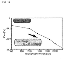
- FIG. 19 is a graph showing a relation of a shift voltage V shift and an NH 3 concentration
- FIG. 20 is a graph showing relation of the source-drain current I sd and the gate voltage V g by the gas sensor using a metallic carbon nanotube;
- FIG. 21 is a graph showing relation of the source-drain current I sd and the gate voltage V g by the gas sensor using a semiconductor carbon nanotube;
- FIG. 22 is a perspective view showing a configuration of a gas sensor ( 1 ) according to another embodiment
- FIG. 23 is a sectional view showing a sectional configuration of a C-C′ portion in FIG. 22 ;
- FIG. 24 is a sectional view showing a sectional configuration of a D-D′ portion in FIG. 22 ;
- FIG. 25 is a sectional view showing a sectional configuration of a gas sensor ( 2 ) according to another embodiment.
- FIG. 26 is a perspective view showing a configuration of a gas sensor ( 3 ) according to another embodiment.
- a gas sensor according to the present invention is denoted by 1
- the gas sensor 1 is configured so as to be able to detect a gas, for example, such as CO 2 and NH 3 , as a target of detection.
- the gas sensor 1 includes a source electrode 3 and a drain electrode 4 in band shapes on a substrate 2 formed into a plate shape, and a carbon nanotube 8 is provided between the source electrode 3 and the drain electrode 4 .
- the source electrode 3 and the drain electrode 4 are formed from, for example, a Ti/Au material or a Cr/Au material, and disposed substantially rectilinearly with respective longitudinal directions being aligned with each other, so that a gap of approximately 1 ⁇ m is formed between an end portion of the source electrode 3 and an end portion of the drain electrode 4 that face each other.
- the carbon nanotube 8 has one end side electrically connected to the end portion of the source electrode 3 and the other end side electrically connected to the end portion of the drain electrode 4 , and is disposed so as to be positioned to form a straight line with the source electrode 3 and the drain electrode 4 .
- the carbon nanotube 8 has a configuration in which a six-membered ring structure is rolled into a cylindrical shape in carbon, and has a large specific surface area, the carbon nanotube 8 correspondingly has a large contact surface to be in contact with an ionic liquid IL that will be described later, and also include excellent conductivity.
- the substrate 2 is provided with a gate electrode 7 formed from, for example, a Ti/Au material and a Cu/Au material, the ionic liquid IL is placed so as to be in contact with the gate electrode 7 , and the carbon nanotube 8 is configured to be able to be contained in the ionic liquid IL.
- the gate electrode 7 is formed by a first gate electrode portion 5 and a second gate electrode portion 6 that are formed into the same shape and size, and the carbon nanotube 8 , the source electrode 3 and the drain electrode 4 can be disposed in a gap G 1 between the first gate electrode portion 5 and the second gate electrode portion 6 . More specifically, in the case of this embodiment, as in FIG. 2 showing a top surface configuration of an area E of FIG.
- the first gate electrode portion 5 and the second gate electrode portion 6 are formed into semi-circular shapes, a straight line portion 5 a of the first gate electrode portion 5 and a straight line portion 6 a of the second gate electrode portion 6 are disposed in parallel with each other with the predetermined gap G 1 therebetween.
- the carbon nanotube 8 , the source electrode 3 and the drain electrode 4 are disposed rectilinearly with respective longitudinal directions being aligned with one another.
- the ionic liquid IL is placed in a semi-spherical shape over the first gate electrode portion 5 , the second gate electrode portion 6 , the source electrode 3 and the drain electrode 4 in such a manner as to cover the entire carbon nanotube 8 , and is configured to be able to function as a gate insulating layer.
- the ionic liquid IL is configured so that a semi-spherical liquid surface is exposed to outside air, and can contain the carbon nanotube 8 that is located in a central portion of the first gate electrode portion 5 , the second gate electrode portion 6 , the source electrode 3 and the drain electrode 4 .
- the ionic liquid IL as a gas absorbing liquid is formed from, for example, [EMIM][BF 4 ](1-ethyl-3-methylimidazolium Tetrafluoroborate), [BMIM][BF 4 ](1-Butyl-3-methylimidazolium Tetrafluoroborate), [BMIM][PF 6 ](1-Butyl-3-methylimidazolium Hexafluorophosphate), or [OMIM][Br](1-n-octyl-3-methylimidazolium bromide), besides the above, [Hmpy][Tf 2 N], [HMIM][Tf 2 N], [BMIM][Tf 2 N], [C 6 H 4 F 9 min][Tf 2 N], [AMIM][BF 4 ], [Pabim][BF 4 ], [Am-im][DCA], [Am-im][BF 4 ], [BMIM][BF 4 ]+PVDF, [C 3 NH
- PEI polyethyleneimine
- the amino group of PEI transfers electric charges to the carbon nanotube 8 , and can reduce the resistance value of the carbon nanotube 8 .
- PEI reacts with CO 2 and H 2 O when the ionic liquid IL absorbs a gas, and the amino group of PEI decreases.
- the amino group of PEI in the ionic liquid IL decreases when the ionic liquid IL absorbs outside air with a high CO 2 content, as a result of which, the resistance value of the carbon nanotube 8 can increase, and an electric state of the carbon nanotube 8 can change in accordance with the CO 2 content in the outside air.
- the gas absorbing liquid IL is applied as the gas absorbing liquid
- various other gas absorbing liquids such as hydroxide aqueous solutions of an alkali metal and an alkaline earth metal may be applied.
- hydroxide aqueous solutions of an alkali metal and an alkaline earth metal are used as the gas absorbing liquid, the gas absorbing liquids can absorb CO 2 , and therefore, the gas sensor the detection target of which is CO 2 can be realized.
- the substrate 2 on which the ionic liquid IL is placed has a configuration in which a silicon oxide film 11 is formed on a silicon substrate 10 , and has a configuration in which the source electrode 3 , the drain electrode 4 , the first gate electrode portion 5 and the second gate electrode portion 6 are provided on the silicon oxide film 11 . Further, as shown in FIG. 3 showing a sectional configuration of an A-A′ portion in FIG. 2 , and FIG. 4 showing a sectional configuration of a B-B′ portion in FIG. 2 , the substrate 2 on which the ionic liquid IL is placed has a configuration in which a silicon oxide film 11 is formed on a silicon substrate 10 , and has a configuration in which the source electrode 3 , the drain electrode 4 , the first gate electrode portion 5 and the second gate electrode portion 6 are provided on the silicon oxide film 11 . Further, as shown in FIG.
- the carbon nanotube 8 is configured so as to have one end side covered with the source electrode 3 and the other end side covered with the drain electrode 4 , and to be capable of being electrically connected to the source electrode 3 and the drain electrode 4 . Further, the carbon nanotube 8 can have both the ends reliably fixed to the substrate 2 by having both the ends covered with the source electrode 3 and the drain electrode 4 , and therefore, can keep an electric connection state to the source electrode 3 and the drain electrode 4 as it is without being removed from the substrate 2 when the ionic liquid IL is dropped.
- the carbon nanotube 8 as above has a diameter of approximately 1 to 10 nm, and is formed by growing in a straight line shape along the silicon oxide film 11 from a catalyst portion 12 provided on the silicon oxide film 11 .
- the catalyst portion 12 is formed from a material prepared by, for example, mixing Co and silica at a predetermined ratio, and is covered with the drain electrode 4 together with the other end of the carbon nanotube 8 .
- the gas sensor 1 like this is configured so that a source-drain current is supplied to the drain electrode 4 from the source electrode 3 by a power supply 13 as shown in FIG. 3 , and as shown in FIG. 4 , a gate voltage can be applied to the first gate electrode portion 5 and the second gate electrode portion 6 by a power supply 15 .
- anions in the ionic liquid IL gather on the side peripheral surface of the carbon nanotube 8
- cations in the ionic liquid IL gather on the first gate electrode portion 5
- an electric double layer two layers that are a layer in which marks of circled “ ⁇ ” are written and a layer in which marks of circled “+” are written in FIG. 5
- the ionic liquid IL can be a gate insulating layer.
- a gate voltage V g is applied to the first gate electrode portion 5 and the second gate electrode portion 6
- a source-drain voltage V sd is applied between the source electrode 3 and the drain electrode 4 , whereby an extremely thin gate insulating layer is formed in the ionic liquid IL, a source-drain current I sd flows in the carbon nanotube 8 , and the gas sensor can operate as a transistor.
- the state of the gate insulating layer in the ionic liquid IL can be changed in accordance with the absorption amount of the gas, and source-drain current/gate voltage characteristics also can change in accordance with the change of the state of the gate insulating layer.
- the gas sensor 1 such the change of the source-drain current/gate voltage characteristics is measured, and the gas that is a target of detection can be detected based on the change of the source-drain current/gate voltage characteristics. Further, with the gas sensor 1 , the change amount of the source-drain current/gate voltage characteristics is measured, and when the change amount is large, it is indicated that a gas concentration in the gas (hereinafter, also simply called outside air) around the ionic liquid IL is high, whereas when the change amount is small, it is indicated that the gas concentration in the outside air is low, so that the gas concentration in the outside air can be estimated.
- a gas concentration in the gas hereinafter, also simply called outside air
- a waveform close to a substantially V-shape can be obtained as the relationship between the source drain current I sd and the gate voltage V g when the gas that is a target of detection is not contained in the gas around the ionic liquid IL, as shown in FIG. 6 .
- the gate voltage V g in the gas sensor 1 can shift by a shift voltage V shift .
- the shift voltage V shift can increase in proportion thereto.
- the gas sensor 1 of the present invention detection of the gas contained in outside air and estimation of the content of the gas are enabled based on a change of the source-drain current I sd , and the change of the gate voltage V g that occurs due to the change of the source-drain current I sd .
- the gas sensor 1 which is provided with the gate electrode 7 , applies the gate voltage V g to the first gate electrode portion 5 and the second gate electrode portion 6 that configure the gate electrode 7 , forms the electric double layer on the surface of the carbon nanotube 8 in the ionic liquid IL, and measures the change of the source-drain current I sd which flows in the carbon nanotube 8 as a result of the state of the electric double layer changing by the ionic liquid IL absorbing a gas.
- the present invention is not limited to this, and may be a gas sensor that is not provided with the gate electrode 7 , and simply measures the change of the source-drain current I sd that flows in the carbon nanotube 8 between the source electrode 3 and the drain electrode 4 by the ionic liquid IL absorbing a gas.
- a substrate 2 in which a silicon oxide film 11 is formed on a silicon substrate 10 is prepared first of all, and a resist layer of a predetermined pattern is formed on the silicon oxide film 11 .
- a catalyst layer 19 is formed on the resist layer 18 on the substrate 2 by spin coating, and the catalyst layer 19 is also formed on the silicon oxide film 11 that is exposed in an opening 18 a formed in the resist layer 18 .
- a catalyst material formed by mixing, for example, Co and fumed silica at a ratio of 1:10, or the like is used for the catalyst layer 19 .
- the resist layer 18 is removed by lift-off, only the catalyst layer 19 that is formed in the opening 18 a is left, and the catalyst portion 12 of 3 to 7 [ ⁇ m] is formed in rectangular shape.
- a carbon is grown from the catalyst portion 12 by a chemical vapor deposition method (CVD), and the carbon nanotube 8 that extends rectilinearly from the catalyst portion 12 is formed on the silicon oxide film 11 as shown in FIG. 8 .
- CVD chemical vapor deposition method
- the resist layer is patterned by exposure, and as shown in FIG. 9 , after a resist layer 21 is left in central regions of the carbon nanotube 8 that are exposed in the ionic liquid IL, for example, an electrode layer 22 formed from Ti/Au (5/50) is formed on the entire surface.
- the resist layer 21 is removed by lift-off and the electrode layer 22 is patterned, whereby the central regions of the carbon nanotube 8 is exposed, and the source electrode 3 , the drain electrode 4 , and further the first gate electrode portion 5 and the second gate electrode portion 6 which are not illustrated are formed on the silicon oxide film 11 as shown in FIG. 10 .
- the ionic liquid IL is dropped onto the substrate 2 in such a manner as to cover the entire carbon nanotube 8 that are exposed between the source electrode 3 and the drain electrode 4 , whereby as shown in FIG. 12 , the gas sensor 1 can be produced, in which the ionic liquid IL (described as “Ionic Liquid” in the drawing) is in contact with the source electrode 3 (described as “Source” in the drawing), the drain electrode 4 (described as “Drain” in the drawing) and the gate electrode 7 (the first gate electrode portion 5 and the second gate electrode portion 6 , described as “IL-gate Electrodes” in the drawing). As shown in FIG. 13 in which an area ER 1 in FIG.
- the source electrode 3 , the drain electrode 4 , and the gate electrode 7 were respectively formed from Ti/Au (film thickness 5 [nm]/50 [nm]), the carbon nanotube 8 was formed from the catalyst portion 12 formed by mixing Co and fumed silica at 1:10, and the gas sensor 1 in which the gap between the source electrode 3 and the drain electrode 4 was set at 1 [ ⁇ m] and the resistance value of the carbon nanotube 8 was set at 5 to 100 [k ⁇ ] was produced.
- FIG. 14 shows the relation of the source-drain current I sd and the gate voltage V g when the source-drain voltage V sd between the source electrode 3 and the drain electrode 4 of the gas sensor 1 was set at 10 [mV], and the gate voltage V g that was applied to the gate electrode 7 was increased from ⁇ 0.3 [V] to 0.3 [V] at 5 [mV/sec]. From FIG. 14 , it was confirmed that in the gas sensor 1 , a waveform close to a gentle V-shape is obtained when the gas that is a target of detection is not contained in outside air.
- the gas that is a target of detection was supplied into a chamber 25 of 300 ⁇ 300 ⁇ 100 [mm 3 ] through a supply port 25 a from a gas storage section 27 via a valve 29 a , and the gas was discharged to an outside of the chamber 25 from a discharge port 25 b via a valve 29 b .
- the gas sensor 1 was placed on a base 26 in the chamber 25 , and a measuring device 28 provided outside the chamber 25 and the gas sensor 1 in the chamber 25 were connected while a sealed state of the chamber 25 is kept.
- the gas sensor 1 using [EMIM][BF 4 ] as the ionic liquid IL was installed in the chamber 25 first of all, after which, the inside of the chamber 25 was filled with air (Air) that does not contain the gas that is a target to be detected, and the relation between the source-drain current I sd and the gate voltage V g in the gas sensor 1 at this time was examined. Thereafter, CO 2 was supplied into the chamber 25 , the inside of the chamber 25 was filled with a mixture gas prepared by mixing 12[%] of CO 2 into outside air (Air), and the relation of the source-drain current I sd and the gate voltage V g in the gas sensor 1 was also examined after stabilization.
- Air air
- CO 2 was supplied into the chamber 25
- the inside of the chamber 25 was filled with a mixture gas prepared by mixing 12[%] of CO 2 into outside air (Air)
- the relation of the source-drain current I sd and the gate voltage V g in the gas sensor 1 was also examined after stabilization.
- the source-drain voltage V sd was set at 10 [mV] in the gas sensor 1 , and the source-drain current I sd was measured as the gate voltage V g to be applied to the gate electrode 7 was increased from ⁇ 0.3 [V] to 0.3 [V] at 5 [mV/sec], the result as shown in FIG. 17 was obtained. From FIG. 17 , it was confirmed that when CO 2 that is a target of detection is mixed in outside air, the gate voltage V g shifts by ⁇ 42.9 [mV] as compared with the case of ordinary outside air.
- the gas sensor 1 absorbs CO 2 as a target of detection, as a result of which, the state of the gate insulating layer that is formed in the ionic liquid IL changes, the source-drain current I sd changes, and the shift voltage V shift if is generated.
- the gas sensor 1 of the present invention can detect CO 2 in the outside air around the ionic liquid IL, by measuring the change of the source-drain current I sd .
- the gate voltage V g shifts by ⁇ 285.7 [mV] as compared with the case of air (Air) that does not contain a gas. Accordingly, it was confirmed that in the gas sensor 1 , the ionic liquid IL absorbs NH 3 as the target of detection, as a result of which, the state of the gate insulating layer which is formed in the ionic liquid IL changes, the source-drain current I sd changes, and the shift voltage V shift is generated. Thus, it was confirmed that the gas sensor 1 of the present invention can detect NH 3 in the outside air around the ionic liquid IL by measuring the change of the source-drain current I sd .
- the gas sensor 1 using ionic liquid IL prepared by mixing PEI (branched, M. W. 10,000) into [EMIM][BF 4 ] as the ionic liquid IL, and using a metallic carbon nanotube as the carbon nanotube 8 was prepared.
- PEI branched, M. W. 10,000
- EMIM [BF 4 ]
- metallic carbon nanotube as the carbon nanotube 8 was prepared.
- an I-V characteristic was measured after the carbon nanotube 8 was produced, and determination was performed from the shape of the curve of the I-V characteristic.
- the inside of the chamber 25 was filled with air (Air), and the relation of the source-drain current I sd and the gate voltage V g in the gas sensor 1 at this time was examined.
- CO 2 was supplied into the chamber 25
- the inside of the chamber 25 was filled with a mixture gas prepared by mixing CO 2 into the air (Air) by 24[%], and after stabilization, the relation of the source-drain current I sd and the gate voltage V g in the gas sensor 1 was also examined.
- the gate voltage V g shifts when CO 2 that is the target of detection is mixed in the outside air, as compared with the case of the air (Air) that does not contain CO 2 . Accordingly, it was also confirmed that in this gas sensor 1 , the ionic liquid IL absorbs CO 2 as the target of detection, as a result of which, the state of the gate insulating layer formed in the ionic liquid IL changes, the source-drain current I sd that flows in the metallic carbon nanotube changes, and the shift voltage V shift is generated, and thus, it was confirmed that by measuring the change of the source-drain current I sd , CO 2 in the outside air can be detected.
- the gas sensor 1 using the ionic liquid IL prepared by mixing PEI (branched, M. W. 10,000) into [EMIM][BF 4 ] that is the same as described above as the ionic liquid IL, and using a semiconductor carbon nanotube as the carbon nanotube 8 was prepared.
- the inside of the chamber 25 was filled with air (Air), and the relation of the source-drain current I sd and the gate voltage V g in the gas sensor 1 at this time was examined.
- CO 2 was supplied into the chamber 25
- the inside of the chamber 25 was filled with a mixture gas in which CO 2 was mixed into the air (Air) by 25[%]
- the relation between the source-drain current I sd and the gate voltage V g in the gas sensor 1 was also examined.
- the gate voltage V g shifts when CO 2 that is the target of detection is mixed in the outside air, as compared with the case of the air (Air) that does not contain CO 2 . Accordingly, it was confirmed that in this gas sensor 1 , the ionic liquid IL absorbs CO 2 as the target of detection, as a result of which, the electric state of the gate insulating layer formed in the ionic liquid IL changes, the source-drain current I sd that flows in the semiconductor carbon nanotube changes, and the shift voltage V shift is generated. And thus, it was confirmed that by measuring the change of the source-drain current I sd , CO 2 in the outside air can be detected.
- the gas sensor 1 is configured such that the carbon nanotube 8 is provided between the source electrode 3 and the drain electrode 4 on the substrate 2 , and the carbon nanotube 8 is covered with the ionic liquid IL.
- the carbon nanotube 8 having a large number of holes is located in the ionic liquid IL, and thereby the negative electric charges in the ionic liquid IL gather on the surface of the carbon nanotube 8 .
- the ionic liquid IL absorbs a gas that is a target of detection in the gas sensor 1 , the state of the negative electric charges that gather on the surface of the carbon nanotube 8 in the ionic liquid IL changes, and with this change, the source-drain current I sd that flows in the carbon nanotube 8 also changes, whereby based on the tendency of the change of the source-drain current I sd , the gas in the outside air can be detected.
- the carbon nanotube 8 is provided between the source electrode 3 and the drain electrode 4 on the substrate 2 , the ionic liquid IL to be the gate insulating layer is provided in contact with the carbon nanotube 8 and the gate electrode 7 on the substrate 2 , and a gate voltage is applied to the ionic liquid IL via the gate electrode 7 .
- the electric double layer having the gate insulating layer is formed in the ionic liquid IL that absorbs a gas, and the gas sensor 1 can operate as a transistor capable of measuring the source-drain current I sd that flows in the carbon nanotube 8 .
- the state of the gate insulating layer in the ionic liquid IL changes when the ionic liquid IL absorbs the gas that is a target of detection, and the source-drain current I sd that flows in the carbon nanotube in the ionic liquid IL changes in response to the state of the gate insulating layer. Therefore, the change of the source-drain current I sd is measured, and the gas in the outside air can be detected based on the tendency of the change of the source-drain current I sd .
- a silicon oxide film with a film thickness of 150 to 200 [nm], for example, is used as a gate insulating layer between the silicon back gate and the carbon nanotube, and therefore, in order to operate the gas sensor as a transistor, a gate voltage of approximately 15 [V] at the maximum is needed.
- an extremely thin gate insulating layer of several nanometers is formed in the ionic liquid IL provided between the carbon nanotube 8 and the gate electrode 7 without using a silicon oxide film such as SiO 2 , whereby even if the gate voltage V g of approximately 0.4 [V] is applied to the gate electrode 7 , the gas sensor can operate as a transistor, and the gate voltage V g can be more drastically reduced than in the conventional gas sensors.
- the gate insulating layer is formed in the ionic liquid IL itself that absorbs a gas, and the change of the state of the gate insulating layer of the ionic liquid IL, which occurs by absorption of the gas is directly reflected in the source-drain current that flows in the carbon nanotube 8 , the gas detection sensitivity can be enhanced more than in the conventional gas sensors. Furthermore, since in the gas sensor 1 , surface chemical modification does not have to be applied to the carbon nanotube itself as in the conventional gas sensors, and the ionic liquid IL can be simply provided to be in contact with the carbon nanotube 8 and the gate electrode 7 , and therefore, the configuration can be simplified correspondingly.
- the source-drain current/gate voltage characteristics change in accordance with the gas concentration in the outside air, and therefore, by measuring the change amount of the source-drain current/gate voltage characteristics, to what extent the gas which is the target of detection is contained in the outside air also can be estimated based on the change amount.
- the carbon nanotube 8 by providing the carbon nanotube 8 between the source electrode 3 and the drain electrode 4 in the ionic liquid IL, the change of the state of the electric charges in the ionic liquid IL, which occurs by absorption of a gas is directly reflected in the source-drain current I sd that flows in the carbon nanotube 8 , and therefore, the gas detection sensitivity can be enhanced more than in the conventional gas sensors. Further, since the carbon nanotube 8 can be simply provided to be disposed in the ionic liquid IL, the configuration that chemically modifies the surface of the carbon nanotube with a plurality of polymers as in the conventional gas sensors is not necessary, and the configuration can be simplified correspondingly.
- the electric double layer including the gate insulating layer is formed in the ionic liquid IL, and the change of the state of the gate insulating layer in the ionic liquid IL, which occurs by absorption of a gas is directly reflected in the source-drain current I sd that flows in the carbon nanotube 8 , and therefore, the gas detection sensitivity can be enhanced more than in the conventional gas sensors.
- the ionic liquid IL can be simply provided on the substrate 2 to be in contact with the carbon nanotube 8 and the gate electrode 7 , the configuration that chemically modifies the surface of the carbon nanotube with a plurality of polymers as in the conventional gas sensors is not needed, and the configuration can be simplified correspondingly.
- the present invention is not limited to the present embodiment, and can be carried out by being variously modified within the range of the gist of the present invention.
- the gas sensor 1 is described, in which the ionic liquid IL is provided to be placed not only on the source electrode 3 and the drain electrode 4 , but also on the first gate electrode portion 5 and the second gate electrode portion 6 , but the present invention is not limited to this.
- a gas sensor 31 may be applied, in which an ionic liquid IL 1 is provided in only a region G 2 surrounded by the source electrode 3 , the drain electrode 4 , the first gate electrode portion 5 , and the second gate electrode portion 6 without covering the top surfaces of the source electrode 3 , the drain electrode 4 , the gate electrode portion 5 and the second gate electrode portion 6 , as in FIG. 22 showing the configuration by assigning the components corresponding to those in FIG. 1 with the same reference signs, FIG. 23 showing a sectional configuration of a C-C′ portion of FIG. 22 , and FIG. 24 showing a sectional configuration of a D-D′ portion of FIG. 22 .
- the ionic liquid IL 1 is disposed in the region G 2 surrounded by the source electrode 3 , the drain electrode 4 , the first gate electrode portion 5 and the second gate electrode portion 6 to be in contact with respective side surfaces of the source electrode 3 , the drain electrode 4 , the first gate electrode portion 5 and the second gate electrode portion 6 , miniaturization can be achieved by reducing the amount of the ionic liquid IL 1 , and the ionic liquid IL 1 can be provided on the substrate 2 stably by action of surface tension as well.
- an electric double layer including a gate insulating layer of several nanometers is formed in the ionic liquid IL 1 when a gate voltage is applied to the ionic liquid IL 1 via the gate electrode 7 similarly to the aforementioned embodiment.
- the ionic liquid IL 1 can be reduced to the volume with which the gate insulating layer of approximately several nanometers of the electric double layer can be formed.
- a gas sensor 41 may be applied, which has a configuration in which a liquid surface of the ionic liquid IL formed in a curved shape is covered with a coating film 42 capable of permeating outside air such as parylene, as in FIG. 25 showing the configuration by assigning the components corresponding to those in FIG. 3 with the same reference signs.
- a coating film 42 capable of permeating outside air such as parylene
- the gas sensor 41 can be produced by depositing a coating material capable of permeating outside air such as parylene on the ionic liquid IL by, for example, a CVD (Chemical Vapor Deposition) method, after dropping the ionic liquid IL, and forming the coating film 42 directly onto the ionic liquid IL. Further, the gas sensor 41 also can be produced by forming the coating film 42 on the substrate 2 in advance by a coating material capable of permeating outside air such as parylene, and thereafter injecting the ionic liquid IL into the coating film 42 and sealing the ionic liquid IL.
- a coating material capable of permeating outside air such as parylene
- the ionic liquid IL can be held on the substrate 2 stably by the coating film 42 , the substrate 2 can be installed on the ceiling in a room with the ionic liquid IL facing down, for example, and the substrate can be installed with the ionic liquid IL facing in various directions in accordance with service conditions.
- a gas absorbing liquid can be isolated from outside air, and therefore, as the gas absorbing liquid, a volatile liquid such as water also can be used. Note that when water is used as the gas absorbing liquid, the water absorbs a gas, whereby in response to a change of the state of the electric charges in the water, the source-drain current I sd that flows in the carbon nanotube 8 changes, and a similar effect to the embodiment described above can be obtained.
- a gas sensor 51 may be applied, which is configured such that a frame body 52 covering the ionic liquid IL is provided on the substrate 2 , and the ionic liquid IL is held on the substrate 2 by the frame body 52 as holding means.
- the frame body 52 is disposed on the substrate 2 in such a manner as to cover the carbon nanotube 8 (not illustrated) between the source electrode 3 and the drain electrode 4 on the substrate 2 , to cover parts of the source electrode 3 , the drain electrode 4 and the gate electrode 7 that are disposed around the carbon nanotube 8 , and to be able to hold the ionic liquid IL in an internal space.
- the frame body 52 forms the internal space by, for example, a quadrilateral wall portion 52 a that holds back the ionic liquid IL, and a plate-shaped top plate portion 52 b that is disposed to cover the wall portion 52 a , and a plurality of microscopic through-holes 53 that allow the internal space and an outside to communicate with each other are provided by being drilled in the top plate portion 52 b .
- the frame body 52 has a bottom surface portion closed by being installed on the substrate 2 , has the internal space communicating with the outside through only the through-holes 53 , and can hold the ionic liquid IL in the internal space by the ionic liquid IL being injected into the internal space from the through-holes 53 .
- the frame body 52 is configured to be able to hold the ionic liquid IL reliably, since the surface tension of the ionic liquid IL acts in the through-hole 53 because the through-hole 53 is microscopic, and the ionic liquid IL injected into the internal space hardly flows outside from the through-hole 53 .
- the ionic liquid IL covers the carbon nanotube in the internal space of the frame body 52 , and is also in contact with the first gate electrode portion 5 and the second gate electrode portion 6 (not illustrated) of the gate electrode 7 .
- the electric double layer including the gate insulating layer is formed in the ionic liquid IL when the gate voltage is applied to the ionic liquid IL from the gate electrode 7 , and a similar effect to the above described embodiment can be provided.
- a configuration may be adopted, in which the substrate 2 provided with the carbon nanotube 8 , the gate electrode 7 and the like is installed in a box-shaped storage portion in which the ionic liquid IL is stored, and the substrate 2 is provided in the ionic liquid IL.
- Such gas sensors with various configurations each with the disposition relation of the substrate 2 and the ionic liquid IL appropriately changed may be applied in accordance with service conditions.
Landscapes
- Chemical & Material Sciences (AREA)
- Health & Medical Sciences (AREA)
- Life Sciences & Earth Sciences (AREA)
- Engineering & Computer Science (AREA)
- Biochemistry (AREA)
- General Health & Medical Sciences (AREA)
- Pathology (AREA)
- Immunology (AREA)
- Physics & Mathematics (AREA)
- Analytical Chemistry (AREA)
- General Physics & Mathematics (AREA)
- Electrochemistry (AREA)
- Chemical Kinetics & Catalysis (AREA)
- Molecular Biology (AREA)
- Microelectronics & Electronic Packaging (AREA)
- Combustion & Propulsion (AREA)
- Food Science & Technology (AREA)
- Medicinal Chemistry (AREA)
- Nanotechnology (AREA)
- Investigating Or Analyzing Materials By The Use Of Electric Means (AREA)
Applications Claiming Priority (3)
| Application Number | Priority Date | Filing Date | Title |
|---|---|---|---|
| JP2012004963 | 2012-01-13 | ||
| JP2012-004963 | 2012-01-13 | ||
| PCT/JP2012/083879 WO2013105449A1 (ja) | 2012-01-13 | 2012-12-27 | ガスセンサ |
Publications (2)
| Publication Number | Publication Date |
|---|---|
| US20140346042A1 US20140346042A1 (en) | 2014-11-27 |
| US9250210B2 true US9250210B2 (en) | 2016-02-02 |
Family
ID=48781405
Family Applications (1)
| Application Number | Title | Priority Date | Filing Date |
|---|---|---|---|
| US14/366,912 Expired - Fee Related US9250210B2 (en) | 2012-01-13 | 2012-12-27 | Gas sensor |
Country Status (6)
| Country | Link |
|---|---|
| US (1) | US9250210B2 (de) |
| EP (1) | EP2803984B1 (de) |
| JP (1) | JP5822282B2 (de) |
| KR (1) | KR20140089432A (de) |
| CN (1) | CN103988071A (de) |
| WO (1) | WO2013105449A1 (de) |
Families Citing this family (26)
| Publication number | Priority date | Publication date | Assignee | Title |
|---|---|---|---|---|
| US20150323482A1 (en) * | 2012-12-28 | 2015-11-12 | The University Of Tokyo | Gas sensor and gas sensor structural body |
| EP3041785A1 (de) | 2013-09-06 | 2016-07-13 | Massachusetts Institute of Technology | Vorrichtungen und verfahren mit einem vorkonzentratormaterial zum nachweis von analyten |
| EP3041597B1 (de) | 2013-09-06 | 2022-11-02 | Massachusetts Institute of Technology | Filtermaterialien mit funktionalisierter cellulose |
| GB2523173A (en) * | 2014-02-17 | 2015-08-19 | Nokia Technologies Oy | An apparatus and associated methods |
| WO2017168570A1 (ja) * | 2016-03-29 | 2017-10-05 | 三菱電機株式会社 | 空調機 |
| JP6661080B2 (ja) * | 2016-04-18 | 2020-03-11 | 株式会社東海理化電機製作所 | バイオセンサ |
| IL252498A0 (en) * | 2017-05-24 | 2017-07-31 | Technion Res & Dev Foundation | Carbon dioxide detectors containing polymeric ionic liquid |
| CN107219287B (zh) * | 2017-06-28 | 2023-11-17 | 汉威科技集团股份有限公司 | 离子液体电化学气体传感器 |
| US12196636B2 (en) | 2019-03-27 | 2025-01-14 | Lyten, Inc. | Sensors incorporated into airborne vehicle components to detect physical characteristic changes |
| US11592279B2 (en) | 2019-03-27 | 2023-02-28 | Lyten, Inc. | Sensors incorporated into elastomeric materials to detect environmentally-caused physical characteristic changes |
| US11719582B2 (en) | 2019-03-27 | 2023-08-08 | Lyten, Inc. | Sensors incorporated into tire plies to detect reversible deformation and/or temperature changes |
| US11656070B2 (en) | 2019-03-27 | 2023-05-23 | Lyten, Inc. | Systems for detecting physical property changes in an elastomeric material |
| US12317466B2 (en) | 2019-03-27 | 2025-05-27 | Lyten, Inc. | Frequency selective metamaterial for protective enclosures |
| US11555748B2 (en) | 2019-03-27 | 2023-01-17 | Lyten, Inc. | Sensors incorporated into tire plies to detect reversible deformation and/or temperature changes |
| US12265058B2 (en) | 2019-03-27 | 2025-04-01 | Lyten, Inc. | Sensors incorporated into adhesive material |
| US11555761B1 (en) | 2019-03-27 | 2023-01-17 | Lyten, Inc. | Sensors incorporated into elastomeric components to detect physical characteristic changes |
| US11585731B2 (en) | 2019-03-27 | 2023-02-21 | Lyten, Inc. | Sensors incorporated into semi-rigid structural members to detect physical characteristic changes |
| US12339272B2 (en) | 2019-03-27 | 2025-06-24 | Lyten, Inc. | Sensors incorporated into building materials to detect physical characteristic changes |
| US12270785B2 (en) | 2019-03-27 | 2025-04-08 | Lyten, Inc. | Water droplet sensing systems and methods |
| US11965803B2 (en) | 2019-03-27 | 2024-04-23 | Lyten, Inc. | Field deployable resonant sensors |
| US12313570B2 (en) | 2019-03-27 | 2025-05-27 | Lyten, Inc. | Leaky coaxial resonant sensor systems and methods |
| CN110596222A (zh) * | 2019-09-16 | 2019-12-20 | 北京大学 | 一种碳纳米管场效应晶体管型传感器及其制备方法 |
| EP4491573A3 (de) * | 2020-02-20 | 2025-03-19 | Lyten, Inc. | Analyterfassungsvorrichtung |
| JP2022169933A (ja) * | 2021-04-28 | 2022-11-10 | 東レ株式会社 | ガスセンサー素子およびガスセンサー |
| KR102652552B1 (ko) * | 2022-02-24 | 2024-03-29 | 단국대학교 산학협력단 | 산화갈륨을 이용한 가스 센서 |
| US20240275608A1 (en) | 2023-02-15 | 2024-08-15 | Lyten, Inc. | Method to learn precise sensing fingerprints based on machine learning integration |
Citations (14)
| Publication number | Priority date | Publication date | Assignee | Title |
|---|---|---|---|---|
| JPS62123348A (ja) | 1985-11-22 | 1987-06-04 | Toshiba Corp | 化学センサ |
| JPH02138857A (ja) | 1988-11-18 | 1990-05-28 | Shindengen Electric Mfg Co Ltd | ガスセンサ |
| JPH03237350A (ja) | 1990-02-14 | 1991-10-23 | Terumo Corp | pHセンサーおよびその製造方法 |
| JPH04223B2 (de) * | 1983-12-09 | 1992-01-06 | Nippon Koden Kogyo Kk | |
| JP2004085392A (ja) | 2002-08-27 | 2004-03-18 | Fujitsu Ltd | 炭素元素線状構造体を用いた電界効果トランジスタ化学センサー |
| JP2006222279A (ja) | 2005-02-10 | 2006-08-24 | Japan Science & Technology Agency | n型トランジスタ、n型トランジスタセンサ及びn型トランジスタ用チャネルの製造方法 |
| US20070048181A1 (en) * | 2002-09-05 | 2007-03-01 | Chang Daniel M | Carbon dioxide nanosensor, and respiratory CO2 monitors |
| JP2007505323A (ja) | 2003-09-12 | 2007-03-08 | ナノミックス・インコーポレーテッド | 二酸化炭素用ナノ電子センサー |
| US20070132043A1 (en) | 2002-01-16 | 2007-06-14 | Keith Bradley | Nano-electronic sensors for chemical and biological analytes, including capacitance and bio-membrane devices |
| JP2010192599A (ja) | 2009-02-17 | 2010-09-02 | Olympus Corp | カーボンナノ材料を用いた電界効果トランジスタにおける絶縁膜成膜方法及びカーボンナノ材料を用いた電界効果トランジスタ |
| JP2010197181A (ja) | 2009-02-25 | 2010-09-09 | Toyota Central R&D Labs Inc | ガスセンサ |
| JP2010203838A (ja) | 2009-03-02 | 2010-09-16 | Sonac Kk | 光導波路型センサ |
| JP2010261793A (ja) | 2009-05-01 | 2010-11-18 | Kurabo Ind Ltd | 液体中の溶存物質含有量測定方法及び測定装置、並びに、エッチング液再生システム |
| WO2011155179A1 (ja) | 2010-06-10 | 2011-12-15 | コニカミノルタホールディングス株式会社 | 分析素子チップ |
Family Cites Families (2)
| Publication number | Priority date | Publication date | Assignee | Title |
|---|---|---|---|---|
| CA1251514A (en) * | 1985-02-20 | 1989-03-21 | Tadashi Sakai | Ion selective field effect transistor sensor |
| US6949931B2 (en) * | 2002-11-26 | 2005-09-27 | Honeywell International Inc. | Nanotube sensor |
-
2012
- 2012-12-27 EP EP12864780.7A patent/EP2803984B1/de not_active Not-in-force
- 2012-12-27 US US14/366,912 patent/US9250210B2/en not_active Expired - Fee Related
- 2012-12-27 WO PCT/JP2012/083879 patent/WO2013105449A1/ja not_active Ceased
- 2012-12-27 CN CN201280060963.XA patent/CN103988071A/zh active Pending
- 2012-12-27 JP JP2013553247A patent/JP5822282B2/ja not_active Expired - Fee Related
- 2012-12-27 KR KR1020147015752A patent/KR20140089432A/ko not_active Ceased
Patent Citations (16)
| Publication number | Priority date | Publication date | Assignee | Title |
|---|---|---|---|---|
| JPH04223B2 (de) * | 1983-12-09 | 1992-01-06 | Nippon Koden Kogyo Kk | |
| JPS62123348A (ja) | 1985-11-22 | 1987-06-04 | Toshiba Corp | 化学センサ |
| JPH0679009B2 (ja) * | 1985-11-22 | 1994-10-05 | 株式会社東芝 | 化学センサ |
| JPH02138857A (ja) | 1988-11-18 | 1990-05-28 | Shindengen Electric Mfg Co Ltd | ガスセンサ |
| JPH03237350A (ja) | 1990-02-14 | 1991-10-23 | Terumo Corp | pHセンサーおよびその製造方法 |
| US20070132043A1 (en) | 2002-01-16 | 2007-06-14 | Keith Bradley | Nano-electronic sensors for chemical and biological analytes, including capacitance and bio-membrane devices |
| JP2004085392A (ja) | 2002-08-27 | 2004-03-18 | Fujitsu Ltd | 炭素元素線状構造体を用いた電界効果トランジスタ化学センサー |
| US20070048181A1 (en) * | 2002-09-05 | 2007-03-01 | Chang Daniel M | Carbon dioxide nanosensor, and respiratory CO2 monitors |
| JP2007505323A (ja) | 2003-09-12 | 2007-03-08 | ナノミックス・インコーポレーテッド | 二酸化炭素用ナノ電子センサー |
| JP2006222279A (ja) | 2005-02-10 | 2006-08-24 | Japan Science & Technology Agency | n型トランジスタ、n型トランジスタセンサ及びn型トランジスタ用チャネルの製造方法 |
| US20090008629A1 (en) | 2005-02-10 | 2009-01-08 | Japan Science And Technology Agency | N-type transistor, production methods for n-type transistor and n-type transistor-use channel, and production method of nanotube structure exhibiting n-type semiconductor-like characteristics |
| JP2010192599A (ja) | 2009-02-17 | 2010-09-02 | Olympus Corp | カーボンナノ材料を用いた電界効果トランジスタにおける絶縁膜成膜方法及びカーボンナノ材料を用いた電界効果トランジスタ |
| JP2010197181A (ja) | 2009-02-25 | 2010-09-09 | Toyota Central R&D Labs Inc | ガスセンサ |
| JP2010203838A (ja) | 2009-03-02 | 2010-09-16 | Sonac Kk | 光導波路型センサ |
| JP2010261793A (ja) | 2009-05-01 | 2010-11-18 | Kurabo Ind Ltd | 液体中の溶存物質含有量測定方法及び測定装置、並びに、エッチング液再生システム |
| WO2011155179A1 (ja) | 2010-06-10 | 2011-12-15 | コニカミノルタホールディングス株式会社 | 分析素子チップ |
Non-Patent Citations (16)
| Title |
|---|
| A. Star et al., "Nanoelectronic Carbon Dioxide Sensors," Advanced Materials 16, No. 22, 2049-2052, (2004). |
| A. Star et al., "Nanoelectronic CO2 breath sensors", NSTI Nanotech 2005, vol. 1, 2005, pp. 104-107. |
| Bradley et al., "Charge Transfer from Ammonia Physiorbed on Nanotubes," Physical Review Letters vol. 91, No. 21, pp. 218301-1 to 218301-4. * |
| Bradley et al., "Influence of Mobile Ions on Nanotube Based FET Devices," Nano Letters 2003 vol. 3, No. 5, pp. 639-641. * |
| Iddo Heller et al., "Influence of Electrolyte Composition on Liquid-Gated Carbon Nanotube and Graphene Transistors", Journal of the American Chemical Society, vol. 132, 2010, pp. 17149-17156. |
| International Search Report issued in PCT/JP2012/083879, dated Apr. 2, 2013. |
| International Search Report issued in PCT/JP2012/083880, dated Jan. 29, 2013. |
| JPO computer-generated English language translation of JP 2006-222279 A, downloaded Sep. 23, 2015. * |
| JPO computer-generated English language translation of JP H06-079009 B2, downloaded Sep. 23, 2015. * |
| K. Ishizu et al., "Carbon Dioxide Detection by Surface Plasmon Resonance with Ionic Liquid," The University of Tokyo, 978-1-4673-0324-8/12, 784-787, (2012). |
| Keat G. Ong et al., "A Carbon Nanotube-based Sensor for CO2 Monitoring", Sensors 2001, vol. 1, 2001, pp. 193-205. |
| N. Kiga et al. "CNT-FET Gas Sensor Using a Multifunctionalized Ionic Liquid as Gate, " The University of Tokyo, 978-1-4673-0324-8/12, 796-799, (2012). |
| N. Kiga et al., "CNT-FET gas sensor using a functionalized ionic liquid as gate", Micro Electro Mechanical Systems(MEMS), 2012 IEEE 25th International Conference on, Jan. 29, 2012, pp. 796-799. |
| S. Miwa et al., "Selective gas detection by means of surface plasmon responance sensors," Thin Solid Films 281-282, 446-468, (1996). |
| S. Neethirajan et al., "Carbon Dioxide (CO2 ) Sensors for the Agri-food Industry-A Review," Food Bioprocess Technol. 2:p. 115-121, (2009). |
| Supplementary European Search Report dated Jul. 15, 2015, issued for the Europena patent application No. 12864780.7. |
Also Published As
| Publication number | Publication date |
|---|---|
| CN103988071A (zh) | 2014-08-13 |
| EP2803984A4 (de) | 2015-08-12 |
| US20140346042A1 (en) | 2014-11-27 |
| JPWO2013105449A1 (ja) | 2015-05-11 |
| EP2803984B1 (de) | 2017-09-13 |
| WO2013105449A1 (ja) | 2013-07-18 |
| JP5822282B2 (ja) | 2015-11-24 |
| EP2803984A1 (de) | 2014-11-19 |
| KR20140089432A (ko) | 2014-07-14 |
Similar Documents
| Publication | Publication Date | Title |
|---|---|---|
| US9250210B2 (en) | Gas sensor | |
| WO2014104156A1 (ja) | ガスセンサ及びガスセンサ構造体 | |
| Qin et al. | Microfabricated electrochemical pH and free chlorine sensors for water quality monitoring: Recent advances and research challenges | |
| Ko et al. | Recovery improvement for large-area tungsten diselenide gas sensors | |
| Hong et al. | Highly selective ZnO gas sensor based on MOSFET having a horizontal floating-gate | |
| Postica et al. | Improved long‐term stability and reduced humidity effect in gas sensing: SiO2 ultra‐thin layered ZnO columnar films | |
| US10191008B2 (en) | Gas sensor with solid electrolyte having water vapor diffusion barrier coating | |
| JP2011203256A (ja) | センシング用アモルファス薄膜 | |
| Schroeder et al. | Orbital alignment and morphology of pentacene deposited on Au (111) and SnS2 studied using photoemission spectroscopy | |
| Rathi et al. | Ruthenium-decorated tungsten disulfide quantum dots for a CO2 gas sensor | |
| US9347911B2 (en) | Fluid sensor chip and method for manufacturing the same | |
| Inaba et al. | A graphene FET gas sensor gated by ionic liquid | |
| Zhou et al. | High performance gas sensors with dual response based on organic ambipolar transistors | |
| Ranjan et al. | AlGaN/GaN HEMT-based high-sensitive NO2 gas sensors | |
| CN107430086A (zh) | 气体传感器以及传感器装置 | |
| US20190120787A1 (en) | Graphene-based sensor and method of fabricating same | |
| Mubeen et al. | Gas Sensing Mechanism of Gold Nanoparticles Decorated Single‐Walled Carbon Nanotubes | |
| Truong et al. | Reduced graphene oxide field-effect transistor with indium tin oxide extended gate for proton sensing | |
| Chang et al. | Impedimetric phosphorene field-effect transistors for rapid detection of lead ions | |
| US8431001B2 (en) | Ion sensor for measuring ion concentration of a solution | |
| Kiga et al. | CNT-FET gas sensor using a functionalized ionic liquid as gate | |
| Chandresh et al. | Metal‐Organic Framework Thin Films Grown on Functionalized Graphene as Solid‐State Ion‐Gated FETs | |
| Li et al. | Graphene quantum dots modified silicon nanowire array for ultrasensitive detection in the gas phase | |
| JP6536592B2 (ja) | ガスセンサ及びセンサ装置 | |
| US9064800B2 (en) | Method of manufacturing a sensor device having a porous thin-film metal electrode |
Legal Events
| Date | Code | Title | Description |
|---|---|---|---|
| AS | Assignment |
Owner name: THE UNIVERSITY OF TOKYO, JAPAN Free format text: ASSIGNMENT OF ASSIGNORS INTEREST;ASSIGNORS:SHIMOYAMA, ISAO;MATSUMOTO, KIYOSHI;TAKEI, YUSUKE;AND OTHERS;SIGNING DATES FROM 20140526 TO 20140531;REEL/FRAME:033151/0340 Owner name: OMRON CORPORATION, JAPAN Free format text: ASSIGNMENT OF ASSIGNORS INTEREST;ASSIGNORS:SHIMOYAMA, ISAO;MATSUMOTO, KIYOSHI;TAKEI, YUSUKE;AND OTHERS;SIGNING DATES FROM 20140526 TO 20140531;REEL/FRAME:033151/0340 |
|
| ZAAA | Notice of allowance and fees due |
Free format text: ORIGINAL CODE: NOA |
|
| ZAAB | Notice of allowance mailed |
Free format text: ORIGINAL CODE: MN/=. |
|
| STCF | Information on status: patent grant |
Free format text: PATENTED CASE |
|
| MAFP | Maintenance fee payment |
Free format text: PAYMENT OF MAINTENANCE FEE, 4TH YEAR, LARGE ENTITY (ORIGINAL EVENT CODE: M1551); ENTITY STATUS OF PATENT OWNER: LARGE ENTITY Year of fee payment: 4 |
|
| AS | Assignment |
Owner name: MMI SEMICONDUCTOR CO., LTD., JAPAN Free format text: CHANGE OF NAME AND ADDRESS;ASSIGNOR:SHIGA SEMICONDUCTOR CO., LTD.;REEL/FRAME:060132/0466 Effective date: 20211001 Owner name: SHIGA SEMICONDUCTOR CO., LTD., JAPAN Free format text: DE-MERGER;ASSIGNOR:OMRON CORPORATION;REEL/FRAME:060132/0451 Effective date: 20210930 |
|
| FEPP | Fee payment procedure |
Free format text: MAINTENANCE FEE REMINDER MAILED (ORIGINAL EVENT CODE: REM.); ENTITY STATUS OF PATENT OWNER: LARGE ENTITY |
|
| LAPS | Lapse for failure to pay maintenance fees |
Free format text: PATENT EXPIRED FOR FAILURE TO PAY MAINTENANCE FEES (ORIGINAL EVENT CODE: EXP.); ENTITY STATUS OF PATENT OWNER: LARGE ENTITY |
|
| STCH | Information on status: patent discontinuation |
Free format text: PATENT EXPIRED DUE TO NONPAYMENT OF MAINTENANCE FEES UNDER 37 CFR 1.362 |
|
| FP | Lapsed due to failure to pay maintenance fee |
Effective date: 20240202 |