US9865314B2 - Operation instruction generating circuit and consumable chip - Google Patents
Operation instruction generating circuit and consumable chip Download PDFInfo
- Publication number
- US9865314B2 US9865314B2 US15/528,925 US201515528925A US9865314B2 US 9865314 B2 US9865314 B2 US 9865314B2 US 201515528925 A US201515528925 A US 201515528925A US 9865314 B2 US9865314 B2 US 9865314B2
- Authority
- US
- United States
- Prior art keywords
- signal
- terminal
- signal line
- gate
- input terminal
- Prior art date
- Legal status (The legal status is an assumption and is not a legal conclusion. Google has not performed a legal analysis and makes no representation as to the accuracy of the status listed.)
- Active
Links
Images




Classifications
-
- G—PHYSICS
- G11—INFORMATION STORAGE
- G11C—STATIC STORES
- G11C7/00—Arrangements for writing information into, or reading information out from, a digital store
- G11C7/10—Input/output [I/O] data interface arrangements, e.g. I/O data control circuits, I/O data buffers
- G11C7/1078—Data input circuits, e.g. write amplifiers, data input buffers, data input registers, data input level conversion circuits
- G11C7/109—Control signal input circuits
-
- B—PERFORMING OPERATIONS; TRANSPORTING
- B41—PRINTING; LINING MACHINES; TYPEWRITERS; STAMPS
- B41J—TYPEWRITERS; SELECTIVE PRINTING MECHANISMS, i.e. MECHANISMS PRINTING OTHERWISE THAN FROM A FORME; CORRECTION OF TYPOGRAPHICAL ERRORS
- B41J2/00—Typewriters or selective printing mechanisms characterised by the printing or marking process for which they are designed
- B41J2/005—Typewriters or selective printing mechanisms characterised by the printing or marking process for which they are designed characterised by bringing liquid or particles selectively into contact with a printing material
- B41J2/01—Ink jet
- B41J2/17—Ink jet characterised by ink handling
- B41J2/175—Ink supply systems ; Circuit parts therefor
- B41J2/17503—Ink cartridges
- B41J2/17543—Cartridge presence detection or type identification
- B41J2/17546—Cartridge presence detection or type identification electronically
-
- G—PHYSICS
- G11—INFORMATION STORAGE
- G11C—STATIC STORES
- G11C13/00—Digital stores characterised by the use of storage elements not covered by groups G11C11/00, G11C23/00, or G11C25/00
- G11C13/0002—Digital stores characterised by the use of storage elements not covered by groups G11C11/00, G11C23/00, or G11C25/00 using resistive RAM [RRAM] elements
-
- G—PHYSICS
- G11—INFORMATION STORAGE
- G11C—STATIC STORES
- G11C13/00—Digital stores characterised by the use of storage elements not covered by groups G11C11/00, G11C23/00, or G11C25/00
- G11C13/0002—Digital stores characterised by the use of storage elements not covered by groups G11C11/00, G11C23/00, or G11C25/00 using resistive RAM [RRAM] elements
- G11C13/0004—Digital stores characterised by the use of storage elements not covered by groups G11C11/00, G11C23/00, or G11C25/00 using resistive RAM [RRAM] elements comprising amorphous/crystalline phase transition cells
-
- G—PHYSICS
- G11—INFORMATION STORAGE
- G11C—STATIC STORES
- G11C13/00—Digital stores characterised by the use of storage elements not covered by groups G11C11/00, G11C23/00, or G11C25/00
- G11C13/0002—Digital stores characterised by the use of storage elements not covered by groups G11C11/00, G11C23/00, or G11C25/00 using resistive RAM [RRAM] elements
- G11C13/0021—Auxiliary circuits
- G11C13/0023—Address circuits or decoders
-
- G—PHYSICS
- G11—INFORMATION STORAGE
- G11C—STATIC STORES
- G11C13/00—Digital stores characterised by the use of storage elements not covered by groups G11C11/00, G11C23/00, or G11C25/00
- G11C13/0002—Digital stores characterised by the use of storage elements not covered by groups G11C11/00, G11C23/00, or G11C25/00 using resistive RAM [RRAM] elements
- G11C13/0021—Auxiliary circuits
- G11C13/0069—Writing or programming circuits or methods
-
- G—PHYSICS
- G11—INFORMATION STORAGE
- G11C—STATIC STORES
- G11C7/00—Arrangements for writing information into, or reading information out from, a digital store
-
- G—PHYSICS
- G11—INFORMATION STORAGE
- G11C—STATIC STORES
- G11C7/00—Arrangements for writing information into, or reading information out from, a digital store
- G11C7/20—Memory cell initialisation circuits, e.g. when powering up or down, memory clear, latent image memory
-
- H—ELECTRICITY
- H03—ELECTRONIC CIRCUITRY
- H03M—CODING; DECODING; CODE CONVERSION IN GENERAL
- H03M11/00—Coding in connection with keyboards or like devices, i.e. coding of the position of operated keys
- H03M11/22—Static coding
- H03M11/24—Static coding using analogue means, e.g. by coding the states of multiple switches into a single multi-level analogue signal or by indicating the type of a device using the voltage level at a specific tap of a resistive divider
Definitions
- the present disclosure relates to the technical field of print imaging, and in particular to an operation instruction generating circuit and a consumable chip.
- print imaging devices for print imaging have been diversified, and presently print imaging devices widely used mainly include: inkjet printers, laser printers, LED printers, stylus printers and thermal printers.
- a print imaging device consumes coloring materials, such as ink and toner, and the coloring materials are generally placed in a consumable cartridge so as to be supplemented and replaced conveniently.
- a consumable chip which can electrically record the information is provided on the consumable cartridge.
- the print imaging device electrically reads information stored on the consumable chip, thereby updating a state of the print imaging device timely and automatically without manually inputting information by the user, such as a type and a production date of the consumable cartridge.
- Some conventional print imaging devices read information stored on the consumable chip or write information into the consumable chip by way of a connection shown in FIG. 1 .
- a current source 101 and a voltage source 102 are provided in the print imaging device.
- An output voltage of the voltage source 102 is 16V, and a drive current of the voltage source 102 is greater than 10 mA.
- a drive current of the current source 101 is 1 mA, and an amplitude of a highest voltage of the current source 101 is 15V.
- a toggle switch 104 may switch between outputting a current source signal and outputting a voltage source signal to a signal line ID.
- the signal line ID is connected to a consumable chip 105 .
- the print imaging device When performing a reading operation, the print imaging device outputs a current source signal to the signal line ID and detects a voltage of the signal line ID with an ADC 106 , thereby reading data stored in the consumable chip.
- the print imaging device When performing a writing operation, the print imaging device outputs a voltage source signal to the signal line ID, thereby writing data to be written into the consumable chip.
- an operation instruction generating circuit which includes:
- a powering up and initializing module connected to a signal line and configured to generate an initialized signal based on a signal transmitted through the signal line;
- an intermediate signal generating module connected to the powering up and initializing module and the signal line and configured to generate an intermediate signal based on the initialized signal in combination with the signal transmitted through the signal line;
- an instruction generating module connected to the powering up and initializing module and the intermediate signal generating module and configured to generate an operation instruction based on the initialized signal and the intermediate signal or based on the initialized signal, the intermediate signal and the signal transmitted through the signal line.
- the intermediate signal is a high level signal or a low level signal, in a case that the signal transmitted through the signal line is a current source signal; or
- the intermediate signal is a low level signal or a high level signal, in a case that the signal transmitted through the signal line is a voltage source signal.
- the powering up and initializing module includes a first phase inverter and a first energy storage unit, where an input terminal of the first phase inverter is connected to the signal line via a resistor, and the first energy storage unit is connected between the input terminal and a ground terminal of the first phase inverter.
- the first energy storage unit includes a capacitor or a transistor.
- the intermediate signal generating module includes a first signal generating unit, a latch and a second phase inverter, where the latch is connected to the first signal generating unit and the powering up and initializing module, and the second phase inverter is connected to the latch.
- the first signal generating unit includes:
- a first switch a control terminal of which is connected to the signal line via a first resistor and a first outreach terminal of which is connected to the signal line via a second resistor;
- a second switch a control terminal of which is connected to an output terminal of the intermediate signal generating module, a first outreach terminal of which is connected to the control terminal of the first switch via a third resistor and a second outreach terminal of which is connected to a second outreach terminal of the first switch,
- a second energy storage unit is connected between the control terminal and the second outreach terminal of the first switch, and a third energy storage unit is connected between the first outreach terminal and the second outreach terminal of the first switch.
- a voltage of the third resistor is lower than a starting voltage of the first switch, in a case that the signal transmitted through the signal line is a current source signal;
- the voltage of the third resistor is higher than or equal to the starting voltage of the first switch, in a case that the signal transmitted through the signal line is a voltage source signal.
- the instruction generating module includes:
- NOR gate NOR gate and a second AND gate, where a first input terminal and a second input terminal of the first NOR gate are connected to the powering up and initializing module and the intermediate signal generating module, respectively, and a first input terminal and a second input terminal of the second AND gate are connected to the signal line and the first NOR gate, respectively.
- a consumable chip is further provided according to the present disclosure, which includes:
- a data storage circuit configured to store or output data in response to an operation instruction outputted by the operation instruction generating circuit.
- the operation instruction generating circuit can accurately determine an intention of a print imaging device based on a type of a signal transmitted through a signal line ID. That is, the operation instruction generating circuit can accurately generate a reading instruction in a case that the signal transmitted through the signal line ID is a current source signal; and the operation instruction generating circuit can accurately generate a writing instruction in a case that the signal transmitted through the signal line ID is a voltage source signal, thereby facilitating timely and accurate responding of the consumable chip to an action of the print imaging device.
- a non-volatile memory which can be rewritten easily does not directly apply to a print imaging device which is accessed via a voltage source and a current source, while the operation instruction generating circuit according to the present disclosure can generate a corresponding operation instructions (for example, a reading instruction or a writing instruction) based on a voltage signal or a current source signal, so that the non-volatile memory which can be rewritten easily can be installed and used in the print imaging device.
- FIG. 1 is a schematic diagram showing a connection relationship between a print imaging device and a consumable chip in conventional technology
- FIG. 2 is a schematic structural diagram of a consumable chip according to an embodiment of the present disclosure
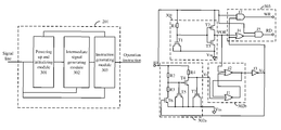
- FIG. 3 is a schematic structural diagram of an operation instruction generating circuit according to an embodiment of the present disclosure
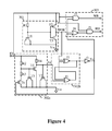
- FIG. 4 is a schematic diagram of an operation instruction generating circuit according to an embodiment of the present disclosure.
- FIG. 5 is a schematic diagram of an operation instruction generating circuit according to an embodiment of the present disclosure.
- FIG. 6 is a schematic diagram of an operation instruction generating circuit according to an embodiment of the present disclosure.
- FIG. 2 shows a schematic structural diagram of a consumable chip according to an embodiment.
- the consumable chip includes an operation instruction generating circuit 201 and a data storage circuit 202 .
- the operation instruction generating circuit 201 is configured to identify whether a signal transmitted through a signal line ID is a voltage source signal or a current source signal, i.e., whether the signal line ID is connected to a voltage source or a current source in the print imaging device. In a case that a voltage source signal is transmitted through the signal line ID, the operation instruction generating circuit 201 outputs a writing instruction WR. In a case that a current source signal is transmitted through the signal line ID, the operation instruction generating circuit 201 outputs a reading instruction RD.
- the operation instruction generation circuit 201 includes one input terminal for receiving the signal transmitted in the ID signal line and two output terminals.
- the two output terminals are respectively a reading instruction output terminal RD and a writing instruction output terminal WR, and hence, the operation instruction generating circuit is also referred to as a RD/WR identification circuit in the embodiment.
- the data storage circuit 202 is connected to the reading instruction output terminal RD and the writing instruction output terminal WR of the operation instruction generating circuit 201 .
- a memory which is easily programmed and erased for example, an EEPROM, a ferroelectric memory, a phase change memory or a flash memory
- a combination of a volatile memory and a power supply for example, an SRAM with a battery
- the data storage circuit 202 performs a data reading or a data writing operation on a target address of the data storage circuit 202 in response to the reading instruction or writing instruction received according to address information received (a transmission path of the address information is not show in FIG. 2 ).
- information stored in the data storage circuit 202 includes: identification information of a consumable cartridge, a manufacturer, a production date, ink usage, ink residual and toner colors.
- the information stored in the data storage circuit 202 may include only some of the information listed above or include other reasonable information not listed above, which is not limited in the present disclosure.
- a high level or a low level is outputted by the reading instruction output terminal RD and the writing instruction output terminal WR.
- a corresponding signal is defined as an active signal in a case that a high level is output.
- the reading instruction output terminal RD outputs a high level, it is indicated that the reading instruction is active.
- the writing instruction output terminal WR outputs a high level, it is indicated that the writing instruction is active.
- the two output terminals may be integrated into one output terminal within the operation instruction generating circuit 201 .
- the data storage circuit 202 only needs one input port to receive the reading instruction and the writing instruction, and it is not necessary to provide two ports to receive the reading instruction and the writing instruction respectively.
- a circuit structure of the data storage circuit simplified but also a process of analyzing and processing the reading instruction and the writing instruction by the data storage circuit is simplified, thereby improving reading/writing efficiency for data.
- the print imaging device In a case that the operation instruction generating circuit 201 outputs a high level at the reading instruction output terminal RD, it is indicated that the print imaging device needs to read data stored in the consumable chip.
- the print imaging device reads the data by collecting a voltage of the ID signal line.
- the data storage circuit 202 in the consumable chip outputs data at a target address in the data storage circuit 202 to the signal line ID based on the address information received, for the print imaging device to read information stored at a corresponding address in the consumable chip by collecting data transmitted through the signal line ID.
- the consumable chip determines an intention of the print imaging device based on the signal outputted via the signal line ID.
- the signal transmitted through the signal line ID is a current source signal
- the consumable chip determines that the print imaging device is to perform a reading operation.
- the signal transmitted through the signal line ID is a voltage source signal
- the consumable chip determines that the print imaging device is to perform a writing operation (for example, a programming operation).
- an operation instruction generating circuit shown in FIG. 3 is provided according to the embodiment.
- the operation instruction generating circuit 201 includes two main parts and a related peripheral circuit.
- One main part is a powering up and initializing module 301
- the other main part is a circuit composed of an intermediate signal generating module 302 and an instruction generating module 303 .
- the powering up and initializing module 301 is connected to a signal line ID, and can generate an initialized signal based on a signal transmitted through the signal line and transmit the initialized signal to the intermediate signal generating module 302 and the instruction generating module 303 .
- the intermediate signal generating module 302 is connected to the powering up and initializing module and the signal line ID, and can generate an intermediate signal based on the initialized signal and the signal transmitted through the signal line ID.
- the instruction generating module 303 is connected to the powering up and initializing module 301 , the intermediate signal generating module 302 and the signal line ID, and generates an operation instruction based on the initialized signal, the intermediate signal and the signal transmitted through the signal line ID.
- the operation instruction generated by the operation instruction generating circuit 201 includes a reading instruction and a writing instruction.
- FIG. 4 shows a specific schematic circuit diagram of the operation instruction generating circuit according to the embodiment.
- the powering up and initializing module 301 includes a resistor R 1 , a transistor T 1 functioning as a first energy storage unit, and a first phase inverter composed of a transistor T 2 and a transistor T 3 .
- the powering up and initializing module 301 can generate the initialized signal based on the signal transmitted through the signal line.
- the first energy storage unit and/or the first phase inverter may be implemented by other appropriate components or circuits, which is not limited in the present disclosure.
- the first energy storage unit may be a capacitor.
- the intermediate signal generating module 302 includes a first signal generating unit 302 a , a latch 302 b and a second phase inverter J 3 .
- An input terminal of the latch 302 b is connected to the first signal generating unit 302 a and the powering up and initializing module 301
- an input terminal of the second phase inverter J 3 is connected to an output terminal of the latch 302 b
- an output terminal of the second phase inverter J 3 is connected to the instruction generating module 303 and the first signal generating unit 302 a.
- the first signal generating unit 302 a includes a first resistor R 2 and a third resistor R 3 connected in series, a phase inverter composed of a first switch T 4 and a second resistor R 4 , a second switch T 6 for providing feedback, a transistor T 5 functioning as a second energy storage unit and a transistor T 7 functioning as a third energy storage unit.
- the first signal generating unit 302 a outputs a first signal Vr.
- the first switch T 4 and the second switch T 6 each are implemented by a transistor.
- the first switch, the second switch, the second energy storage unit and/or the third energy storage unit may be implemented by other appropriate components or circuits, which is not limited in the present disclosure.
- a control terminal (i.e., a grid) of the first switch i.e., the transistor T 4
- a first outreach terminal i.e., a source
- a second outreach terminal i.e., a drain
- a control terminal (i.e., a grid) of the second switch i.e., the transistor T 6
- a first outreach terminal i.e., a source
- a second outreach terminal i.e., a drain
- the second energy storage unit is connected between the control terminal and the second outreach terminal of the first switch T 4
- the third energy storage unit is connected between the first outreach terminal and the second outreach terminal of the first switch T 4 .
- a grid of the transistor T 5 functioning as the second energy storage unit is connected to the control terminal of the first switch T 4
- a source and a drain of the transistor T 5 are both connected to the ground Vss.
- a grid of the transistor T 7 functioning as the third energy storage unit is connected to the first outreach terminal of the first switch T 4 , and a source and a drain of the transistor T 7 are both connected to the ground Vss.
- the energy storage units may be other appropriate circuits or components (for example, capacitors) in replacement of the transistor T 5 and/or the transistor T 7 , which is not limited in the present disclosure.
- the instruction generating module 303 includes a first AND gate J 7 , a first NOR gate J 4 and a second AND gate J 5 .
- a first input terminal of the first AND gate J 7 is connected to the signal line ID, and a second input terminal of the first AND gate J 7 is connected to an output terminal of the second phase inverter J 3 .
- a first input terminal and a second input terminal of the first NOR gate J 4 are connected to the powering up and initializing module 301 and the output terminal of the second phase inverter J 3 respectively, and a first input terminal and a second input terminal of the second AND gate J 5 are connected to the signal line ID and the output terminal of the first NOR gate J 4 respectively.
- An initialized signal POR and the first signal Vr are outputted to an SR latch composed of the NOR gate J 1 and the NOR gate J 2 .
- An output of the latch is inverted by the second phase inverter (i.e., the NOT gate J 3 ) and then the second phase inverter outputs an intermediate signal Vc.
- the intermediate signal Vc is transmitted to the grid of the transistor T 6 .
- the intermediate signal Vc and the initialized signal POR are outputted to two input terminals of the first NOR gate J 4 respectively.
- Two input terminals of the second AND gate J 5 respectively receive an output of the first NOR gate J 4 and the signal transmitted through the signal line ID, and an output terminal RD of the second AND gate J 5 outputs a reading instruction.
- two input terminals of the first AND gate J 7 respectively receive the signal transmitted through the signal line ID and the intermediate signal Vc, and an output terminal WR of the first AND gate J 7 outputs a writing instruction.
- the resistor R 3 should meet the following conditions: a voltage distributed to the resistor R 3 by a current source does not reach a starting voltage of the transistor T 4 , in a case that the signal transmitted through the signal line ID is a current source signal and the transistor T 6 is switched on; and a voltage distributed to the resistor R 3 by a voltage source reaches or exceeds a starting voltage of the transistor T 5 , in a case that the signal transmitted through the signal line ID is a voltage source signal and the transistor T 6 is switched on.
- the operation instruction generating circuit performs powering up and initializing, as soon as the signal transmitted through the signal line ID is transmitted to the operation instruction generating circuit. Specifically, when the signal transmitted through the signal line ID is just transmitted to the operation instruction generating circuit, the signal transmitted through the signal line ID will charge the transistor T 5 since the transistor T 5 functions as a capacitor. In this case, the grid of the transistor T 4 is at a low level, and the transistor T 4 is thus not switched on. Similarly, since the transistor T 7 as well functions as a capacitor, in this case the first signal Vr outputted by the first signal generating unit 302 a is a low level signal.
- the inverter outputs a high level initialized signal POR.
- the SR latch composed of the NOR gate J 1 and the NOR gate J 2 initially outputs a low level signal to the NOT gate J 3 so that the intermediate signal Vc is a high level signal in an initial phase.
- the initialized signal POR discharges via the transistor T 3 and is restored to a low level. Since the intermediate signal Vc is a high level signal, the transistor T 6 is to be switched on.
- the operation instruction generating circuit 201 is configured to identify whether the signal transmitted through the signal line ID is a voltage source signal or a current source signal, i.e., whether the signal line ID is connected to a voltage source or a current source in the print imaging device. In a case that the signal transmitted through the signal line ID is a voltage source signal, the operation instruction generating circuit 201 outputs a writing instruction WR. In a case that the signal transmitted through the signal line ID is a current source signal, the operation instruction generating circuit 201 outputs a reading instruction RD.
- a resistance of the resistor R 3 should be smaller than 1.5 k ⁇ in a case that the signal transmitted through the signal line ID is a current source signal.
- the transistor T 6 is switched on. Since the resistance of the resistor R 3 is smaller than 1.5 k ⁇ and a current flowing through the resistor R 3 is 1 mA, a voltage distributed to the resistor R 3 (lower than 1.5V) is not sufficient to start the transistor T 4 . At this time, charging of the transistor T 7 functioning as a capacitor is completed, and thus the first signal Vr will be a high level signal.
- an output signal of the latch 302 b changes to a high level signal and the intermediate signal Vc outputted by the output terminal of the phase inverter J 3 is a low level signal. Since the initialized signal POR and the intermediate signal VC are both low level signals, the signal outputted by the NOR gate J 4 is a high level signal. It is easy to learn that the reading instruction output terminal RD outputs a high level and the writing instruction output terminal WR outputs a low level in this case, which indicates that the reading instruction is active.
- a ratio of a resistance of R 3 to that of R 2 should ensure that a voltage distributed to the resistor R 3 is higher than 1.5V (for example, the resistance of R 3 is 1 k ⁇ and the resistance of R 2 is 3 k ⁇ ) in a case that the signal transmitted through the signal line ID is a voltage source signal.
- the transistor T 6 is switched on, the voltage distributed to the resistor R 3 is 4V which is higher than the starting voltage of the transistor T 4 , and hence the transistor T 4 is switched on.
- the transistor T 4 is switched on, the transistor T 7 functioning as a capacitor discharges via the transistor T 4 , thereby restoring the first signal Vr to a low level.
- the initialized signal POR and the first signal Vr are both low level signals.
- the intermediate signal Vc maintains at a high level, and the NOR gate J 4 outputs a low level signal. It is easy to learn that the reading instruction output terminal RD outputs a low level signal and the writing instruction output terminal WR outputs a high level signal, which indicates that the writing instruction is active.
- a high level intermediate signal Vc may be outputted; or in a case that the signal transmitted through the signal line ID is a voltage source signal, a low level intermediate signal Vc may be outputted, which is not limited in the present disclosure.
- the instruction generating circuit outputs a high level signal at the reading instruction output terminal RD and outputs a low level signal at the writing instruction output terminal WR based on the high level intermediate signal Vc.
- the two output terminals may be integrated into one output terminal within the operation instruction generating circuit 201 , thereby simplifying the operation instruction generating circuit and reducing a volume and a cost of the circuit.
- the operation instruction generating circuit may have the circuit structure shown in FIG. 5 .
- a high level signal outputted by the circuit indicates a reading instruction
- a low level signal outputted by the circuit indicates a writing instruction.
- the operation instruction generating circuit may have the circuit structure show in FIG. 6 .
- a high level signal outputted by the circuit indicates a writing instruction
- a low level signal outputted by the circuit indicates a reading instruction.
- the operation instruction generating circuit can accurately determine an intention of the print imaging device based on a type of the signal transmitted through the signal line ID. That is, the operation instruction generating circuit can accurately generate a reading instruction in a case that the signal transmitted through the signal line ID is a current source signal; or the operating instruction generating circuit can accurately generate a writing instruction in a case that the signal transmitted through the signal line ID is a voltage source signal, thereby facilitating the consumable chip to respond to an action of the print imaging device timely and accurately.
- a non-volatile memory which can be rewritten easily does not directly apply to a print imaging device which is accessed via a voltage source and a current source
- the operation instruction generating circuit according to the embodiment can generate a corresponding operation instruction (for example, a reading instruction or a writing instruction) based on a voltage source signal or a current source signal so that the non-volatile memory which can be rewritten easily can be installed and used in the print imaging device.
Landscapes
- Engineering & Computer Science (AREA)
- Theoretical Computer Science (AREA)
- Chemical & Material Sciences (AREA)
- Crystallography & Structural Chemistry (AREA)
- Accessory Devices And Overall Control Thereof (AREA)
- Read Only Memory (AREA)
- Semiconductor Memories (AREA)
- Ink Jet (AREA)
Applications Claiming Priority (7)
| Application Number | Priority Date | Filing Date | Title |
|---|---|---|---|
| CN201410715520.0 | 2014-11-28 | ||
| CN201410715520 | 2014-11-28 | ||
| CN201410715520 | 2014-11-28 | ||
| CN201510317365.1A CN104943395B (zh) | 2014-11-28 | 2015-06-10 | 一种操作指令生成电路和耗材芯片 |
| CN201510317365 | 2015-06-10 | ||
| CN201510317365.1 | 2015-06-10 | ||
| PCT/CN2015/095537 WO2016082761A1 (zh) | 2014-11-28 | 2015-11-25 | 一种操作指令生成电路和耗材芯片 |
Publications (2)
| Publication Number | Publication Date |
|---|---|
| US20170330604A1 US20170330604A1 (en) | 2017-11-16 |
| US9865314B2 true US9865314B2 (en) | 2018-01-09 |
Family
ID=54158682
Family Applications (2)
| Application Number | Title | Priority Date | Filing Date |
|---|---|---|---|
| US15/528,925 Active US9865314B2 (en) | 2014-11-28 | 2015-11-25 | Operation instruction generating circuit and consumable chip |
| US15/122,722 Active US9633701B2 (en) | 2014-11-28 | 2015-11-25 | Resistor switching circuit, storage circuit, and consumable chip |
Family Applications After (1)
| Application Number | Title | Priority Date | Filing Date |
|---|---|---|---|
| US15/122,722 Active US9633701B2 (en) | 2014-11-28 | 2015-11-25 | Resistor switching circuit, storage circuit, and consumable chip |
Country Status (5)
| Country | Link |
|---|---|
| US (2) | US9865314B2 (es) |
| EP (1) | EP3109864B1 (es) |
| CN (2) | CN104952485B (es) |
| ES (1) | ES2735751T3 (es) |
| WO (2) | WO2016082761A1 (es) |
Families Citing this family (13)
| Publication number | Priority date | Publication date | Assignee | Title |
|---|---|---|---|---|
| CN104952485B (zh) * | 2014-11-28 | 2019-07-19 | 珠海艾派克微电子有限公司 | 一种电阻投切电路、存储电路以及耗材芯片 |
| CN113589045B (zh) * | 2018-01-17 | 2024-09-20 | 珠海极海半导体有限公司 | 敏感电阻测量装置及测量方法 |
| CN109263287B (zh) * | 2018-08-15 | 2020-01-31 | 珠海艾派克微电子有限公司 | Rc投切电路、电存储装置及印刷材料更换部件 |
| CN109334261B (zh) * | 2018-10-09 | 2023-12-29 | 杭州旗捷科技有限公司 | 指令生成电路、耗材芯片以及耗材 |
| CN112100117A (zh) * | 2019-06-18 | 2020-12-18 | 北京小米移动软件有限公司 | 电源复用电路、数据信号的切换方法及装置、电子设备 |
| CN112259138A (zh) * | 2019-07-22 | 2021-01-22 | 森富科技股份有限公司 | 内存装置 |
| CN111016465B (zh) * | 2019-12-24 | 2021-09-07 | 珠海艾派克微电子有限公司 | 一种芯片和成像盒 |
| CN111703210B (zh) * | 2019-12-31 | 2021-07-06 | 珠海艾派克微电子有限公司 | 耗材芯片和耗材芯片的响应方法、耗材盒及存储介质 |
| CN111806095B (zh) * | 2020-07-20 | 2021-09-07 | 珠海艾派克微电子有限公司 | 耗材余量检测方法、耗材及图像形成装置 |
| CN111817284B (zh) * | 2020-09-04 | 2021-01-19 | 深圳市永联科技股份有限公司 | 一种直流母线通信电路及方法 |
| CN113203921A (zh) * | 2020-11-26 | 2021-08-03 | 国网天津市电力公司 | 一键式支路间绝缘标准化全自动测试仪 |
| CN113110119B (zh) * | 2020-11-26 | 2022-08-19 | 国网天津市电力公司 | 一种电子式全自动支路交换器 |
| CN113848415A (zh) * | 2021-01-28 | 2021-12-28 | 江西理工大学 | Irf发生器、故障电阻的生成方法及irf注入方法 |
Citations (4)
| Publication number | Priority date | Publication date | Assignee | Title |
|---|---|---|---|---|
| CN1530233A (zh) | 2003-03-14 | 2004-09-22 | 林耕华 | 喷墨打印头的识别电路的烧录方法 |
| CN1749980A (zh) | 2000-06-30 | 2006-03-22 | 精工爱普生株式会社 | 打印材料容器的存取 |
| WO2010027470A2 (en) | 2008-09-04 | 2010-03-11 | Fb Sistemas S.A. | Printer cartridge microchip |
| CN104943395A (zh) | 2014-11-28 | 2015-09-30 | 珠海艾派克微电子有限公司 | 一种操作指令生成电路和耗材芯片 |
Family Cites Families (16)
| Publication number | Priority date | Publication date | Assignee | Title |
|---|---|---|---|---|
| JPH08235875A (ja) | 1994-12-27 | 1996-09-13 | Nkk Corp | 多値情報記憶装置およびその動作方法 |
| US5602925A (en) * | 1995-01-31 | 1997-02-11 | Etymotic Research, Inc. | Hearing aid with programmable resistor |
| US6655775B1 (en) * | 1996-10-15 | 2003-12-02 | Hewlett-Packard Development Company, L.P. | Method and apparatus for drop weight encoding |
| JP3133706B2 (ja) * | 1997-06-19 | 2001-02-13 | 三洋電機株式会社 | 不揮発性半導体メモリ装置 |
| US6655768B1 (en) * | 1999-10-04 | 2003-12-02 | Seiko Epson Corporation | Semiconductor integrated circuit, ink cartridge, and inkjet recording device |
| US20050062584A1 (en) * | 2003-09-24 | 2005-03-24 | Broadcom Corporation | High-linearity switched-resistor network for programmability |
| US7108357B2 (en) * | 2004-02-13 | 2006-09-19 | Hewlett-Packard Development Company, L.P. | Device identification using a programmable memory circuit |
| KR100725979B1 (ko) * | 2005-07-23 | 2007-06-08 | 삼성전자주식회사 | 비휘발성 메모리의 기입/독출 내구력 개선 장치 및 그 방법 |
| DE102005043489B4 (de) | 2005-09-13 | 2009-07-23 | Abb Ag | Automatisierungstechnische Einrichtung |
| DK2209645T3 (da) * | 2007-11-14 | 2013-05-13 | Hewlett Packard Development Co | Inkjet print-hoved med delte datalinjer |
| KR101047051B1 (ko) * | 2009-05-20 | 2011-07-06 | 주식회사 하이닉스반도체 | 비휘발성 반도체 메모리 회로 |
| US8284589B2 (en) * | 2010-08-20 | 2012-10-09 | Sandisk 3D Llc | Single device driver circuit to control three-dimensional memory element array |
| US8787068B2 (en) * | 2011-04-07 | 2014-07-22 | Elpida Memory, Inc. | Semiconductor device |
| CN202332456U (zh) | 2011-11-29 | 2012-07-11 | 上海贝岭股份有限公司 | 一种基于加权开关网络的数控变阻器 |
| KR20140080942A (ko) * | 2012-12-21 | 2014-07-01 | 에스케이하이닉스 주식회사 | 비휘발성 메모리 장치 |
| CN203191538U (zh) * | 2013-04-12 | 2013-09-11 | 昆明理工大学 | 二进制电阻数控电阻箱 |
-
2015
- 2015-06-10 CN CN201510317377.4A patent/CN104952485B/zh active Active
- 2015-06-10 CN CN201510317365.1A patent/CN104943395B/zh active Active
- 2015-11-25 WO PCT/CN2015/095537 patent/WO2016082761A1/zh not_active Ceased
- 2015-11-25 US US15/528,925 patent/US9865314B2/en active Active
- 2015-11-25 ES ES15863566T patent/ES2735751T3/es active Active
- 2015-11-25 EP EP15863566.4A patent/EP3109864B1/en active Active
- 2015-11-25 US US15/122,722 patent/US9633701B2/en active Active
- 2015-11-25 WO PCT/CN2015/095536 patent/WO2016082760A1/zh not_active Ceased
Patent Citations (7)
| Publication number | Priority date | Publication date | Assignee | Title |
|---|---|---|---|---|
| CN1749980A (zh) | 2000-06-30 | 2006-03-22 | 精工爱普生株式会社 | 打印材料容器的存取 |
| US7321436B2 (en) * | 2000-06-30 | 2008-01-22 | Seiko Epson Corporation | Access to printing material container |
| US20080106757A1 (en) | 2000-06-30 | 2008-05-08 | Noboru Asauchi | Access to printing material container |
| CN1530233A (zh) | 2003-03-14 | 2004-09-22 | 林耕华 | 喷墨打印头的识别电路的烧录方法 |
| WO2010027470A2 (en) | 2008-09-04 | 2010-03-11 | Fb Sistemas S.A. | Printer cartridge microchip |
| CN104943395A (zh) | 2014-11-28 | 2015-09-30 | 珠海艾派克微电子有限公司 | 一种操作指令生成电路和耗材芯片 |
| US20170069357A1 (en) | 2014-11-28 | 2017-03-09 | Apex Microelectronics Co., Ltd. | Resistor switching circuit, storage circuit, and consumable chip |
Non-Patent Citations (2)
| Title |
|---|
| International Search Report issued in PCT/CN2015/095537 dated Feb. 23, 2016, 3 pages. |
| PCT Written Opinion of the International Searching Authority issued in PCT/CN2015/095537 dated Feb. 23, 2016, 4 pages. |
Also Published As
| Publication number | Publication date |
|---|---|
| CN104943395B (zh) | 2016-08-31 |
| WO2016082760A1 (zh) | 2016-06-02 |
| CN104952485A (zh) | 2015-09-30 |
| CN104952485B (zh) | 2019-07-19 |
| EP3109864A4 (en) | 2017-07-26 |
| EP3109864B1 (en) | 2019-04-24 |
| US20170069357A1 (en) | 2017-03-09 |
| ES2735751T3 (es) | 2019-12-20 |
| EP3109864A1 (en) | 2016-12-28 |
| WO2016082761A1 (zh) | 2016-06-02 |
| US9633701B2 (en) | 2017-04-25 |
| US20170330604A1 (en) | 2017-11-16 |
| CN104943395A (zh) | 2015-09-30 |
Similar Documents
| Publication | Publication Date | Title |
|---|---|---|
| US9865314B2 (en) | Operation instruction generating circuit and consumable chip | |
| CN102166886B (zh) | 耗材芯片及其数据读写方法、耗材容器 | |
| US11250919B2 (en) | Voltage generation circuit which is capable of executing high-speed boost operation | |
| CN103879152B (zh) | 用于存储成像盒信息的盒芯片、成像盒及通信方法 | |
| CN104112478A (zh) | 集成电路和存储器件 | |
| CN103093810B (zh) | 电阻式存储器装置 | |
| CN104275939B (zh) | 耗材芯片及其数据写入方法、耗材容器 | |
| CN102529460A (zh) | 存储芯片及其在间隙供电时的充电控制方法、耗材容器、成像设备 | |
| US9013944B2 (en) | Auxiliary power device and user system including the same | |
| CN102509557B (zh) | 电可擦可编程只读存储器的数据擦写控制装置及方法、芯片及其数据写入方法、耗材容器 | |
| CN101031976B (zh) | 高功率效率存储器和卡 | |
| CN102509558B (zh) | 存储芯片及其充电方法 | |
| CN101947886A (zh) | 耗材芯片及耗材容器 | |
| CN104476923B (zh) | 耗材芯片及耗材容器、耗材芯片存储单元的供电方法 | |
| CN109346117A (zh) | Eeprom存储电路、eeprom存储芯片、耗材容器以及成像设备 | |
| US9734909B2 (en) | Non-volatile static random access memory | |
| US10147385B2 (en) | Online gamma adjustment system of liquid crystal | |
| CN216783086U (zh) | 一种耗材芯片、耗材盒及图像形成装置 | |
| CN109334261B (zh) | 指令生成电路、耗材芯片以及耗材 | |
| CN202395500U (zh) | 充电控制电路、耗材芯片及成像系统 | |
| US20110286281A1 (en) | Reference current generator used for programming and erasing of non-volatile memory | |
| CN121366618B (zh) | Nor Flash及其读操作模块、及其电源电路 | |
| CN102545334A (zh) | 充电控制电路和方法、耗材芯片及成像系统 | |
| JP2005190565A (ja) | 強誘電体メモリ装置、電子機器、及び駆動方法 | |
| CN202782180U (zh) | 耗材芯片及耗材容器 |
Legal Events
| Date | Code | Title | Description |
|---|---|---|---|
| AS | Assignment |
Owner name: APEX MICROELECTRONICS CO., LTD., CHINA Free format text: ASSIGNMENT OF ASSIGNORS INTEREST;ASSIGNORS:SUN, WANLI;WANG, XIONGWEI;XUE, RUYAN;AND OTHERS;REEL/FRAME:042572/0881 Effective date: 20170504 |
|
| STCF | Information on status: patent grant |
Free format text: PATENTED CASE |
|
| MAFP | Maintenance fee payment |
Free format text: PAYMENT OF MAINTENANCE FEE, 4TH YEAR, LARGE ENTITY (ORIGINAL EVENT CODE: M1551); ENTITY STATUS OF PATENT OWNER: LARGE ENTITY Year of fee payment: 4 |
|
| AS | Assignment |
Owner name: GEEHY MICROELECTRONICS INC., CHINA Free format text: CHANGE OF NAME;ASSIGNOR:APEX MICROELECTRONICS CO., LTD.;REEL/FRAME:062764/0046 Effective date: 20220921 |
|
| MAFP | Maintenance fee payment |
Free format text: PAYMENT OF MAINTENANCE FEE, 8TH YEAR, LARGE ENTITY (ORIGINAL EVENT CODE: M1552); ENTITY STATUS OF PATENT OWNER: LARGE ENTITY Year of fee payment: 8 |