US9933120B2 - LED screen display unit and production method therefor - Google Patents
LED screen display unit and production method therefor Download PDFInfo
- Publication number
- US9933120B2 US9933120B2 US14/760,315 US201414760315A US9933120B2 US 9933120 B2 US9933120 B2 US 9933120B2 US 201414760315 A US201414760315 A US 201414760315A US 9933120 B2 US9933120 B2 US 9933120B2
- Authority
- US
- United States
- Prior art keywords
- soldering
- circuit board
- pads
- led
- soldering pad
- Prior art date
- Legal status (The legal status is an assumption and is not a legal conclusion. Google has not performed a legal analysis and makes no representation as to the accuracy of the status listed.)
- Active, expires
Links
Images




Classifications
-
- F—MECHANICAL ENGINEERING; LIGHTING; HEATING; WEAPONS; BLASTING
- F21—LIGHTING
- F21K—NON-ELECTRIC LIGHT SOURCES USING LUMINESCENCE; LIGHT SOURCES USING ELECTROCHEMILUMINESCENCE; LIGHT SOURCES USING CHARGES OF COMBUSTIBLE MATERIAL; LIGHT SOURCES USING SEMICONDUCTOR DEVICES AS LIGHT-GENERATING ELEMENTS; LIGHT SOURCES NOT OTHERWISE PROVIDED FOR
- F21K9/00—Light sources using semiconductor devices as light-generating elements, e.g. using light-emitting diodes [LED] or lasers
- F21K9/20—Light sources comprising attachment means
-
- F21K9/30—
-
- F—MECHANICAL ENGINEERING; LIGHTING; HEATING; WEAPONS; BLASTING
- F21—LIGHTING
- F21K—NON-ELECTRIC LIGHT SOURCES USING LUMINESCENCE; LIGHT SOURCES USING ELECTROCHEMILUMINESCENCE; LIGHT SOURCES USING CHARGES OF COMBUSTIBLE MATERIAL; LIGHT SOURCES USING SEMICONDUCTOR DEVICES AS LIGHT-GENERATING ELEMENTS; LIGHT SOURCES NOT OTHERWISE PROVIDED FOR
- F21K9/00—Light sources using semiconductor devices as light-generating elements, e.g. using light-emitting diodes [LED] or lasers
- F21K9/90—Methods of manufacture
-
- F—MECHANICAL ENGINEERING; LIGHTING; HEATING; WEAPONS; BLASTING
- F21—LIGHTING
- F21V—FUNCTIONAL FEATURES OR DETAILS OF LIGHTING DEVICES OR SYSTEMS THEREOF; STRUCTURAL COMBINATIONS OF LIGHTING DEVICES WITH OTHER ARTICLES, NOT OTHERWISE PROVIDED FOR
- F21V23/00—Arrangement of electric circuit elements in or on lighting devices
- F21V23/003—Arrangement of electric circuit elements in or on lighting devices the elements being electronics drivers or controllers for operating the light source, e.g. for a LED array
- F21V23/004—Arrangement of electric circuit elements in or on lighting devices the elements being electronics drivers or controllers for operating the light source, e.g. for a LED array arranged on a substrate, e.g. a printed circuit board
- F21V23/005—Arrangement of electric circuit elements in or on lighting devices the elements being electronics drivers or controllers for operating the light source, e.g. for a LED array arranged on a substrate, e.g. a printed circuit board the substrate is supporting also the light source
-
- H—ELECTRICITY
- H05—ELECTRIC TECHNIQUES NOT OTHERWISE PROVIDED FOR
- H05K—PRINTED CIRCUITS; CASINGS OR CONSTRUCTIONAL DETAILS OF ELECTRIC APPARATUS; MANUFACTURE OF ASSEMBLAGES OF ELECTRICAL COMPONENTS
- H05K1/00—Printed circuits
- H05K1/18—Printed circuits structurally associated with non-printed electric components
-
- H—ELECTRICITY
- H05—ELECTRIC TECHNIQUES NOT OTHERWISE PROVIDED FOR
- H05K—PRINTED CIRCUITS; CASINGS OR CONSTRUCTIONAL DETAILS OF ELECTRIC APPARATUS; MANUFACTURE OF ASSEMBLAGES OF ELECTRICAL COMPONENTS
- H05K3/00—Apparatus or processes for manufacturing printed circuits
- H05K3/30—Assembling printed circuits with electric components, e.g. with resistors
- H05K3/32—Assembling printed circuits with electric components, e.g. with resistors electrically connecting electric components or wires to printed circuits
- H05K3/328—Assembling printed circuits with electric components, e.g. with resistors electrically connecting electric components or wires to printed circuits by welding
-
- H—ELECTRICITY
- H05—ELECTRIC TECHNIQUES NOT OTHERWISE PROVIDED FOR
- H05K—PRINTED CIRCUITS; CASINGS OR CONSTRUCTIONAL DETAILS OF ELECTRIC APPARATUS; MANUFACTURE OF ASSEMBLAGES OF ELECTRICAL COMPONENTS
- H05K3/00—Apparatus or processes for manufacturing printed circuits
- H05K3/40—Forming printed elements for providing electric connections to or between printed circuits
- H05K3/403—Edge contacts; Windows or holes in the substrate having plural connections on the walls thereof
-
- F—MECHANICAL ENGINEERING; LIGHTING; HEATING; WEAPONS; BLASTING
- F21—LIGHTING
- F21Y—INDEXING SCHEME ASSOCIATED WITH SUBCLASSES F21K, F21L, F21S and F21V, RELATING TO THE FORM OR THE KIND OF THE LIGHT SOURCES OR OF THE COLOUR OF THE LIGHT EMITTED
- F21Y2115/00—Light-generating elements of semiconductor light sources
- F21Y2115/10—Light-emitting diodes [LED]
-
- G—PHYSICS
- G09—EDUCATION; CRYPTOGRAPHY; DISPLAY; ADVERTISING; SEALS
- G09F—DISPLAYING; ADVERTISING; SIGNS; LABELS OR NAME-PLATES; SEALS
- G09F9/00—Indicating arrangements for variable information in which the information is built-up on a support by selection or combination of individual elements
- G09F9/30—Indicating arrangements for variable information in which the information is built-up on a support by selection or combination of individual elements in which the desired character or characters are formed by combining individual elements
- G09F9/33—Indicating arrangements for variable information in which the information is built-up on a support by selection or combination of individual elements in which the desired character or characters are formed by combining individual elements being semiconductor devices, e.g. diodes
-
- H—ELECTRICITY
- H05—ELECTRIC TECHNIQUES NOT OTHERWISE PROVIDED FOR
- H05K—PRINTED CIRCUITS; CASINGS OR CONSTRUCTIONAL DETAILS OF ELECTRIC APPARATUS; MANUFACTURE OF ASSEMBLAGES OF ELECTRICAL COMPONENTS
- H05K2201/00—Indexing scheme relating to printed circuits covered by H05K1/00
- H05K2201/09—Shape and layout
- H05K2201/09145—Edge details
- H05K2201/09163—Slotted edge
-
- H—ELECTRICITY
- H05—ELECTRIC TECHNIQUES NOT OTHERWISE PROVIDED FOR
- H05K—PRINTED CIRCUITS; CASINGS OR CONSTRUCTIONAL DETAILS OF ELECTRIC APPARATUS; MANUFACTURE OF ASSEMBLAGES OF ELECTRICAL COMPONENTS
- H05K2201/00—Indexing scheme relating to printed circuits covered by H05K1/00
- H05K2201/09—Shape and layout
- H05K2201/09145—Edge details
- H05K2201/09181—Notches in edge pads
-
- H—ELECTRICITY
- H05—ELECTRIC TECHNIQUES NOT OTHERWISE PROVIDED FOR
- H05K—PRINTED CIRCUITS; CASINGS OR CONSTRUCTIONAL DETAILS OF ELECTRIC APPARATUS; MANUFACTURE OF ASSEMBLAGES OF ELECTRICAL COMPONENTS
- H05K2201/00—Indexing scheme relating to printed circuits covered by H05K1/00
- H05K2201/10—Details of components or other objects attached to or integrated in a printed circuit board
- H05K2201/10007—Types of components
- H05K2201/10106—Light emitting diode [LED]
-
- H—ELECTRICITY
- H05—ELECTRIC TECHNIQUES NOT OTHERWISE PROVIDED FOR
- H05K—PRINTED CIRCUITS; CASINGS OR CONSTRUCTIONAL DETAILS OF ELECTRIC APPARATUS; MANUFACTURE OF ASSEMBLAGES OF ELECTRICAL COMPONENTS
- H05K2201/00—Indexing scheme relating to printed circuits covered by H05K1/00
- H05K2201/10—Details of components or other objects attached to or integrated in a printed circuit board
- H05K2201/10431—Details of mounted components
- H05K2201/10439—Position of a single component
- H05K2201/10446—Mounted on an edge
-
- H—ELECTRICITY
- H05—ELECTRIC TECHNIQUES NOT OTHERWISE PROVIDED FOR
- H05K—PRINTED CIRCUITS; CASINGS OR CONSTRUCTIONAL DETAILS OF ELECTRIC APPARATUS; MANUFACTURE OF ASSEMBLAGES OF ELECTRICAL COMPONENTS
- H05K3/00—Apparatus or processes for manufacturing printed circuits
- H05K3/30—Assembling printed circuits with electric components, e.g. with resistors
- H05K3/32—Assembling printed circuits with electric components, e.g. with resistors electrically connecting electric components or wires to printed circuits
- H05K3/34—Assembling printed circuits with electric components, e.g. with resistors electrically connecting electric components or wires to printed circuits by soldering
- H05K3/3405—Edge mounted components, e.g. terminals
-
- Y—GENERAL TAGGING OF NEW TECHNOLOGICAL DEVELOPMENTS; GENERAL TAGGING OF CROSS-SECTIONAL TECHNOLOGIES SPANNING OVER SEVERAL SECTIONS OF THE IPC; TECHNICAL SUBJECTS COVERED BY FORMER USPC CROSS-REFERENCE ART COLLECTIONS [XRACs] AND DIGESTS
- Y10—TECHNICAL SUBJECTS COVERED BY FORMER USPC
- Y10T—TECHNICAL SUBJECTS COVERED BY FORMER US CLASSIFICATION
- Y10T29/00—Metal working
- Y10T29/49—Method of mechanical manufacture
- Y10T29/49002—Electrical device making
- Y10T29/49117—Conductor or circuit manufacturing
- Y10T29/49124—On flat or curved insulated base, e.g., printed circuit, etc.
- Y10T29/4913—Assembling to base an electrical component, e.g., capacitor, etc.
Definitions
- the present disclosure relates to the field of display screens, and in particular to a display unit for a Light-Emitting Diode (LED) screen and a production method therefor.
- LED Light-Emitting Diode
- the LED screen has been widely used.
- the LED screen is required to have a hollow structure, which is advantageous for: (1) not obstructing vision, so that objects in front of and behind the LED screen are visible; (2) a certain permeability of light, to meet indoor light requirements for a glass curtain wall or shop window employing the LED screens; (3) a mostly reduced impact on the overall decoration design in the scenario employing the LED screens; and (4) a certain artistic effect, especially in the case of a stage performance, to achieve a fancy effect that the displayed image is visible but the screen is invisible.
- the hollow LED screen is particularly popular in some special scenarios such as airports, hotels, buildings with glass curtain wall, exhibition centers, performance stages and shop windows, and has an application effect much better than the conventional box-type LED screen.
- Both permeability of light and a pixel resolution are considered in designing the hollow LED screen, and under the same design conditions, the higher pixel resolution means the lower aperture ratio, which results in the worse permeability of light.
- Typical relations between pixel pitches and the corresponding pixel resolutions of the LED screen are listed in a table below:
- pixel pitch (P) pixel resolution (R) 40 mm 625 pixels/m 2 25 mm 1600 pixels/m 2 20 mm 2500 pixels/m 2 16 mm 3906 pixels/m 2 10 mm 10000 pixels/m 2 8 mm 15625 pixels/m 2 7 mm 20408 pixels/m 2 6 mm 27777 pixels/m 2 5 mm 40000 pixels/m 2 * Note: the pixel resolution R is calculated by a formula: R (1000 mm ⁇ 1000 mm)/(P ⁇ P).
- soldering pads of the display unit are disposed on an upper surface of a circuit board, so that LED lights welded on the soldering pads are located on the upper surface of the circuit board, thus the LED lights block light, and such structure reduces the permeability of light through the LED screen. Therefore, a high permeability of light cannot be ensured in the case of a high pixel resolution in the LED screen in the prior art.
- An object of the present disclosure is to propose a display unit for LED screen, which can ensure a high permeability of light in the case of a high pixel resolution in the LED screen.
- a display unit for LED screen including a circuit board, a driving IC and an LED light, a soldering pad matrix is provided on a first lateral surface of the circuit board, the driving IC is arranged on the circuit board and electrically connected to soldering pads of the soldering pad matrix, and pins of the LED light are welded to the soldering pads of the soldering pad matrix.
- the soldering pad matrix is composed of a set of soldering pads located on an upper half of the first lateral surface and another set of soldering pads located on a lower half of the first lateral surface, the set of soldering pads located on the upper half of the first lateral surface respectively correspond to and are separated from the another set of soldering pads located on the lower half of the first lateral surface, and a height of each bonding pad is 30-45% of a thickness of the circuit board.
- a V-shaped groove is horizontally extended in the middle of the first lateral surface of the circuit board.
- the display unit for LED screen includes at least two said bondage pad matrixes, which are equally spaced on the first lateral surface of the circuit board, and corresponding to the soldering pad matrixes, there are at least two said LED lights which are also equally spaced on the first lateral surface of the circuit board.
- the LED light has four or six pins, and corresponding to the number of the pins of the LED light, the soldering pad matrix has four or six soldering pads which are flat.
- a method for producing the previous display unit for LED screen including:
- Step 1 arranging a soldering pad matrix on a first lateral surface of a circuit board
- Step 2 arranging a driving IC on the circuit board and electrically connecting the driving IC to soldering pads of the soldering pad matrix;
- Step 3 welding pins of an LED light to the bonding pad of the soldering pad matrix.
- the Step 1 specifically includes:
- the Step 3 further includes:
- the Step 1 further includes:
- At least two said bonding pad matrixes are arranged in the Step 1, and are equally spaced on the first lateral surface of the circuit board, and corresponding to the soldering pad matrix, at least two LED lights are arranged in the Step 3, and are equally spaced on the first lateral surface of the circuit board.
- the LED light has four or six pins in the Step 3, and corresponding to the number of the pins of the LED light, the soldering pad matrix has four or six soldering pads which are flat in the Step 1.
- the present disclosure has the following advantages that: since the soldering pad matrixes are formed on the lateral surface of the circuit board, LED lights can be automatically surface-mounted onto the soldering pad matrixes on the lateral surface; and the LED lights will not block light, so that the permeability of light is high in the case of a high pixel resolution in the the LED screen employing the display units. Further, the method of the present disclosure allows automatic mass production of the display unit for LED screen at a high production efficiency.
- FIG. 1 is a partial structural diagram of a display unit for LED screen according to the present disclosure
- FIG. 2 is an enlarged view of a soldering pad matrix of the display unit for LED screen according to the present disclosure
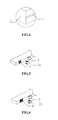
- FIG. 3 is a schematic view of a V-shaped groove at a first lateral surface of the display unit for LED screen according to the present disclosure
- FIG. 4 is an enlarged view of a part indicated by I in FIG. 3 ;
- FIG. 5 is a partial structural diagram of the display unit for LED screen, on which an LED light with four pins is mounted, according to the present disclosure
- FIG. 6 is a partial structural diagram of the display unit for LED screen, on which an LED light with six pins is mounted, according to the present disclosure
- FIG. 7 is an overall view of the display unit for LED screen according to the present disclosure.
- FIG. 8 is a flow chart of a production method for the display unit for LED screen according to the present disclosure.
- FIG. 9A is a flow chart of forming a soldering pad matrix of the display unit for LED screen according to the present disclosure.
- FIG. 9B is a flow chart of mounting an LED light on the display unit for LED screen according to the present disclosure.
- FIG. 10A is a schematic view showing an operation of Step 101 of the production method for the display unit for LED screen according to the present disclosure
- FIG. 10B is a schematic view showing an operation of Step 301 of the production method for the display unit for LED screen according to the present disclosure
- FIG. 10C is a schematic view showing an operation of Step 304 of the production method for the display unit for LED screen according to the present disclosure.
- FIG. 11 is a flow chart of forming another soldering pad matrix in the production method for the display unit for LED screen according to the present disclosure.
- Circuit board 2. Driving Integrated Circuit (IC) 3. LED light 31. Pin 4. Bonding pad 41. Bonding pad matrix 42. Waist-shaped hole 43. Boundary of first lateral surface 5. V-shaped groove
- a first embodiment of the present disclosure provides a display unit for LED screen, as shown in FIGS. 1 and 2 .
- the display unit for LED screen includes a circuit board 1 , a driving IC 2 and LED lights 3 .
- soldering pad matrixes 41 are provided on a first lateral surface of the circuit board 1
- the driving IC 2 is arranged on the circuit board 1 and electrically connected to soldering pads 4 of the soldering pad matrixes 41
- pins 31 of the LED lights 3 are welded to the soldering pads 4 of the soldering pad matrixes 41 .
- the LED screen employing the display unit has a high permeability of light, and meanwhile the LED lights 3 can be automatically surface-mounted on the soldering pad matrixes 41 , thereby improving the production efficiency and reducing labor costs.
- Each of the soldering pad matrixes 41 is composed of a set of soldering pads 4 located on the upper half of the first lateral surface of the circuit board 1 and another set of soldering pads 4 located on the lower half of the first lateral surface of the circuit board 1 , the set of soldering pads 4 located on the upper half of the first lateral surface respectively correspond to and are separated from the another set of soldering pads 4 located on the lower half of the first lateral surface, and a height of each bonding pad 4 is 30-45% of the thickness of the circuit board 1 .
- the upper half and the lower half are described herein referring to the orientation as shown in FIG. 1 , and the height of the bonding pad 4 refers to a length of the bonding pad 4 in a direction perpendicular to a first main surface (i.e. the upper surface or the lower surface) of the circuit board 1 .
- the height of each bonding pad 4 being about 30-45% of the thickness of the circuit board 1 means that an insulation portion having a height of about 10-40% of the thickness of the circuit board 1 is present between the two sets of soldering pads 4 .
- the insulation portion can separate the soldering pads 4 located at the upper half from the soldering pads 4 located at the lower half on the first lateral surface, while ensuring that the soldering pads 4 are big enough to be welded with the pins 31 of the LED light 3 .
- FIGS. 3 and 4 A preferable implementation of the display unit for LED screen according to the disclosure is shown in FIGS. 3 and 4 .
- a V-shaped groove 5 is horizontally extended in the middle of the first lateral surface of the circuit board 1 .
- the arrangement of the V-shaped groove 5 on the first lateral surface of the circuit board 1 is preferred to form the sets of soldering pads 4 , which are separated from each other, on the upper and lower halves of the first lateral surface of the circuit board 1 .
- the arranged soldering pads 4 are electrically insulated by the V-shaped groove 5 added as an insulation portion which is clearly visible, thus operations are simple, implementation is convenient and a processing efficiency is high. Further, the design of the V-shaped groove 5 facilitates the forming of the soldering pad matrix 41 on the first lateral surface.
- FIGS. 5 to 7 Another preferable implementation of the display unit for LED screen according to the disclosure is shown in FIGS. 5 to 7 .
- bonding pad matrixes 41 which are equally spaced on the first lateral surface of the circuit board 1 .
- LED lights 3 which are also equally spaced on the first lateral surface of the circuit board 1 .
- the at least two soldering pad matrixes 41 allow mounting of many LED lights 3 on each circuit board 1 , and the even arrangement of the soldering pad matrixes 41 can ensure the even arrangement of the LED lights 3 in the LED screen, so that the assembly of the LED screen is simpler. Meanwhile, the overall display effect of the LED screen can be ideal if the LED lights 3 functioning as pixels in the LED screen are evenly distributed.
- the LED light 3 has four or six pins 31 .
- the soldering pad matrix 41 also has four or six soldering pads 4 which are flat.
- the soldering pad matrix 41 having four or six soldering pads 4 can well suit to the packaged LED lights 3 with four or six pins 31 which are currently available on the market.
- the flat bonding pad is beneficial for surface mounting of the LED lights 3 .
- FIG. 8 A first implementation of a method for producing the above-described display unit for LED screen according to the disclosure is shown in FIG. 8 , and the method includes:
- Step 1 arranging a soldering pad matrix 41 on a first lateral surface of a circuit board 1 ;
- Step 2 arranging a driving IC 2 on the circuit board 1 and electrically connecting the driving IC 2 to soldering pads 4 of the soldering pad matrix 41 ;
- Step 3 welding pins 31 of an LED light 3 to the soldering pads 4 of the soldering pad matrix 41 .
- the above three Steps 1 to 3 can achieve the automated production of the display unit for LED screen, thereby improving the production efficiency.
- arranging the soldering pad matrix 41 on the first lateral surface of the circuit board 1 specifically includes:
- Step 101 drilling two or more equally-spaced sets of waist-shaped holes (i.e. elliptic holes) 42 on a first main surface of a jointed board for making the circuit board 1 along a boundary 43 of the first lateral surface of the circuit board 1 , where the depth of each of the waist-shaped holes 42 is 30-45% of a thickness of the circuit board 1 ;
- waist-shaped holes i.e. elliptic holes
- Step 102 drilling sets of waist-shaped holes 42 at positions on a second main surface of the jointed board which respectively correspond to the sets of waist-shaped holes 42 on the first main surface, where the depth of each of the waist-shaped holes 42 on the second main surface is 30-45% of the thickness of the circuit board 1 ;
- Step 103 metallizing the waist-shaped holes 42 ;
- Step 104 cutting the jointed board along the boundary 43 of the first lateral surface, so that a soldering pad matrix 41 is formed by a set of waist-shaped holes 42 on the first main surface and a set of waist-shaped holes 42 on the second main surface due to the cutting.
- welding the pins 31 of the LED light 3 to the soldering pads 4 of the soldering pad matrix 41 specifically includes:
- Step 301 orienting the first lateral surface of the circuit board 1 upward;
- Step 302 placing a steel mesh so that openings of the steel mesh correspond to the soldering pads 4 , respectively;
- Step 303 applying solder paste on the soldering pads 4 through the openings of the steel mesh;
- Step 304 automatically surface-mounting the LED lights 3 on the soldering pads 4 applied with the solder paste.
- Step 305 passing the soldering pads 4 on which the LED lights 3 are automatically surface-mounted through a reflow soldering high-temperature tin stove.
- Step 101 The operation of Step 101 is schematically shown in FIG. 10A
- the implementation of Step 301 is shown in FIG. 10B
- the operation of Step 304 is schematically shown in FIG. 10C .
- the soldering pad matrixes 41 can be efficiently and accurately formed on the lateral surface of the circuit board 1 according to the disclosure.
- each LED light 3 is manually welded onto the soldering pad matrix 41 , leading to a low work efficiency and a high error rate.
- the pins 31 of the LED light 3 can be attached to the soldering pads 4 of the soldering pad matrix 41 efficiently and quickly in an automatic production manner, thereby improving the production efficiency and the qualified rate of products.
- FIG. 11 Another preferable implementation of the method for producing the display unit for LED screen of the present disclosure is shown in FIG. 11 , and the method includes:
- Step 401 drilling two or more equally-spaced sets of waist-shaped holes (i.e. elliptic holes) 42 on a first main surface of a jointed board for making the circuit board 1 along a boundary 43 of the first lateral surface of the circuit board 1 , where the waist-shaped holes 42 penetrate through the circuit board 1 ;
- waist-shaped holes i.e. elliptic holes
- Step 402 metallizing the waist-shaped holes 42 ;
- Step 403 cutting the jointed board along the boundary 43 of the first lateral surface
- Step 404 horizontally forming a V-shaped groove 5 in the middle of the first lateral surface, to form a soldering pad matrix 41 on the first lateral surface.
- the arrangement of the V-shaped groove 5 facilitates the quick forming of the soldering pad matrixes 41 .
- At least two bonding pad matrixes 41 are arranged in Step 1, and are equally spaced on the first lateral surface of the circuit board 1 .
- at least two LED lights 3 are arranged in Step 3, and are equally spaced on the first lateral surface of the circuit board 1 .
- the LED light 3 has four or six pins 31 .
- the soldering pad matrix 41 has four or six soldering pads 4 which are flat.
- the at least two soldering pad matrixes 41 allow mounting of many LED lights 3 on each circuit board 1 , and the even arrangement of the soldering pad matrixes 41 can ensure the even arrangement of the LED lights 3 in the LED screen, so that the assembly of the LED screen is simpler. Meanwhile, the overall display effect of the LED screen can be ideal if the LED lights 3 functioning as pixels in the LED screen are evenly distributed.
- the soldering pad matrixes 41 having four or six soldering pads 4 can well suit to the packaged LED lights 3 with four or six pins 31 which are currently available on the market.
- the flat bonding pad is beneficial for surface mounting of the LED lights 3 .
Landscapes
- Engineering & Computer Science (AREA)
- Microelectronics & Electronic Packaging (AREA)
- General Engineering & Computer Science (AREA)
- Manufacturing & Machinery (AREA)
- Physics & Mathematics (AREA)
- Optics & Photonics (AREA)
- Devices For Indicating Variable Information By Combining Individual Elements (AREA)
- Led Device Packages (AREA)
- General Physics & Mathematics (AREA)
- Theoretical Computer Science (AREA)
Applications Claiming Priority (4)
| Application Number | Priority Date | Filing Date | Title |
|---|---|---|---|
| CN201310011178 | 2013-01-11 | ||
| CN201310011178.1A CN103065560B (zh) | 2013-01-11 | 2013-01-11 | 一种led显示屏显示单元及其生产方法 |
| CN201310011178.1 | 2013-01-11 | ||
| PCT/CN2014/070312 WO2014108070A1 (fr) | 2013-01-11 | 2014-01-08 | Unité d'affichage de type écran à del et procédé de production de ladite unité d'affichage |
Publications (2)
| Publication Number | Publication Date |
|---|---|
| US20150362133A1 US20150362133A1 (en) | 2015-12-17 |
| US9933120B2 true US9933120B2 (en) | 2018-04-03 |
Family
ID=48108169
Family Applications (1)
| Application Number | Title | Priority Date | Filing Date |
|---|---|---|---|
| US14/760,315 Active 2034-04-27 US9933120B2 (en) | 2013-01-11 | 2014-01-08 | LED screen display unit and production method therefor |
Country Status (7)
| Country | Link |
|---|---|
| US (1) | US9933120B2 (fr) |
| EP (1) | EP2945146B1 (fr) |
| JP (1) | JP6211097B2 (fr) |
| KR (1) | KR101780135B1 (fr) |
| CN (1) | CN103065560B (fr) |
| ES (1) | ES2736282T3 (fr) |
| WO (1) | WO2014108070A1 (fr) |
Families Citing this family (16)
| Publication number | Priority date | Publication date | Assignee | Title |
|---|---|---|---|---|
| CN103065560B (zh) * | 2013-01-11 | 2015-09-09 | 深圳市晶泓科技有限公司 | 一种led显示屏显示单元及其生产方法 |
| CN104394644A (zh) * | 2014-10-24 | 2015-03-04 | 苏州德鲁森自动化系统有限公司 | 一种四引脚3528led灯的焊盘 |
| CN104537960B (zh) * | 2014-12-24 | 2018-01-23 | 深圳市晶泓达光电工程技术有限公司 | 一种led显示模块及其制备方法 |
| CN104537959B (zh) * | 2014-12-24 | 2017-10-27 | 深圳市晶泓达光电工程技术有限公司 | 一种led显示模块及其制备方法 |
| CN104979326B (zh) * | 2015-07-09 | 2017-12-05 | 深圳市晶泓科技有限公司 | Led发光组件、led发光面板和led显示屏 |
| CN105180101B (zh) * | 2015-07-27 | 2018-04-10 | 深圳市赫尔诺电子技术有限公司 | 在pcb板的侧面上贴装led灯珠的方法 |
| CN106157829B (zh) * | 2016-06-28 | 2020-05-05 | 南京华立得电子有限公司 | 一种led数码管安装构件及其led幕墙 |
| US10514131B2 (en) * | 2016-07-06 | 2019-12-24 | Epistar Corporation | Light-emitting apparatus |
| CN106968391A (zh) * | 2016-10-27 | 2017-07-21 | 厦门腾月光电科技有限公司 | 发光建材 |
| CN106710460A (zh) * | 2017-02-07 | 2017-05-24 | 西安青松光电技术有限公司 | 一种透明led显示屏显示单元及其制备方法 |
| CN109310012B (zh) * | 2018-07-19 | 2024-08-30 | 广州市建筑科学研究院有限公司 | 一种钢网及使用该钢网的手工回流焊接方法 |
| JP6623356B1 (ja) * | 2019-05-23 | 2019-12-25 | 合同会社jujube | 電子部品の実装構造及び電子部品の実装方法 |
| CN110390890A (zh) * | 2019-08-01 | 2019-10-29 | 深圳市恒利普智能显示有限公司 | 灯条和灯条的制作方法 |
| JP7180619B2 (ja) * | 2020-01-10 | 2022-11-30 | Tdk株式会社 | 電子部品及びその製造方法 |
| CN111757611B (zh) * | 2020-06-05 | 2021-12-31 | 深圳市隆利科技股份有限公司 | 一种应用于miniLED的安装结构及其制作方法 |
| CN112996239A (zh) * | 2021-03-04 | 2021-06-18 | 江西志浩电子科技有限公司 | 一种侧边带smt焊盘的pcb板及制备方法 |
Citations (12)
| Publication number | Priority date | Publication date | Assignee | Title |
|---|---|---|---|---|
| US6069644A (en) * | 1996-02-20 | 2000-05-30 | Canon Kabushiki Kaisha | Recording head and image forming apparatus using the same |
| US6198093B1 (en) * | 1998-11-19 | 2001-03-06 | Xerox Corporation | Electro optical devices with reduced filter thinning on the edge pixel photosites and method of producing same |
| CN101368701A (zh) | 2008-09-23 | 2009-02-18 | 北京中庆微数字设备开发有限公司 | 一种led单元和led装置 |
| CN101377272A (zh) | 2008-09-28 | 2009-03-04 | 北京中庆微数字设备开发有限公司 | 一种led装置 |
| CN101392878A (zh) | 2008-10-15 | 2009-03-25 | 北京中庆微数字设备开发有限公司 | 一种led灯条和led屏体 |
| CN101599239A (zh) | 2009-05-27 | 2009-12-09 | 幸琳 | 一种led显示装置和led显示屏箱体 |
| CN101814260A (zh) | 2009-12-23 | 2010-08-25 | 北京巨数数字技术开发有限公司 | 一种轻薄led显示屏和led显示系统 |
| US20110037079A1 (en) * | 2009-08-11 | 2011-02-17 | Provision Business & Technology Consulting Services, Inc. | Structure and method for fabricating fluorescent powder gel light emitting module |
| CN103065560A (zh) | 2013-01-11 | 2013-04-24 | 林谊 | 一种led显示屏显示单元及其生产方法 |
| CN103065561A (zh) | 2013-01-11 | 2013-04-24 | 林谊 | 一种led显示屏显示单元及其自动化生产方法 |
| CN203070686U (zh) | 2013-01-11 | 2013-07-17 | 深圳市晶泓科技有限公司 | 一种led显示屏显示单元 |
| CN203070687U (zh) | 2013-01-11 | 2013-07-17 | 深圳市晶泓科技有限公司 | 一种led显示屏显示单元 |
Family Cites Families (18)
| Publication number | Priority date | Publication date | Assignee | Title |
|---|---|---|---|---|
| JPH065470B2 (ja) * | 1986-03-31 | 1994-01-19 | タキロン株式会社 | 発光表示体パネル |
| JPH085508Y2 (ja) * | 1990-09-26 | 1996-02-14 | 三洋電機株式会社 | 発光ダイオード表示装置 |
| JPH0573677U (ja) * | 1992-03-04 | 1993-10-08 | エムケー精工株式会社 | 発光ダイオード表示装置 |
| JPH1078758A (ja) * | 1996-09-05 | 1998-03-24 | Yaskawa Electric Corp | 表示装置 |
| KR100314494B1 (ko) * | 1998-02-05 | 2001-11-15 | 가노 다다오 | 광원장치 및 표시장치 |
| US6677918B2 (en) * | 2001-09-21 | 2004-01-13 | Yuji Yuhara | Light emitting diode display system |
| US20050052863A1 (en) * | 2003-09-10 | 2005-03-10 | Seongukk Kim | Structure for engaging light emitting diode of rotational information display device |
| CN2731254Y (zh) * | 2004-09-20 | 2005-10-05 | 樊邦弘 | 一种条灯的改良结构 |
| JP3977837B2 (ja) * | 2004-12-27 | 2007-09-19 | 株式会社韓国サイン | Ledを用いたブラインド型の表示装置 |
| US7777699B2 (en) * | 2006-05-01 | 2010-08-17 | Barco, Inc. | Display system having pixels |
| EP2081172A1 (fr) * | 2008-01-18 | 2009-07-22 | G-LEC Europe GmbH | Panneau d'affichage et système d'affichage |
| CN201462540U (zh) * | 2009-06-08 | 2010-05-12 | 刘世全 | 侧面发光led软灯条 |
| JP4951690B2 (ja) * | 2010-03-16 | 2012-06-13 | シルバーメイキング株式会社 | 看板文字 |
| CN201739828U (zh) * | 2010-06-21 | 2011-02-09 | 陈炳武 | 贴片led灯具 |
| CN202001921U (zh) * | 2011-04-08 | 2011-10-05 | 深圳市畅龙昇光电科技有限公司 | 一种发光led灯条 |
| CN202206656U (zh) * | 2011-08-03 | 2012-04-25 | 王定锋 | Led电路板 |
| CN202361182U (zh) * | 2011-11-07 | 2012-08-01 | 星源电子科技(深圳)有限公司 | 超薄lcm的pcb焊接侧发光led灯 |
| CN202469714U (zh) * | 2011-12-28 | 2012-10-03 | 深圳市钦成科技有限公司 | 一种led显示屏侧翼式发光结构 |
-
2013
- 2013-01-11 CN CN201310011178.1A patent/CN103065560B/zh active Active
-
2014
- 2014-01-08 ES ES14738176T patent/ES2736282T3/es active Active
- 2014-01-08 WO PCT/CN2014/070312 patent/WO2014108070A1/fr not_active Ceased
- 2014-01-08 KR KR1020157020236A patent/KR101780135B1/ko not_active Expired - Fee Related
- 2014-01-08 US US14/760,315 patent/US9933120B2/en active Active
- 2014-01-08 JP JP2015551973A patent/JP6211097B2/ja not_active Expired - Fee Related
- 2014-01-08 EP EP14738176.8A patent/EP2945146B1/fr active Active
Patent Citations (12)
| Publication number | Priority date | Publication date | Assignee | Title |
|---|---|---|---|---|
| US6069644A (en) * | 1996-02-20 | 2000-05-30 | Canon Kabushiki Kaisha | Recording head and image forming apparatus using the same |
| US6198093B1 (en) * | 1998-11-19 | 2001-03-06 | Xerox Corporation | Electro optical devices with reduced filter thinning on the edge pixel photosites and method of producing same |
| CN101368701A (zh) | 2008-09-23 | 2009-02-18 | 北京中庆微数字设备开发有限公司 | 一种led单元和led装置 |
| CN101377272A (zh) | 2008-09-28 | 2009-03-04 | 北京中庆微数字设备开发有限公司 | 一种led装置 |
| CN101392878A (zh) | 2008-10-15 | 2009-03-25 | 北京中庆微数字设备开发有限公司 | 一种led灯条和led屏体 |
| CN101599239A (zh) | 2009-05-27 | 2009-12-09 | 幸琳 | 一种led显示装置和led显示屏箱体 |
| US20110037079A1 (en) * | 2009-08-11 | 2011-02-17 | Provision Business & Technology Consulting Services, Inc. | Structure and method for fabricating fluorescent powder gel light emitting module |
| CN101814260A (zh) | 2009-12-23 | 2010-08-25 | 北京巨数数字技术开发有限公司 | 一种轻薄led显示屏和led显示系统 |
| CN103065560A (zh) | 2013-01-11 | 2013-04-24 | 林谊 | 一种led显示屏显示单元及其生产方法 |
| CN103065561A (zh) | 2013-01-11 | 2013-04-24 | 林谊 | 一种led显示屏显示单元及其自动化生产方法 |
| CN203070686U (zh) | 2013-01-11 | 2013-07-17 | 深圳市晶泓科技有限公司 | 一种led显示屏显示单元 |
| CN203070687U (zh) | 2013-01-11 | 2013-07-17 | 深圳市晶泓科技有限公司 | 一种led显示屏显示单元 |
Non-Patent Citations (2)
| Title |
|---|
| Chinese ISA/ PCT Office-PCT International Search Report regarding corresponding PCT Application No. PCT/CN2014/070312 dated May 14, 2014, pp. 1-8. |
| Chinese ISA/ PCT Office—PCT International Search Report regarding corresponding PCT Application No. PCT/CN2014/070312 dated May 14, 2014, pp. 1-8. |
Also Published As
| Publication number | Publication date |
|---|---|
| KR20150103120A (ko) | 2015-09-09 |
| CN103065560A (zh) | 2013-04-24 |
| CN103065560B (zh) | 2015-09-09 |
| ES2736282T3 (es) | 2019-12-27 |
| JP6211097B2 (ja) | 2017-10-11 |
| HK1183963A1 (zh) | 2014-01-10 |
| EP2945146A1 (fr) | 2015-11-18 |
| KR101780135B1 (ko) | 2017-09-19 |
| US20150362133A1 (en) | 2015-12-17 |
| JP2016505166A (ja) | 2016-02-18 |
| EP2945146A4 (fr) | 2016-09-21 |
| WO2014108070A1 (fr) | 2014-07-17 |
| EP2945146B1 (fr) | 2019-05-01 |
Similar Documents
| Publication | Publication Date | Title |
|---|---|---|
| US9933120B2 (en) | LED screen display unit and production method therefor | |
| CN103065561A (zh) | 一种led显示屏显示单元及其自动化生产方法 | |
| EP3582261A1 (fr) | Module d'encapsulation de del-rgb monté en surface et son procédé de fabrication | |
| RU83649U1 (ru) | Дисплейный модуль для конфигурируемого прозрачного сборного видеодисплея с большим экраном | |
| US10013899B2 (en) | LED display module and its produce method | |
| CN204029292U (zh) | 一种晶片分散邦定像素复用led模组 | |
| CN203070687U (zh) | 一种led显示屏显示单元 | |
| CN104537959B (zh) | 一种led显示模块及其制备方法 | |
| WO2023185099A1 (fr) | Carte de support multicouche pour produit à del et dispositif l'utilisant | |
| CN103137028A (zh) | 一种led显示屏显示单元生产方法 | |
| CN206489837U (zh) | 一种透明led显示屏显示单元 | |
| CN104282237A (zh) | 一种led集成像素封装模组及其高清显示屏 | |
| CN204029293U (zh) | 侧发光玻璃显示屏 | |
| CN203689844U (zh) | 一种立体结构的户内透明led显示屏 | |
| KR102710195B1 (ko) | 유연 투명 led 디스플레이 연결 확장 방법 | |
| CN102762030A (zh) | 高密度pcb | |
| CN103700325A (zh) | 一种立体结构的户内透明led显示屏 | |
| CN203070686U (zh) | 一种led显示屏显示单元 | |
| HK1183962A (en) | Led display screen display unit and automatic production method thereof | |
| HK1183963B (en) | Led display screen display unit and production method thereof | |
| CN203966482U (zh) | 一种彩色二极管的户外模组 | |
| CN106299096A (zh) | 一种侧贴正发光led、灯条及高透率显示屏 | |
| CN218782782U (zh) | Led显示屏面板、led显示屏及电子设备 | |
| CN106710460A (zh) | 一种透明led显示屏显示单元及其制备方法 | |
| CN216435373U (zh) | 一种正发光led透明屏 |
Legal Events
| Date | Code | Title | Description |
|---|---|---|---|
| AS | Assignment |
Owner name: GWS TECHNOLOGY CO., LTD., CHINA Free format text: ASSIGNMENT OF ASSIGNORS INTEREST;ASSIGNOR:LIN, YI;REEL/FRAME:036092/0886 Effective date: 20150707 |
|
| AS | Assignment |
Owner name: LI, SHULING, CHINA Free format text: ASSIGNMENT OF ASSIGNORS INTEREST;ASSIGNOR:GWS TECHNOLOGY CO., LTD.;REEL/FRAME:040725/0650 Effective date: 20161213 |
|
| STCF | Information on status: patent grant |
Free format text: PATENTED CASE |
|
| MAFP | Maintenance fee payment |
Free format text: PAYMENT OF MAINTENANCE FEE, 4TH YR, SMALL ENTITY (ORIGINAL EVENT CODE: M2551); ENTITY STATUS OF PATENT OWNER: SMALL ENTITY Year of fee payment: 4 |
|
| FEPP | Fee payment procedure |
Free format text: MAINTENANCE FEE REMINDER MAILED (ORIGINAL EVENT CODE: REM.); ENTITY STATUS OF PATENT OWNER: SMALL ENTITY |