WO2003010604A1 - Procede d'impression d'une structure stable photoinduite en champ proche, et pointe de fibre optique pour sa mise en oeuvre - Google Patents
Procede d'impression d'une structure stable photoinduite en champ proche, et pointe de fibre optique pour sa mise en oeuvre Download PDFInfo
- Publication number
- WO2003010604A1 WO2003010604A1 PCT/FR2002/002698 FR0202698W WO03010604A1 WO 2003010604 A1 WO2003010604 A1 WO 2003010604A1 FR 0202698 W FR0202698 W FR 0202698W WO 03010604 A1 WO03010604 A1 WO 03010604A1
- Authority
- WO
- WIPO (PCT)
- Prior art keywords
- layer
- opening
- light waves
- optical fiber
- truncated cone
- Prior art date
- Legal status (The legal status is an assumption and is not a legal conclusion. Google has not performed a legal analysis and makes no representation as to the accuracy of the status listed.)
- Ceased
Links
Classifications
-
- B—PERFORMING OPERATIONS; TRANSPORTING
- B82—NANOTECHNOLOGY
- B82Y—SPECIFIC USES OR APPLICATIONS OF NANOSTRUCTURES; MEASUREMENT OR ANALYSIS OF NANOSTRUCTURES; MANUFACTURE OR TREATMENT OF NANOSTRUCTURES
- B82Y10/00—Nanotechnology for information processing, storage or transmission, e.g. quantum computing or single electron logic
-
- G—PHYSICS
- G02—OPTICS
- G02B—OPTICAL ELEMENTS, SYSTEMS OR APPARATUS
- G02B6/00—Light guides; Structural details of arrangements comprising light guides and other optical elements, e.g. couplings
- G02B6/24—Coupling light guides
- G02B6/255—Splicing of light guides, e.g. by fusion or bonding
- G02B6/2552—Splicing of light guides, e.g. by fusion or bonding reshaping or reforming of light guides for coupling using thermal heating, e.g. tapering, forming of a lens on light guide ends
-
- G—PHYSICS
- G03—PHOTOGRAPHY; CINEMATOGRAPHY; ANALOGOUS TECHNIQUES USING WAVES OTHER THAN OPTICAL WAVES; ELECTROGRAPHY; HOLOGRAPHY
- G03F—PHOTOMECHANICAL PRODUCTION OF TEXTURED OR PATTERNED SURFACES, e.g. FOR PRINTING, FOR PROCESSING OF SEMICONDUCTOR DEVICES; MATERIALS THEREFOR; ORIGINALS THEREFOR; APPARATUS SPECIALLY ADAPTED THEREFOR
- G03F7/00—Photomechanical, e.g. photolithographic, production of textured or patterned surfaces, e.g. printing surfaces; Materials therefor, e.g. comprising photoresists; Apparatus specially adapted therefor
- G03F7/70—Microphotolithographic exposure; Apparatus therefor
- G03F7/70383—Direct write, i.e. pattern is written directly without the use of a mask by one or multiple beams
-
- G—PHYSICS
- G03—PHOTOGRAPHY; CINEMATOGRAPHY; ANALOGOUS TECHNIQUES USING WAVES OTHER THAN OPTICAL WAVES; ELECTROGRAPHY; HOLOGRAPHY
- G03F—PHOTOMECHANICAL PRODUCTION OF TEXTURED OR PATTERNED SURFACES, e.g. FOR PRINTING, FOR PROCESSING OF SEMICONDUCTOR DEVICES; MATERIALS THEREFOR; ORIGINALS THEREFOR; APPARATUS SPECIALLY ADAPTED THEREFOR
- G03F7/00—Photomechanical, e.g. photolithographic, production of textured or patterned surfaces, e.g. printing surfaces; Materials therefor, e.g. comprising photoresists; Apparatus specially adapted therefor
- G03F7/70—Microphotolithographic exposure; Apparatus therefor
- G03F7/70483—Information management; Active and passive control; Testing; Wafer monitoring, e.g. pattern monitoring
- G03F7/7055—Exposure light control in all parts of the microlithographic apparatus, e.g. pulse length control or light interruption
- G03F7/70566—Polarisation control
-
- G—PHYSICS
- G02—OPTICS
- G02B—OPTICAL ELEMENTS, SYSTEMS OR APPARATUS
- G02B6/00—Light guides; Structural details of arrangements comprising light guides and other optical elements, e.g. couplings
- G02B6/24—Coupling light guides
- G02B6/42—Coupling light guides with opto-electronic elements
- G02B6/4201—Packages, e.g. shape, construction, internal or external details
- G02B6/4202—Packages, e.g. shape, construction, internal or external details for coupling an active element with fibres without intermediate optical elements, e.g. fibres with plane ends, fibres with shaped ends, bundles
- G02B6/4203—Optical features
Definitions
- the present invention relates to a method of printing a stable structure in relief in a material comprising a photosensitive compound, by irradiation of said material from one or more localized light sources of dimension smaller than the wavelength of said irradiation. .
- the information on the usual supports is printed in the form of repeating patterns obtained by modification of index or by local topographic modification.
- One of the major problems is to increase the resolution of the printing.
- the inscribed structure is made up of letters themselves made up of studs 15 nm high and 40 nm by 40 nm sideways.
- the method must make it possible, on the one hand, to perfectly master the geometry of the patterns inscribed, on the other hand to avoid any alteration of the structure of the layer at the periphery of the patterns, and precisely in the area separating two patterns.
- the object of the invention is therefore to provide an improved local printing process, in particular solving the above problems.
- the method according to the invention is a method of local printing of a stable structure in relief comprising a step of emitting light waves of appropriate polarization on a layer of a material comprising a photosensitive compound capable of inducing a modification topographic of said layer under the effect of said light waves, and is characterized in that said light waves of appropriate polarization are emitted on said layer through an opening of maximum dimension less than or equal to 100 nm, peripherally delimited by a zone opaque preventing propagation of light waves outside said opening, said layer having a surface located at a distance less than or equal to 100 nm from said opening.
- the aforementioned opaque zone limits light leaks.
- the method makes it possible to print the structure by light irradiation in the near field.
- near field light irradiation irradiation by the components of the electromagnetic field, the amplitude of which decreases exponentially with the distance from the light source generating the field.
- said opening has a dimension less than or equal to 60 nm, and better still, a dimension between 40 and 60 nm.
- said light waves of appropriate polarization emitted through said opening are transmitted by an optical fiber comprising a terminal portion having the general shape of a point at the end of which is located said opening .
- the end of the tip has the shape of a truncated cone, delimited by a generally planar face and a peripheral surface and the opening constitutes the generally planar face of the truncated cone, while the opaque zone is the peripheral surface of the cone.
- the terminal portion of the optical fiber has the property of retaining the polarization characteristics of the propagating light waves.
- the terminal portion of the optical fiber was obtained by sequential hot stretching.
- FIGS. 1 to 6 represent ends of optical fiber observed by scanning electron microscope (TV1EB) at different stages of the method according to the invention.
- FIG. 7 schematically represents the device used for implementing the printing method according to the invention.
- FIG. 8 shows a top view of a network obtained according to the invention.
- FIG. 9 represents a sectional view of a relief structure printed on the surface of a layer comprising a photosensitive material.
- the preparation of optical fibers which can be used for implementing the method will now be described in more detail.
- the general principle of thinning an optical fiber by hot drawing is derived from that developed for biological micropipettes. It consists in locally heating, by absorption of infrared radiation from a CO 2 laser, an optical fiber maintained in tension. Above a certain temperature, the heated area of the fiber stretches and thins. This results, under certain conditions, in the breaking of the fiber and the formation of a point.
- the sequential hot stretching makes it possible to control the morphology of the point in situ, during its formation.
- the hot drawing of the fiber is carried out in a sequence of heating-cooling stages which are controlled by measuring the elongation and the thinning of the fiber.
- Sequential stretching consists in heating the optical fiber by a series
- Pulse number n of duration ⁇ n , produces a stretch
- Phase 1 consists in defining the initial conditions of the stretch.
- Phase 2 achieves a thinning of the fiber in constant stages and ensures a conical morphology of the tip.
- Phase 3 precisely prepares the diameter of the fiber for the formation of the tip.
- Phase 4 consists of only a single laser pulse, the duration of which is such that it ensures the breaking of the fiber and the formation of the tip.
- phase 1 the duration of the laser pulses is incremented by ⁇ i as long as the elongation caused by a pulse does not exceed a certain threshold ⁇ l ⁇ .
- a stretch ⁇ li greater than the threshold ⁇ l ⁇ , is measured, phase 1 ends and the initial conditions for stretching are defined.
- Phase 2 corresponds to a slimming regime during which it is desired to keep the stretch produced by each pulse constant.
- the first parameter that we define is the setpoint, that is to say the value ⁇ lc of the stretching that we want to obtain.
- the decrease in the pulse duration is iteratively controlled.
- the duration of the nth laser pulse we first define the duration ⁇ n ° whose deviation from ⁇ n- ⁇ is identical to that between ⁇ n _ ⁇ and ⁇ n _ 2 . o ⁇ n -2 - V ⁇ ⁇ r ⁇ n
- the coefficient ⁇ is an adjustable parameter whose typical value is 0.45.
- the thinning of the fiber has made it possible to reach a diameter D 2 in steps ⁇ D 2 (the typical values of D 2 and ⁇ D 2 under the operating conditions described above are respectively: 20 ⁇ m and -1 , 5 ⁇ m). It is then necessary to continue the process in finer steps so as to prepare with the most high possible precision the diameter of the fiber which will allow the formation of the tip end with the desired geometric characteristics.
- the threshold value of the elongation (1 ⁇ m) is arbitrarily determined as being a typical value corresponding to the threshold thinning. The transition from one level to another therefore occurs when one of the measured values, the thinning or stretching of the fiber, exceeds the threshold value.
- the feedback principle changes again for phase 4.
- the duration of the last pulse is not fixed according to the result of the previous pulses.
- the stretching speed V e of the fiber is continuously measured. As long as the laser does not heat the fiber, V e is zero.
- the electronic control of the laser supply triggers the pulse which is only interrupted when V e exceeds a certain threshold V es .
- the tip obtained following this last pulse has the shape of a truncated cone whose end has a diameter D 4 between 0.5 ⁇ m and 1 .mu.m.
- the corresponding “apex” angle values ⁇ are between 40 ° and 60 °.
- D4 and ⁇ are shown in FIG. 2, on which the fiber is the same as that of FIG. 1.
- the fiber separates into two identical points.
- One of these two twin tips is used as a control tip, the other will be used to manufacture the optical fiber according to the invention, or nano-probe.
- the terminal portion of the optical fiber undergoes an isotropic chemical attack, preferably with an acid, in particular with hydrofluoric acid.
- the chemical attack step can be seen as the last step of the retroactive process: we measure the progress of the process and, depending on the result of this measurement, we adjust the chemical treatment that we undergo to the best.
- This last step has the particularity of not modifying the general shape of the tip, but it makes it possible to precisely adjust the size of its end.
- the size and shape of the preformed tip which characterize the progress of the process, are measured on SEM photographs of the control tip.
- the complementary chemical attack of a preformed tip by sequential hot thinning is based on three principles: -
- the chemical attack is isotropic and therefore retains the shape of a truncated cone of the tip: the diameter of the upper face of the truncated cone (the diameter of the opening of the probe) can be reduced from the value D4 to the value D chosen without the angle at the top of the tip, ⁇ , being changed;
- the chemical attack speed can be adjusted independently of the other process parameters by choosing the concentration of the hydrofluoric acid solution
- FIG. 3 represents the end of a point observed by SEM (magnification 50,000) before chemical attack and FIG. 4 represents the same point after attack in 12% HF at 25 ° C.
- the chemical attack is isotropic and retains the truncated cone shape of the preformed tips.
- the complementary attack does not measurably affect, on this scale, the roughness of the surface. It even seems that certain irregularities are "erased”.
- the peripheral surface of the cone is made opaque.
- This step is preferably carried out by depositing at least one metal layer.
- the deposit is made under vacuum.
- the nature of the metals used and the corresponding thickness deposited are variable and must be such that there is no passage for the light, and that any light leakage out of the opening formed by the generally planar face of the truncated cone is prevented.
- the total thickness of the metallic layer (s) varies from
- a first layer based on chromium is deposited then a layer based on aluminum.
- the chromium-based layer has a thickness of 2 to 20 nm and the aluminiiim-based layer a thickness of 50 to 180 nm.
- evaporation is carried out under secondary vacuum from metallic filaments heated by the Joule effect.
- the end of the tip is located at a suitable distance, for example 20 cm, above the metal filaments. So that the upper face of the truncated cone formed by the end of the point does not receive metal, i.e. so that the opening of the probe is preserved, the point is generally slightly inclined upwards, for example at an angle of 15 ° to the horizontal.
- the optical fiber obtained in the end is an optical fiber usable as a near field probe comprising a terminal portion having the general shape of a point whose end has the shape of a truncated cone delimited by an opaque peripheral surface and a generally planar face with a maximum dimension of 100 nm, defining an opening for the passage of light waves, said terminal portion retaining the polarization properties of propagating light waves.
- Figure 5 shows an inclined view of such a fiber, thinned, chemically etched and metallized as indicated above, magnified 20,000 times and
- Figure 6 shows a front view of the same fiber, magnified 103,920 times.
- Figure 5 shows that the metallization treatment did not affect the overall geometry of the tip end.
- Figure 6 the opening of the probe is observable.
- Its diameter is of the order of 50 nm.
- the deposit made which is in the form of compact islands of average size of 100 nm.
- An increase in the metal evaporation rates mentioned above can make it possible to obtain a more regular deposit.
- the metallic layer obtained eliminates any light leakage from the opening.
- the stable relief structures are printed in layers of a material comprising a photosensitive compound and generally having a thickness of less than 50 nm.
- a preferred photosensitive compound is a compound which undergoes isomerization under the effect of appropriate light waves.
- this photosensitive compound is a compound undergoing cis / trans or trans / cis isomerization under the effect of light waves of appropriate polarization, in particular a photochromic compound comprising an azobenzene group.
- the photosensitive compound is preferably attached by a covalent bond with the material of the layer in which the stable structure is printed in relief.
- the covalent bond is made via a chain with flexibilizing properties, and more particularly, the chain with fiexibilizing properties comprises at least one urethane group.
- the material particularly recommended for the layer in which the structure is printed comprises a polysiloxane matrix.
- the polysiloxane matrix is preferably obtained by the sol / gel route from a composition of hydrolysates of silane precursors.
- Silane precursors are well known in the state of the art and comprise one or more hydrolysable functions such as Si-O-Alkyl, Si-Ci.
- a recommended class is constituted by alkoxysilanes, in particular epoxyalkoxysilanes such as ⁇ -glycidoxypropyl trimethoxysilane, epoxycyclohexyl trimethoxysilane, as well as by the following alkoxysilanes:
- alkoxysilanes which are particularly recommended are the tetraalkoxysilanes, and in particular the tetraethoxysilane (TEOS). These alkoxysilanes play the role of tetrafunctional crosslinking agents and allow the increase in the rigidity of the structure.
- TEOS tetraethoxysilane
- the polymerizable composition therefore preferably comprises a hydrolyzate of at least one precursor of formula (I):
- A represents an azobenzene group or a substituted derivative thereof
- Z is a divalent hydrocarbon chain interrupted by at least one urethane group
- B is a group -If R (3. N) (X) n , n varies from 2 to 3, in which X represents a hydrolysable group such
- R and R denote an alkyl group of 1 to 4 carbon atoms, and a hydrolyzate of at least one precursor of formula R (4. a ) Si (X) a in which a varies from 2 to 4 and X has the same meaning as above.
- the preferred azobenzene precursor has the formula:
- the composition can also comprise a hydrolyzate of a precursor of formula (II) A'-Z'-B 'in which:
- a ' is a cyclic hydrocarbon group optionally comprising a heteroatom intracy clique
- Z ′ is a divalent hydrocarbon chain comprising at least one urethane group
- B ' is a group of formula -Si R (3-n) X n , in which X, R and n have the same meaning as in formula (I) above.
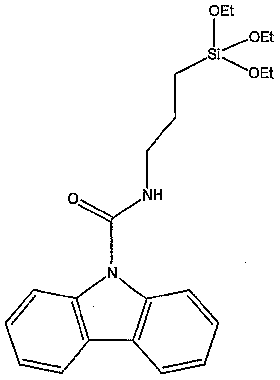
- the preferred precursor preventing the formation of aggregates is a trialkoxysilane comprising a carbazole unit:
- hydrolysis process for hydrolyzable silanes is conventional and known to those skilled in the art.
- Catalysts such as mineral or organic acids can be used.
- an amount of water at least stoichiometric that is to say a molar amount of water corresponding to the number of moles of function capable of generating silanol groups.
- Organic co-solvents such as THF (tetrahydrofuran) can be used.
- a complete hydrolysis is carried out of a mixture of silicon alkoxides, previously dissolved in an organic solvent for the alkoxides, with an acidic aqueous solution of pH equal to 1;
- the acidity of the soil is reduced by partially neutralizing the acid necessary for the hydrolysis by adding a base;
- the soil is then deposited on a substrate by centrifugation technique.
- the film can then be dried at room temperature or subjected to a heat treatment, for example by heating from 50 to 120 ° C, for 5 to 30 minutes.
- the impression of a stable structure is carried out by positioning, by means of an appropriate device, the opening of a fiber tip obtained according to the method described above, in the immediate vicinity of the surface of the layer comprising the photosensitive material, at a distance less than 100 nm, and preferably at a distance less than 50 nm, and better still less than 10 nm.
- a light beam is then injected into the fiber tip and irradiated for a time necessary to obtain the local topographic modification.
- the local topographic modification results directly from the irradiation step and does not require an additional revelation step, as can be seen in certain documents of the prior art.
- the general irradiation conditions are: output power, at the aperture at the tip end: 0.1 to lnW (nano att), the irradiation time varying from 1 to 30 seconds.
- the invention also relates to a method of printing a stable figure represented by raised studs in a layer of a material comprising a photosensitive compound capable of inducing a topographic modification of said layer under the effect of light waves. emitted through at least one opening as defined above, which is characterized in that a) a first pad is printed according to the method described above, b) a controlled lateral movement of said opening is carried out, c) another pad is printed by operating as in step a) above, d) repeating operations b) and c) so as to cover with pads a surface corresponding to said figure.
- the pads obtained have a height of at least 3 nm, preferably from 10 to 50 nm, and a lateral dimension substantially identical to the dimension of the opening and two consecutive pads are distant from less than 200 nm, preferably less than 100 nm, and better still, less than 50 nm.
- a mask consisting of an opaque surface, generally parallel to the surface to be printed, and pierced with one or more openings having the characteristics described above.
- the invention makes it possible to obtain networks of studs whose altitude fluctuation, in the registration area, remains less than their average height, which could not have been obtained in the networks. of the prior art.
- the invention finds applications in the most diverse fields such as the storage of information on discs, fine markings, biotechnology, molecular electronics.
- a particularly interesting application is in the field of ophthalmic lenses.
- microstructure networks of no less than 200 nm, to produce anti-reflective coatings.
- Such a network can be printed directly on the surface of the ophthalmic glass, or on the surface of a mold part and transferred during the molding of the glass.
- Another possible application is the printing of distinctive marks, such as a logo, invisible to the naked eye, and making it possible to identify the origin of the glass.
- An optical fiber is manufactured comprising a terminal portion having the general shape of a point, the end of which has the shape of a truncated cone from a single mode optical fiber marketed by 3M and having the following characteristics:
- - core diameter 3.7 micrometers
- - profile of optical properties between core and cladding index jump type
- This fiber is subjected to a sequential hot stretching following the general process described above with the following parameters
- the optical fiber is held by pinching between two rails, which slide horizontally on ball cages.
- the ends of the rails are connected to each other by a wire which is guided by pulleys and on which hangs a free weight, or any means making it possible to ensure a fixed tension.
- the device includes a laser, the power supply of which is adjusted by a TTL control, as well as a device for measuring the elongation of the fiber.
- a microscope equipped with a camera makes it possible to visualize the fiber during drawing.
- the characteristics of the preformed tip of the fiber obtained after sequential hot stretching are as follows: Diameter of the opening: 477 nm
- a metallization step is then carried out consisting in depositing layers of chromium and aluminum by evaporation under secondary vacuum from metallic filaments heated by Joule effect on the periphery of the fiber tip.
- the first layer is a 10 nm thick bonding layer of chromium deposited over the entire circumference of the tip.
- the chromium is evaporated with a speed of 0.23 nm / s. Still by evaporation, an aluminum layer 100 nm thick is then deposited at an evaporation rate of 1.82 nm / s.
- the tip is kept rotating during the deposition of the layers
- the optical fiber is then ready for use.
- the size of the opening of the fiber tip is of the order of 55 nm. 2 ⁇
- the sample is a thin layer deposited on a glass substrate.
- the layer is obtained by the sol / gel route.
- 2.1 - Preparation of the soil The starting reagents are the following:
- the Si-DRI compound, then the Si-K compound, which is in powder form, are weighed in a pill box.
- the solvent (THF) is then added to the open air, and the solution is homogenized by magnetic stirring.
- the TEOS and the acidified water are added, and the mixture is replaced with magnetic stirring, protected from light for two hours.
- the medium is neutralized by adding 0.0987 cm 3 of pyridine, ie 1.22 x 10 " mole
- the soil is then ready to be deposited (mother solution of concentration denoted C 0 ).
- the deposits are made by centrifugation on glass substrates (microscope slides previously cleaned), for a period of 20 s.
- the condensation process continues, the solvent evaporates, and in the end a thin layer remains, the thickness of which depends on the speed of rotation and the concentration of the soil used.
- the thickness typically varies between 10 nm and approximately 1 ⁇ m; it is determined using a profilometer.
- Adjustment of the thickness of the layer A deposit of the mother solution with a speed of rotation of 3000 revolutions / min makes it possible to obtain a sample of approximately 1 ⁇ m in thickness.
- the mother solution is diluted and the speed of centrifugation is increased.
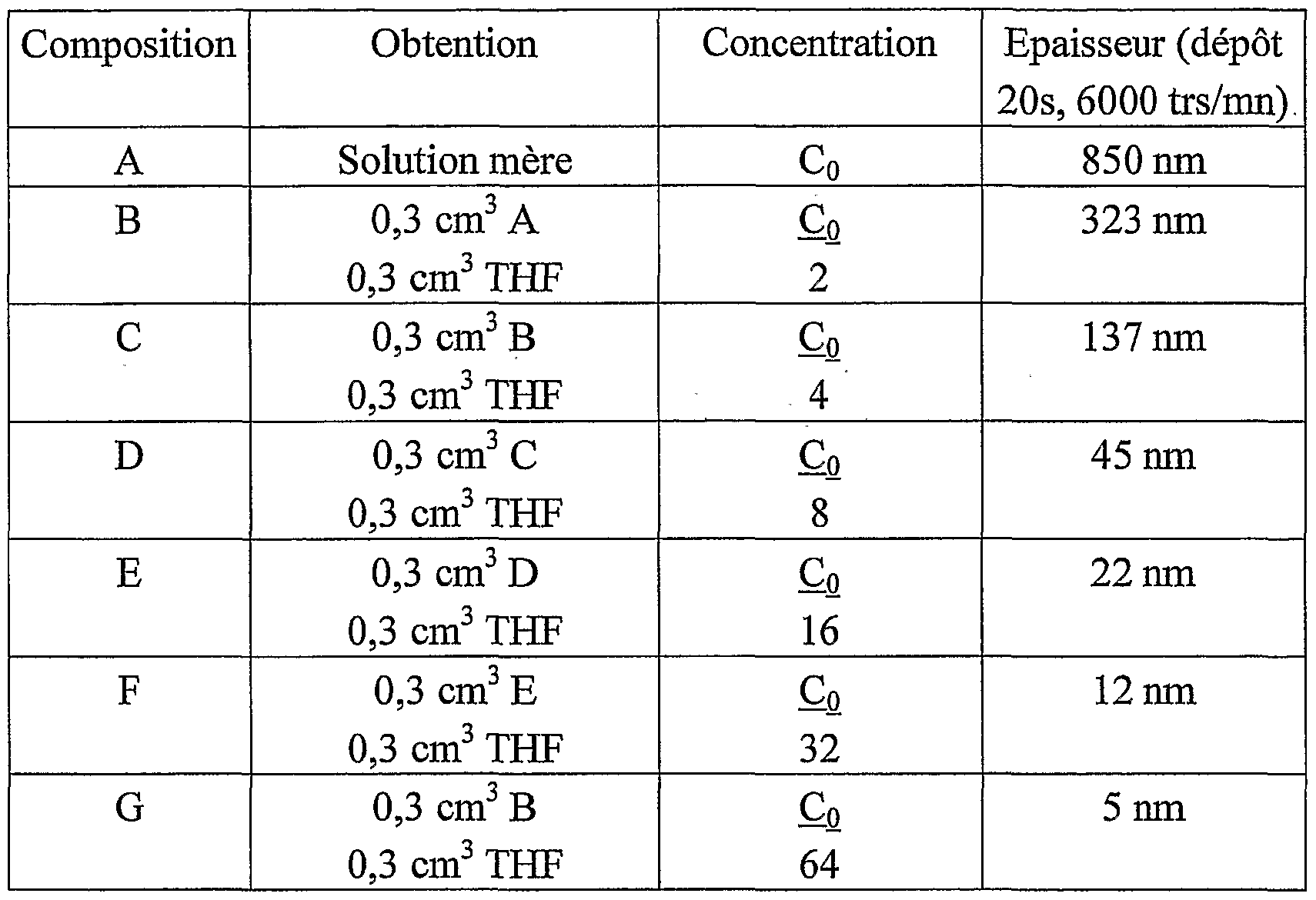
- the table below gives the correspondence between the dilution of the mother solution and the thickness of the sample obtained for a rotation speed fixed at 6000 revolutions / min.
- the thickness measurements are carried out after placing the freshly deposited sample for ten minutes in an oven at 100 ° C. to complete the condensation process and to evaporate the residual solvent.
- An Argon-Krypton laser (1) is used with a wavelength of 568.2 nm (yellow Krypton line) generating a laser beam (3).
- an optical density (2) or neutral filter G4, 2 mm thick is inserted at the output of the laser (1).
- the laser beam (3) crosses the optical density (2) then is reflected by a mirror (4), crosses a quarter-wave plate (5) which transforms the vertical rectilinear polarization coming from the laser (l) into a circular polarization, itself sent to a polarizing filter (6).
- the filter (6) is typically a Polaroid model HN22 polarizer.
- the beam will then be injected into an optical fiber (10), prepared during step 1 above and having one end (11) having a thinned tip and peripherally metallized:
- the beam passes through a connector (9) corresponding to the unmodified end of the optical fiber (10).
- the optical fiber (10) passes through a microscope head (12) containing two piezoelectric tubes, not shown, which make it possible to ensure the displacement, in 3 directions of space, of the end (11) of the optical fiber tip. thinned and peripherally metallized (10).
- a piezoelectric system is described precisely in the thesis of
- the light beam from the opening, not shown, at the end (11) of the fiber tip then passes through the sample (13) prepared during step 2) above. Then the light beam is collected by a microscope objective (14) typically a Zeiss objective, “Epiplan” LD20x / 0.40 and detected by a photomultiplier (16), typically Hamamatsu R943 Ga-As 10 stages, equipped with a polarization analyzer (15). Registration of a network The sample is placed as shown in figure 7 at a distance of
- a first sweep is carried out to check the cleanliness of the surface of the layer on which the network will be written.
- the aperture at the end of the tip is kept at a distance of 5 nm and a scan is carried out in a plane.
- a 2 ⁇ m surface intended to be printed is then checked. Then, by acting on the piezoelectric system, the tip is positioned above a determined point on the swept surface (original position).
- the tip is then moved in two directions x, y perpendicular, in a plane parallel to the surface of the layer, and maintaining the opening at a distance of 5 nm from the surface of the layer.
- a first line of pads is printed by injecting, for two seconds for each pad, a light beam giving a peak output power, at the opening, of 170 pW. Between each light pulse, the point is moved along the x axis by a distance of 116 nm. After the printing of the first line, the point is again placed in its original position and one then carries out a displacement along the axis y of 136 mn, then one prints a new line of pads.
- the operation is repeated until the network is obtained over the entire surface to be printed.
- the studs inscribed have an average height of 5 nm and a half-height width of 55 nm.
- the registered network is shown in Figure 8.
- a network of studs is printed according to the method described in example 1, with a displacement of 200 min from the tip, along the x axis, between each print, and increasing the irradiation time (from 5 to 35 seconds in 5 second steps) for a fixed average output power.
- FIG. 9 represents the sectional view of the network obtained, along one of the lines of the network of studs.
- the height of the pads is directly proportional to the irradiation time.
Landscapes
- Physics & Mathematics (AREA)
- Engineering & Computer Science (AREA)
- General Physics & Mathematics (AREA)
- Nanotechnology (AREA)
- Chemical & Material Sciences (AREA)
- Optics & Photonics (AREA)
- Mathematical Physics (AREA)
- Theoretical Computer Science (AREA)
- Crystallography & Structural Chemistry (AREA)
- Plasma & Fusion (AREA)
- Optical Fibers, Optical Fiber Cores, And Optical Fiber Bundles (AREA)
- Exposure Of Semiconductors, Excluding Electron Or Ion Beam Exposure (AREA)
- Exposure And Positioning Against Photoresist Photosensitive Materials (AREA)
- Printing Plates And Materials Therefor (AREA)
Abstract
Description


Claims
Priority Applications (4)
| Application Number | Priority Date | Filing Date | Title |
|---|---|---|---|
| US10/485,038 US7352384B2 (en) | 2001-07-26 | 2002-07-26 | Method for printing a near field photoinduced stable structure, and optical fibre tip for implementing same |
| EP02772467A EP1415200A1 (fr) | 2001-07-26 | 2002-07-26 | Procede d'impression d'une structure stable photoinduite en champ proche, et pointe de fibre optique pour sa mise en oeuvre |
| JP2003515917A JP4812251B2 (ja) | 2001-07-26 | 2002-07-26 | 光誘導される近距離場の安定構造をプリントする方法、および該方法を実施するための光ファイバチップ |
| US12/026,187 US20080199126A1 (en) | 2001-07-26 | 2008-02-05 | Method for Printing a Near Field Photoinduced Stable Structure, and Optical Fiber Tip for Implementing Same |
Applications Claiming Priority (2)
| Application Number | Priority Date | Filing Date | Title |
|---|---|---|---|
| FR0110019 | 2001-07-26 | ||
| FR0110019A FR2827967B1 (fr) | 2001-07-26 | 2001-07-26 | Procede d'impression d'une structure stable photoinduite en champ proche,et pointe de fibre optique pour sa mise en oeuvre |
Related Child Applications (1)
| Application Number | Title | Priority Date | Filing Date |
|---|---|---|---|
| US12/026,187 Division US20080199126A1 (en) | 2001-07-26 | 2008-02-05 | Method for Printing a Near Field Photoinduced Stable Structure, and Optical Fiber Tip for Implementing Same |
Publications (1)
| Publication Number | Publication Date |
|---|---|
| WO2003010604A1 true WO2003010604A1 (fr) | 2003-02-06 |
Family
ID=8865955
Family Applications (1)
| Application Number | Title | Priority Date | Filing Date |
|---|---|---|---|
| PCT/FR2002/002698 Ceased WO2003010604A1 (fr) | 2001-07-26 | 2002-07-26 | Procede d'impression d'une structure stable photoinduite en champ proche, et pointe de fibre optique pour sa mise en oeuvre |
Country Status (5)
| Country | Link |
|---|---|
| US (2) | US7352384B2 (fr) |
| EP (1) | EP1415200A1 (fr) |
| JP (1) | JP4812251B2 (fr) |
| FR (1) | FR2827967B1 (fr) |
| WO (1) | WO2003010604A1 (fr) |
Citations (5)
| Publication number | Priority date | Publication date | Assignee | Title |
|---|---|---|---|---|
| US4880496A (en) * | 1987-06-30 | 1989-11-14 | Isaiah Nebenzahl | Method and device for submicron precision pattern generation |
| EP0419369A1 (fr) * | 1989-09-22 | 1991-03-27 | Sim (Societe D'investissement Dans La Microscopie) Sa | Procédé de microlithographie en champ proche optique et dispositifs de microlithographie le mettant en oeuvre |
| JPH08248641A (ja) * | 1995-03-13 | 1996-09-27 | Olympus Optical Co Ltd | レーザ描画装置 |
| US5608831A (en) * | 1989-08-08 | 1997-03-04 | E-Tek Dynamics, Inc. | Fiber optic coupler and method of making same |
| EP0880078A2 (fr) * | 1997-05-23 | 1998-11-25 | Canon Kabushiki Kaisha | Dispositif de détection de position, appareil l'utilisant, appareil d'exposition, et méthode de fabrication d'un dispositif l'utilisant |
Family Cites Families (20)
| Publication number | Priority date | Publication date | Assignee | Title |
|---|---|---|---|---|
| US4590492A (en) * | 1983-06-07 | 1986-05-20 | The United States Of America As Represented By The Secretary Of The Air Force | High resolution optical fiber print head |
| US4771415A (en) * | 1985-02-27 | 1988-09-13 | Brother Kogyo Kabushiki Kaisha | Optical data storage and readout apparatus and head, using optical fibers between stationary and movable units |
| US5272330A (en) * | 1990-11-19 | 1993-12-21 | At&T Bell Laboratories | Near field scanning optical microscope having a tapered waveguide |
| CA2054334C (fr) * | 1990-11-19 | 1995-11-28 | Robert Eric Betzig | Microscope optique a balayage en champ proche et applications de ce microscope |
| US5288997A (en) * | 1990-11-19 | 1994-02-22 | At&T Bell Laboratories | Manufacturing method, including near-field optical microscopic examination of a magnetic bit pattern |
| US5729331A (en) * | 1993-06-30 | 1998-03-17 | Nikon Corporation | Exposure apparatus, optical projection apparatus and a method for adjusting the optical projection apparatus |
| US5531343A (en) * | 1993-07-15 | 1996-07-02 | At&T Corp. | Cylindrical fiber probe devices and methods of making them |
| JPH07106229A (ja) * | 1993-10-05 | 1995-04-21 | Hitachi Ltd | 光リソグラフィ方法及び装置 |
| US5394500A (en) * | 1993-12-22 | 1995-02-28 | At&T Corp. | Fiber probe device having multiple diameters |
| JP3264824B2 (ja) * | 1996-04-11 | 2002-03-11 | セイコーインスツルメンツ株式会社 | 光伝搬体プローブと走査型近視野顕微鏡及び光伝搬体プローブの透過孔形成方法 |
| US5932397A (en) * | 1996-05-28 | 1999-08-03 | Rvm Scientific, Inc. | Multicolor lithography for control of three dimensional refractive index gradient processing |
| US6236783B1 (en) * | 1996-09-06 | 2001-05-22 | Kanagawa Academy Of Science And Technology | Optical fiber probe and manufacturing method therefor |
| JP3363787B2 (ja) * | 1998-05-02 | 2003-01-08 | キヤノン株式会社 | 露光方法および露光装置 |
| JP3901867B2 (ja) * | 1999-02-08 | 2007-04-04 | 富士フイルム株式会社 | 近接場光記録再生装置 |
| JP2001062574A (ja) * | 1999-06-25 | 2001-03-13 | Kanagawa Acad Of Sci & Technol | 微細加工装置 |
| JP4395942B2 (ja) * | 1999-11-12 | 2010-01-13 | 株式会社豊田中央研究所 | 光記録方法及び試料観察方法 |
| JP4992026B2 (ja) * | 2000-12-27 | 2012-08-08 | 独立行政法人産業技術総合研究所 | 近接場光評価方法 |
| US6899999B2 (en) * | 2001-03-28 | 2005-05-31 | Kabushiki Kaisha Toshiba | Method of manufacturing composite member, photosensitive composition, porous base material, insulating body and composite member |
| JP2002296169A (ja) * | 2001-03-30 | 2002-10-09 | Canon Inc | 近接場光プローブ、及び該近接場光プローブを有する近接場光学顕微鏡、近接場光リソグラフィー装置、近接場光ストレージ装置 |
| DE10303961B4 (de) * | 2003-01-31 | 2005-03-24 | Fraunhofer-Gesellschaft zur Förderung der angewandten Forschung e.V. | Sonde für ein optisches Nahfeldmikroskop und Verfahren zu deren Herstellung |
-
2001
- 2001-07-26 FR FR0110019A patent/FR2827967B1/fr not_active Expired - Lifetime
-
2002
- 2002-07-26 WO PCT/FR2002/002698 patent/WO2003010604A1/fr not_active Ceased
- 2002-07-26 EP EP02772467A patent/EP1415200A1/fr not_active Ceased
- 2002-07-26 JP JP2003515917A patent/JP4812251B2/ja not_active Expired - Lifetime
- 2002-07-26 US US10/485,038 patent/US7352384B2/en not_active Expired - Lifetime
-
2008
- 2008-02-05 US US12/026,187 patent/US20080199126A1/en not_active Abandoned
Patent Citations (5)
| Publication number | Priority date | Publication date | Assignee | Title |
|---|---|---|---|---|
| US4880496A (en) * | 1987-06-30 | 1989-11-14 | Isaiah Nebenzahl | Method and device for submicron precision pattern generation |
| US5608831A (en) * | 1989-08-08 | 1997-03-04 | E-Tek Dynamics, Inc. | Fiber optic coupler and method of making same |
| EP0419369A1 (fr) * | 1989-09-22 | 1991-03-27 | Sim (Societe D'investissement Dans La Microscopie) Sa | Procédé de microlithographie en champ proche optique et dispositifs de microlithographie le mettant en oeuvre |
| JPH08248641A (ja) * | 1995-03-13 | 1996-09-27 | Olympus Optical Co Ltd | レーザ描画装置 |
| EP0880078A2 (fr) * | 1997-05-23 | 1998-11-25 | Canon Kabushiki Kaisha | Dispositif de détection de position, appareil l'utilisant, appareil d'exposition, et méthode de fabrication d'un dispositif l'utilisant |
Non-Patent Citations (2)
| Title |
|---|
| PATENT ABSTRACTS OF JAPAN vol. 1997, no. 01 31 January 1997 (1997-01-31) * |
| See also references of EP1415200A1 * |
Also Published As
| Publication number | Publication date |
|---|---|
| JP2004536465A (ja) | 2004-12-02 |
| EP1415200A1 (fr) | 2004-05-06 |
| JP4812251B2 (ja) | 2011-11-09 |
| FR2827967A1 (fr) | 2003-01-31 |
| US7352384B2 (en) | 2008-04-01 |
| FR2827967B1 (fr) | 2003-10-24 |
| US20040214115A1 (en) | 2004-10-28 |
| US20080199126A1 (en) | 2008-08-21 |
Similar Documents
| Publication | Publication Date | Title |
|---|---|---|
| Houbertz et al. | Inorganic–organic hybrid polymers for information technology: from planar technology to 3D nanostructures | |
| EP0061378B1 (fr) | Procédé de modification contrôlée des caractéristiques géométriques de l'extrémité d'une fibre optique monomode, et application au couplage optique | |
| EP3924757B1 (fr) | Métasurfaces optiques, procédés et systèmes de fabrication associés | |
| FR2774998A1 (fr) | Materiau photochromique a variation stable d'indice de refraction et/ou de birefringence | |
| James et al. | Surface engineering of polystyrene–cerium oxide nanocomposite thin films for refractive index enhancement | |
| EP3475742B1 (fr) | Procédés et systèmes de fonctionnalisation optique d'un échantillon en matériau semi-conducteur | |
| WO2019186070A1 (fr) | Procédé pour la réalisation d'un objet tridimensionnel par un processus de photopolymérisation multi-photonique et dispositif associé | |
| Kuleshova et al. | Automated device for vertical deposition of colloidal opal films | |
| EP2616235A1 (fr) | Procédé de fabrication d'une structure optique segmentée | |
| WO2009144187A1 (fr) | Dispositif de piégeage de particules | |
| WO2003010604A1 (fr) | Procede d'impression d'une structure stable photoinduite en champ proche, et pointe de fibre optique pour sa mise en oeuvre | |
| JP5343479B2 (ja) | 二光子吸収有機材料とその用途 | |
| Agnarsson et al. | Low-temperature fabrication and characterization of a symmetric hybrid organic–inorganic slab waveguide for evanescent light microscopy | |
| WO2009141436A1 (fr) | Ensemble micro-optique | |
| FR2936321A1 (fr) | Revetements anti-reflet comprenant des objets disperses presentant deux domaines separes ayant des indices de refraction distincts. | |
| WO2016184770A1 (fr) | Fibre optique ruban en verre photosensible | |
| EP2396642A1 (fr) | Systeme et equipement de detection optique de particules a eventail de decouplage de l'information optique, procede de fabrication correspondant | |
| WO2014016514A1 (fr) | Procédé de fabrication d'une couche mince solide minérale transparente et biréfringente et composant optique à couche mince solide minérale transparente et biréfringente | |
| WO2017178209A1 (fr) | Procede et appareil de positionnement d'un micro- ou nano-objet sous controle visuel | |
| EP4406006B1 (fr) | Procédé de fabrication d'un moule pour nano-impression et moule associé | |
| WO2006003313A1 (fr) | Procede de fabrication d’un bloc optique a circuit optique integre par photopolymerisation localisee d’une matrice organique par absorption a deux photons et bloc optique ainsi obtenu | |
| Zhang et al. | Laboratory for Nano-photonic Structures and Integrated Devices on Fiber End Facets | |
| FR3097326A1 (fr) | Dispositif et procédé d'observation d'un échantillon fluorescent | |
| EP3655821A1 (fr) | Procédé de lithographie interférentielle | |
| Leitel et al. | Stochastic subwavelength structures on poly (methyl methacrylate) surfaces for antireflection generated by plasma treatment |
Legal Events
| Date | Code | Title | Description |
|---|---|---|---|
| AK | Designated states |
Kind code of ref document: A1 Designated state(s): AE AG AL AM AT AU AZ BA BB BG BR BY BZ CA CH CN CO CR CU CZ DE DK DM DZ EC EE ES FI GB GD GE GH GM HR HU ID IL IN IS JP KE KG KP KR KZ LC LK LR LS LT LU LV MA MD MG MK MN MW MX MZ NO NZ OM PH PL PT RO RU SD SE SG SI SK SL TJ TM TN TR TT TZ UA UG US UZ VN YU ZA ZM ZW Kind code of ref document: A1 Designated state(s): AE AG AL AM AT AU AZ BA BB BG BY BZ CA CH CN CO CR CU CZ DE DM DZ EC EE ES FI GB GD GE GH HR HU ID IL IN IS JP KE KG KP KR LC LK LR LS LT LU LV MA MD MG MN MW MX MZ NO NZ OM PH PL PT RU SD SE SG SI SK SL TJ TM TN TR TZ UA UG US UZ VN YU ZA ZM |
|
| AL | Designated countries for regional patents |
Kind code of ref document: A1 Designated state(s): GH GM KE LS MW MZ SD SL SZ TZ UG ZM ZW AM AZ BY KG KZ MD RU TJ TM AT BE BG CH CY CZ DE DK EE ES FI FR GB GR IE IT LU MC NL PT SE SK TR BF BJ CF CG CI CM GA GN GQ GW ML MR NE SN TD TG Kind code of ref document: A1 Designated state(s): GH GM KE LS MW MZ SD SL SZ UG ZM ZW AM AZ BY KG KZ RU TJ TM AT BE BG CH CY CZ DK EE ES FI FR GB GR IE IT LU MC PT SE SK TR BF BJ CF CG CI GA GN GQ GW ML MR NE SN TD TG US |
|
| 121 | Ep: the epo has been informed by wipo that ep was designated in this application | ||
| WWE | Wipo information: entry into national phase |
Ref document number: 2002772467 Country of ref document: EP |
|
| WWE | Wipo information: entry into national phase |
Ref document number: 10485038 Country of ref document: US Ref document number: 2003515917 Country of ref document: JP |
|
| WWP | Wipo information: published in national office |
Ref document number: 2002772467 Country of ref document: EP |
|
| REG | Reference to national code |
Ref country code: DE Ref legal event code: 8642 |