WO2005010479A2 - Procede de mesure de parametres physiques d'au moins une phase aux dimensions micrometriques ou nanometriques dans un systeme composite. - Google Patents
Procede de mesure de parametres physiques d'au moins une phase aux dimensions micrometriques ou nanometriques dans un systeme composite. Download PDFInfo
- Publication number
- WO2005010479A2 WO2005010479A2 PCT/FR2004/001877 FR2004001877W WO2005010479A2 WO 2005010479 A2 WO2005010479 A2 WO 2005010479A2 FR 2004001877 W FR2004001877 W FR 2004001877W WO 2005010479 A2 WO2005010479 A2 WO 2005010479A2
- Authority
- WO
- WIPO (PCT)
- Prior art keywords
- phase
- sample
- interface
- substrate
- layer
- Prior art date
- Legal status (The legal status is an assumption and is not a legal conclusion. Google has not performed a legal analysis and makes no representation as to the accuracy of the status listed.)
- Ceased
Links
Classifications
-
- G—PHYSICS
- G01—MEASURING; TESTING
- G01F—MEASURING VOLUME, VOLUME FLOW, MASS FLOW OR LIQUID LEVEL; METERING BY VOLUME
- G01F1/00—Measuring the volume flow or mass flow of fluid or fluent solid material wherein the fluid passes through a meter in a continuous flow
- G01F1/68—Measuring the volume flow or mass flow of fluid or fluent solid material wherein the fluid passes through a meter in a continuous flow by using thermal effects
- G01F1/684—Structural arrangements; Mounting of elements, e.g. in relation to fluid flow
-
- H—ELECTRICITY
- H01—ELECTRIC ELEMENTS
- H01J—ELECTRIC DISCHARGE TUBES OR DISCHARGE LAMPS
- H01J37/00—Discharge tubes with provision for introducing objects or material to be exposed to the discharge, e.g. for the purpose of examination or processing thereof
- H01J37/26—Electron or ion microscopes; Electron or ion diffraction tubes
- H01J37/295—Electron or ion diffraction tubes
- H01J37/2955—Electron or ion diffraction tubes using scanning ray
-
- G—PHYSICS
- G01—MEASURING; TESTING
- G01N—INVESTIGATING OR ANALYSING MATERIALS BY DETERMINING THEIR CHEMICAL OR PHYSICAL PROPERTIES
- G01N21/00—Investigating or analysing materials by the use of optical means, i.e. using sub-millimetre waves, infrared, visible or ultraviolet light
-
- G—PHYSICS
- G01—MEASURING; TESTING
- G01N—INVESTIGATING OR ANALYSING MATERIALS BY DETERMINING THEIR CHEMICAL OR PHYSICAL PROPERTIES
- G01N23/00—Investigating or analysing materials by the use of wave or particle radiation, e.g. X-rays or neutrons, not covered by groups G01N3/00 – G01N17/00, G01N21/00 or G01N22/00
- G01N23/22—Investigating or analysing materials by the use of wave or particle radiation, e.g. X-rays or neutrons, not covered by groups G01N3/00 – G01N17/00, G01N21/00 or G01N22/00 by measuring secondary emission from the material
- G01N23/225—Investigating or analysing materials by the use of wave or particle radiation, e.g. X-rays or neutrons, not covered by groups G01N3/00 – G01N17/00, G01N21/00 or G01N22/00 by measuring secondary emission from the material using electron or ion
- G01N23/2251—Investigating or analysing materials by the use of wave or particle radiation, e.g. X-rays or neutrons, not covered by groups G01N3/00 – G01N17/00, G01N21/00 or G01N22/00 by measuring secondary emission from the material using electron or ion using incident electron beams, e.g. scanning electron microscopy [SEM]
-
- B—PERFORMING OPERATIONS; TRANSPORTING
- B82—NANOTECHNOLOGY
- B82Y—SPECIFIC USES OR APPLICATIONS OF NANOSTRUCTURES; MEASUREMENT OR ANALYSIS OF NANOSTRUCTURES; MANUFACTURE OR TREATMENT OF NANOSTRUCTURES
- B82Y35/00—Methods or apparatus for measurement or analysis of nanostructures
Definitions
- the subject of the present invention is a method for determining at least one mechanical parameter of at least one material in a composite system comprising at least two distinct phases.
- the method applies more particularly to the case where the phase to be characterized is structured on a micrometric or nanometric scale, and at least one other material constitutes a substrate or a matrix.
- the method applies to the characterization of a thin layer deposited on a substrate or of inclusions, filaments or fibers in a matrix.
- mechanical parameters is used here to indicate both mechanical and thermomechanical properties, such as Young's modulus, Poisson's ratio, coefficient of thermal expansion, etc., as well as deformation and / or de constraint.
- Knowledge of the mechanical properties of a physical system or device makes it possible to optimize its operation. Any material whatsoever is subject to external stresses and it must be possible to know its resistance to such stresses. It is therefore important to know as well as possible the elastic properties of a system and in particular those of one or more layers placed on the surface of a substrate. The properties of this layer (or of these layers considered as a subsystem) differ significantly from the properties of the layers taken individually.
- the elastic properties of materials are involved in many fields of application: coating of mechanical parts, structural deformation, etc.
- Electroacoustic waves for example Hardness and Young's modulus of high-quality cubic boron nitride films grown by chemical vapor deposition.
- the object of the invention is to measure one or more mechanical parameters, in particular the elastic constants and the coefficients of thermal expansion of a material and the stresses that this material generates when it is associated with others. Its specificity is to be able to measure such parameters under conditions close to their application condition: thin or thick layers, layers inhomogeneous, discontinuous or precipitated 'layers' / inclusions, fibers or filaments, boxes (term more specific to semiconductor materials where the charges are located in these boxes made of a second material different from the substrate).
- strain parameter is meant both the pure strains, commonly indicated by the symbol ⁇ and which, from a microscopic point of view, correspond to variations in the crystalline parameters, as well as the local rotations of the crystal axes, indicated by the symbol ⁇ .
- the invention therefore relates to a method for determining at least one mechanical parameter of at least one material in a composite system comprising at least two distinct phases, characterized in that it comprises: (a) carrying out at least one sample comprising a first part of a first phase and a second part of a second phase, the second part consisting of the material to be characterized, the sample having at least a dimension sufficiently small to allow a relaxation of the stresses in said sample; (b) measuring, on said sample at least one deformation parameter of at least said first phase, in correspondence with a plurality of points located at different distances from an interface between said first and second phase; and (c) determining, from at least said deformation parameter, at least one mechanical parameter of said second phase.
- Said method comprises: i.
- Step b. is repeated at at least two different temperatures for at least one of said samples.
- Step c. includes: i. modeling the relaxation of stresses in said sample (L) using a first estimate of at least one mechanical property of the material of said second phase (B); ii. comparing the results of the measurements in step b. with those of said modeling; iii. the modification of said estimate of at least one mechanical property of the material of said second phase and the reiteration of sub-steps i. to iii.
- Said composite system is chosen from: a substrate having on its surface a continuous layer, a substrate having on its surface islands or metallization strips, a layer with an area included in the substrate, a transistor, a layer inside of a substrate, a matrix containing inclusions, fibers or filaments.
- Said sample comprises at least one dimension on the micrometric or nanometric scale.
- Said sample is a blade having two substantially parallel faces and arranged substantially perpendicular to the interface between said first and second phases, in which case step b. is advantageously repeated for a plurality of blades of different thicknesses.
- said sample is a slide arranged at an angle relative to the interface between said first and second phases, in which case step b. is advantageously repeated for a plurality of blades arranged at different angles relative to the interface between said first and second phases.
- said sample is a wedge-shaped blade, having two faces forming an angle between them, in which case step b. is advantageously repeated for a plurality of blades having two faces forming between them different angles - -
- the measures provided for in step b. are made by diffraction of a convergent electron beam. Step b.
- Step b. involves determining at least the width of at least some of said Holz lines and calculating, for each of them, a maximum rotation ⁇ ma ⁇ along the axis of the electron beam.
- Step c. implements the layout of at least one curve representing a said maximum rotation as a function of the distance from the interface between said first and second phases. According to a preferred embodiment, step c.
- a tungsten contact constitutes the drain contact D.
- the analyzed area ( Figure 2b) is pointed by the arrow F.
- the thin blade shown in Figure 2b has a thickness t (which can be varied).
- the average incident electron beam for the "CBED" shots (direction z 0 ) is taken along the y 2 axis which makes an angle ⁇ with the y axis ! normal to the blade.
- the directions and the corresponding crystallographic axes are illustrated in FIG. 2b.
- CBED is the acronym for "convergent beam electron diffraction", Convergent Beam
- FIG. 3 a is a montage of photos illustrating five of the "CBED" diffraction diagrams chosen from around fifty images actually produced, along a straight line perpendicular to the surface (direction - z), at a distance of 155 nm from contact D of drain.
- the curve in Figure 3b representing the evolution of the angle ⁇ calculated as a function of -z.
- Figure 4b is the snapshot 4a on which lines of
- the first line system represents the simulation of the diffraction pattern of a perfect silicon crystal disoriented by + ⁇ ma ⁇ relative to the axis x 2 // [3-20] ;
- the second line system represents the simulation of the diffraction pattern of a disoriented perfect silicon crystal by - ⁇ max with respect to the x 2 axis // [3-20];
- the third line system (in dotted lines ) represents the simulation of the diffraction pattern of the non-disoriented perfect crystal.
- ⁇ the angle 2 ⁇ max. .
- Figures 6a to 6d illustrate the feasibility of minimizing the elasticity coefficients of the material.
- Figure 7b is a profile which was produced on the Holz strip
- FIG. 7c is a simulation of the profile of FIG. 7b which shows that it is possible to reproduce the widening of the Holz lines and the variations of intensity 1 - A ⁇ ( ⁇ ) in the Holz bands.
- This simulation used the results of the finite element calculation which is an illustration of point iv (constants optimized elastic and displacement R (y 1 , z 1 )).
- the widths ⁇ g of axis x // were taken into account [320].
- FIGS. 8 to 8d illustrate a second experimental example, in which the silicon substrate A is surmounted by a layer of Si ( i- X) Ge x , then by a layer of Si on the surface.
- Figure 8a shows the thin blade of thickness t.
- FIGS. 8b to 8d are diffraction patterns "CBED" respectively in the direction [230] inside the layer Si (1. X) Ge x , in the substrate Si far from the deformed zone, and in the substrate So close to the deformed area.
- FIG. 9 shows a flowchart of an embodiment of the method of the invention.
- the method of the invention comprises: a) producing a blade L of thickness t sufficiently small and having two substantially parallel faces and arranged substantially perpendicular to said substrate surface; b) measuring on said plate at least one parameter for deformation of the substrate at different depths relative to the surface; by deformation parameter, we also mean the substrate rotation parameter; c) determining from at least said deformation / rotation parameter at least one mechanical parameter of said layer.
- the method may include the production of several blades of different thicknesses as well as the implementation of step b on each of said blades.
- step b can be repeated at at least two different temperatures.
- Said measurement is advantageously carried out by generating, for points of the substrate situated at different depths, diffraction diagrams of a convergent electron beam (CBED) of axis Z 0 disoriented with respect to the normal to said plate, said diagrams comprising Holz lines or bands.
- the determination ç can then include the recording of the width of the Holz lines of at least some of said diagrams, for at least one crystallographic plane of the substrate. From the width of these Holz lines, we can calculate for each diagram a maximum rotation ⁇ max along the axis of the electron beam.
- This rotation is induced by the layer (or layers) placed on the substrate and it characterizes its properties.
- a similar technique could be used in the case of anisotropic modeling with the coefficients known to those skilled in the art.
- point (i) The thin blade with controlled geometry is extracted or thinned in the device. A parallel face blade is preferable but not essential. A slight angle may be present.
- We used a focused ion beam 'FIB' but alternative methods, conventional in preparation of samples for electron microscopy can be used (mechanical thinning, cleavage, ...) but the technique 'FIB' has the advantage of being fast and not to mechanically disturb the system or device and to fully control the operations.
- CBED convergent electron beam
- part b is composed of a homogeneous layer of a given material
- the measurements need not be carried out on the same blade successively thinned to different thicknesses.
- Working on a single blade increases precision and is essential in the case where the system consists of a single nanosystem (transistor for example).
- a single blade thickness does not allow to correctly calculate all the constants of the material.
- a single blade thickness gives information only on the material constraints (this is the case of the study of the curvature of semiconductor wafers or 'wafers' via the Stoney formula). The constraints are partly relaxed by a curvature of the substrate (see for example: Measurement of elastic modulus, Poisson ratio, and coefficient of thermal expansion of on-wafer submicron films.
- the invention will find many applications in the surface treatment of mechanical parts, optimization of electronic circuits (contact metal, oxide layer, etc.) or devices where the presence of two different materials necessarily creates mechanical stresses.
- the method according to the invention is original although it uses well known techniques or physical effects: - the technique of the focused ion beam or 'FIB' (Focus Ion
- Deliverable D23 uses a similar technique ('FIB', convergent beam, simulation), but the technique essentially measures variations in crystalline parameters while the method according to the invention is mainly concerned with local rotations of the crystal lattice.
- the STREAM project does not seek to measure elastic constants, but to measure constrained deformations in integrated circuits.
- the STREAM project measured only variations in crystalline parameters far from the two parts A and B of the device and neglected stress relaxation in the thin section.
- the detection of rotation of the crystal lattice according to the invention makes it possible to be faster, more precise and to approach the interface between parts A and B.
- the power of the method according to the invention has been shown by analyzing the deformations introduced by a layer of NiSi in an integrated circuit
- the relationships between the microscope mark and the crystal mark depend on the orientation of the sample in the microscope.
- CBED diagrams are taken every 4 nm in a direction perpendicular to the surface (direction z 2 ), starting from the surface, but only ten are retained in the calculations.
- Figure 3 shows the position along the z axis where 5 of these experimental shots were obtained.
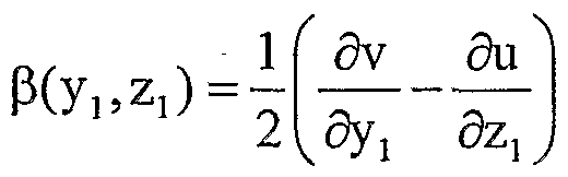
- a rotation of axis X] and of angle ⁇ (y ls z_) can be broken down into 3 rotations of axis x 2 , of angle ⁇ (yi, z), of axis y 2 , of angle ⁇ ' (y 1; zi) and z, of angle ⁇ "(y ⁇ , z_).
- ⁇ (y ⁇ , Z!> 0.98 ⁇ (y h z_)
- OC B and ⁇ T have been optimized by minimizing the distance ⁇ between the experimental and calculated curves (see Figure 6)) using the distortion hypothesis planar.
- the strains are calculated in the plane defined by the direction of the incident electrons yi // zO and the axis z ⁇ .
- State 3 Before extraction of the blade, the system was much more constrained because the stresses are not released by the surfaces. Once the parameters (for example the elasticity coefficient and the thermal expansion coefficient) have been evaluated, it is possible, by the present process, to evaluate the stresses in the integrated circuit before thinning.
- the stresses in the transistor are calculated using the optimized constants: these are the stresses taken in the middle of a very thick plate t 0 or those of a periodic blade of infinite thickness.
- Step E1 of the process is the cutting of at least one blade comprising a part of the substrate and a part of the layer disposed on its surface. This results in a relaxation of the stresses (E2), and therefore a deformation of said blade.
- at least one deformation parameter (preferably a rotation ⁇ ) is measured in correspondence with a plurality of points of the blade, at different depths relative to the layer-substrate interface.
- step E4 modeling is carried out, typically by finite elements, of the constrained blade, that is to say before its cutting.
- a first estimate is made of the mechanical properties of the thin layer, such as its Young's modulus E ', its Poisson's ratio v' and its coherence temperature T'o (step E4).
- step E5 the stress relaxation is modeled. This can be done by replacing conditions with the imposed displacement contour (zero) by free contour conditions.
- step E6 on the basis of this simulation, the expected values ⁇ ', ⁇ ' of the deformation parameter or parameters are determined in correspondence of the points where the measurements of the step E3 have been carried out.
- steps E1 - E6 are repeated for a plurality of blades of different thicknesses, or more generally having a different geometry, and / or at different temperatures.
- the mean square error between the measured and expected values is calculated (E7), and minimized by variation of the estimates of the mechanical properties of the thin layer (E9) and iteration of steps E4 - E7, until convergence is reached (E8). In this way, an optimal estimate is obtained, in the sense of the mean square error, of the mechanical properties of said layer (E10).
- the information thus obtained is used, in step El i, to calculate a state of deformation and / or stress of the thin layer and / or of the substrate.
- the different measurements of deformation parameters were carried out at different depths compared to the layer-substrate interface. More generally, in the case of inclusions, fibers or filaments, it will not be possible to speak of "depth", but simply of the distance from the interface between the two phases considered.
- some of the measurement points may, at least in certain cases, be located inside the nanometric or micrometric phase to be characterized.
- CEBD can be used, such as LACBED (Large Angle Convergent Beam Electron Diffraction: diffraction of a convergent beam of electrons at large angle).
- LACBED Large Angle Convergent Beam Electron Diffraction: diffraction of a convergent beam of electrons at large angle.
- the only deformation parameter considered was the angle of rotation ⁇ , determined by measuring the enlargement ⁇ of the Holz lines.
- the displacement of the Holz lines, linked to pure deformations, could also have been taken into account.
- the method of the invention may include the use of one or more deformation parameters, determined from different quantities measured directly.
Landscapes
- Chemical & Material Sciences (AREA)
- Analytical Chemistry (AREA)
- Physics & Mathematics (AREA)
- General Physics & Mathematics (AREA)
- General Health & Medical Sciences (AREA)
- Biochemistry (AREA)
- Life Sciences & Earth Sciences (AREA)
- Health & Medical Sciences (AREA)
- Immunology (AREA)
- Pathology (AREA)
- Fluid Mechanics (AREA)
- Analysing Materials By The Use Of Radiation (AREA)
- Investigating Strength Of Materials By Application Of Mechanical Stress (AREA)
- Recrystallisation Techniques (AREA)
Abstract
Description


Claims
Priority Applications (4)
| Application Number | Priority Date | Filing Date | Title |
|---|---|---|---|
| US10/565,034 US20060288797A1 (en) | 2003-07-18 | 2004-07-16 | Method for measuring physical parameters of at least one micrometric or nanometric dimensional phase in a composite system |
| EP04767701A EP1649269A2 (fr) | 2003-07-18 | 2004-07-16 | Procede de mesure de parametres physiques d au moins une phase aux dimensions micrometriques ou nanometriques dans un systeme composite. |
| CA002532471A CA2532471A1 (fr) | 2003-07-18 | 2004-07-16 | Procede de mesure de parametres physiques d'au moins une phase aux dimensions micrometriques ou nanometriques dans un systeme composite |
| JP2006519968A JP2007528998A (ja) | 2003-07-18 | 2004-07-16 | 複合系における少なくとも一つのマイクロメートル又はナノメートル寸法の相の物理パラメータを計測する方法 |
Applications Claiming Priority (2)
| Application Number | Priority Date | Filing Date | Title |
|---|---|---|---|
| FR0308782A FR2857751B1 (fr) | 2003-07-18 | 2003-07-18 | Procede de mesure de parametres physiques d'au moins une couche d'un materiau aux dimensions micrometriques |
| FR0308782 | 2003-07-18 |
Publications (2)
| Publication Number | Publication Date |
|---|---|
| WO2005010479A2 true WO2005010479A2 (fr) | 2005-02-03 |
| WO2005010479A3 WO2005010479A3 (fr) | 2005-06-09 |
Family
ID=33548242
Family Applications (1)
| Application Number | Title | Priority Date | Filing Date |
|---|---|---|---|
| PCT/FR2004/001877 Ceased WO2005010479A2 (fr) | 2003-07-18 | 2004-07-16 | Procede de mesure de parametres physiques d'au moins une phase aux dimensions micrometriques ou nanometriques dans un systeme composite. |
Country Status (8)
| Country | Link |
|---|---|
| US (1) | US20060288797A1 (fr) |
| EP (1) | EP1649269A2 (fr) |
| JP (1) | JP2007528998A (fr) |
| KR (1) | KR20060059963A (fr) |
| CN (1) | CN1826523A (fr) |
| CA (1) | CA2532471A1 (fr) |
| FR (1) | FR2857751B1 (fr) |
| WO (1) | WO2005010479A2 (fr) |
Families Citing this family (5)
| Publication number | Priority date | Publication date | Assignee | Title |
|---|---|---|---|---|
| JP4640811B2 (ja) * | 2005-09-28 | 2011-03-02 | 富士通株式会社 | 応力測定方法及び装置 |
| JPWO2011108468A1 (ja) * | 2010-03-02 | 2013-06-27 | 日本電気株式会社 | 材料定数推定システム及び材料定数推定方法 |
| US9625823B1 (en) * | 2010-06-17 | 2017-04-18 | Kla-Tencor Corporation | Calculation method for local film stress measurements using local film thickness values |
| ITRM20120017A1 (it) * | 2012-01-18 | 2013-07-19 | Univ Degli Studi Roma Tre | Metodo per la misura del rapporto di poisson e dello stress residuo |
| CN104833574B (zh) * | 2015-05-14 | 2017-08-25 | 云南师范大学 | 一种单缝衍射实验测量装置 |
Family Cites Families (2)
| Publication number | Priority date | Publication date | Assignee | Title |
|---|---|---|---|---|
| US5221367A (en) * | 1988-08-03 | 1993-06-22 | International Business Machines, Corp. | Strained defect-free epitaxial mismatched heterostructures and method of fabrication |
| US7430920B2 (en) * | 2005-12-16 | 2008-10-07 | Hitachi, Ltd. | Apparatus for measuring a mechanical quantity |
-
2003
- 2003-07-18 FR FR0308782A patent/FR2857751B1/fr not_active Expired - Fee Related
-
2004
- 2004-07-16 KR KR1020067001205A patent/KR20060059963A/ko not_active Withdrawn
- 2004-07-16 EP EP04767701A patent/EP1649269A2/fr not_active Withdrawn
- 2004-07-16 JP JP2006519968A patent/JP2007528998A/ja not_active Withdrawn
- 2004-07-16 WO PCT/FR2004/001877 patent/WO2005010479A2/fr not_active Ceased
- 2004-07-16 CN CNA2004800207266A patent/CN1826523A/zh active Pending
- 2004-07-16 US US10/565,034 patent/US20060288797A1/en not_active Abandoned
- 2004-07-16 CA CA002532471A patent/CA2532471A1/fr not_active Abandoned
Non-Patent Citations (6)
| Title |
|---|
| ARMIGLIATO A ET AL: "APPLICATION OF CONVERGENT BEAM ELECTRON DIFFRACTION TO TWO-DIMENSIONAL STRAIN MAPING IN SILICON DEVICES" APPLIED PHYSICS LETTERS, AMERICAN INSTITUTE OF PHYSICS. NEW YORK, US, vol. 82, no. 13, 31 mars 2003 (2003-03-31), pages 2172-2174, XP001166504 ISSN: 0003-6951 * |
| CLEMENT L ET AL: "Strain measurements by convergent-beam electron diffraction: the importance of stress relaxation in lamella preparations" APPLIED PHYSICS LETTERS AIP USA, vol. 85, no. 4, 26 juillet 2004 (2004-07-26), pages 651-653, XP002316655 ISSN: 0003-6951 * |
| GAMBETTA F ET AL: "Large angle convergent beam electron diffraction strain measurements in high dose helium implanted silicon" MATERIALS SCIENCE AND ENGINEERING B, ELSEVIER SEQUOIA, LAUSANNE, CH, vol. 71, no. 1-3, février 2000 (2000-02), pages 87-91, XP004185754 ISSN: 0921-5107 * |
| LI B ET AL: "A Study of Residual Strain in a K2O.6TiO2W/Al Composite by Using Convergent Beam Electron Diffraction" SCRIPTA MATERIALIA, ELSEVIER, NEW YORK, NY, US, vol. 38, no. 9, 3 avril 1998 (1998-04-03), pages 1419-1425, XP004325156 ISSN: 1359-6462 * |
| PAILLOUX F ET AL: "Stress relaxation in c[perpendicular]-c//YBaCuO thin films on MgO substrate studied by LACBED" THIN SOLID FILMS ELSEVIER SWITZERLAND, vol. 368, no. 1, 1 juin 2000 (2000-06-01), pages 142-146, XP004203950 ISSN: 0040-6090 * |
| WAKAYAMA Y ET AL: "STRAIN DISTRIBUTION NEAR SI/NISI2 INTERFACE MEASURED BY CONVERGENT BEAM ELECTRON DIFFRACTION" JAPANESE JOURNAL OF APPLIED PHYSICS, PUBLICATION OFFICE JAPANESE JOURNAL OF APPLIED PHYSICS. TOKYO, JP, vol. 35, PART 2, no. 12B, 15 décembre 1996 (1996-12-15), pages L1662-L1665, XP000735155 ISSN: 0021-4922 * |
Also Published As
| Publication number | Publication date |
|---|---|
| CA2532471A1 (fr) | 2005-02-03 |
| WO2005010479A3 (fr) | 2005-06-09 |
| CN1826523A (zh) | 2006-08-30 |
| EP1649269A2 (fr) | 2006-04-26 |
| FR2857751A1 (fr) | 2005-01-21 |
| FR2857751B1 (fr) | 2005-12-30 |
| JP2007528998A (ja) | 2007-10-18 |
| KR20060059963A (ko) | 2006-06-02 |
| US20060288797A1 (en) | 2006-12-28 |
Similar Documents
| Publication | Publication Date | Title |
|---|---|---|
| Hruszkewycz et al. | Quantitative nanoscale imaging of lattice distortions in epitaxial semiconductor heterostructures using nanofocused X-ray Bragg projection ptychography | |
| Xu et al. | Generalized phase-shifting interferometry with arbitrary unknown phase shifts: Direct wave-front reconstruction by blind phase shift extraction and its experimental verification | |
| EP2880426B1 (fr) | Procédé d'analyse de la structure cristalline d'un matériau semi-conducteur poly-cristallin | |
| Dushaq et al. | Hexagonal germanium formation at room temperature using controlled penetration depth nano-indentation | |
| Sabaté et al. | Measurement of residual stresses in micromachined structures in a microregion | |
| Nieborek et al. | Optimization of the plasmonic properties of titanium nitride films sputtered at room temperature through microstructure and thickness control | |
| Gailhanou et al. | Strain field in silicon on insulator lines using high resolution x-ray diffraction | |
| Teplin et al. | Monitoring and modeling silicon homoepitaxy breakdown with real-time spectroscopic ellipsometry | |
| Hofmann et al. | THz dielectric anisotropy of metal slanted columnar thin films | |
| EP1649269A2 (fr) | Procede de mesure de parametres physiques d au moins une phase aux dimensions micrometriques ou nanometriques dans un systeme composite. | |
| Okudur et al. | Extraction of elastic modulus of porous ultra-thin low-k films by two-dimensional finite-element simulations of nanoindentation | |
| Jiang et al. | Grain boundary effects on the optical constants and Drude relaxation times of silver films | |
| Kalaswad et al. | Sputter-deposited Mo Thin films: multimodal characterization of structure, surface morphology, density, residual stress, electrical resistivity, and mechanical response | |
| Faurie et al. | Determination of elastic constants of a fiber-textured gold film by combining synchrotron x-ray diffraction and in situ tensile testing | |
| Schmidt et al. | In-line Raman spectroscopy for gate-all-around nanosheet device manufacturing | |
| Kim et al. | High-throughput analysis of thin-film stresses using arrays of micromachined cantilever beams | |
| Lin et al. | Scalar scattering model of highly textured transparent conducting oxide | |
| Useinov et al. | Optical spectroscopy combined in situ with instrumented indentation | |
| Akagawa et al. | High-precision characterization of textured a-Si: H/SnO2: F structures by spectroscopic ellipsometry | |
| Diebold | Nanoscale characterization and metrology | |
| Murray et al. | Nanoscale silicon-on-insulator deformation induced by stressed liner structures | |
| Stevens et al. | Amorphous silicon layer characteristics during 70–2000eV Ar+-ion bombardment of Si (100) | |
| Treger et al. | Characterization of room temperature recrystallization kinetics in electroplated copper thin films with concurrent x-ray diffraction and electrical resistivity measurements | |
| Zushi et al. | Phonon Dispersion in< 100> Si Nanowire Covered with SiO2 Film Calculated by Molecular Dynamics Simulation | |
| Niebelschütz et al. | Work function analysis of GaN-based lateral polarity structures by Auger electron energy measurements |
Legal Events
| Date | Code | Title | Description |
|---|---|---|---|
| WWE | Wipo information: entry into national phase |
Ref document number: 200480020726.6 Country of ref document: CN |
|
| AK | Designated states |
Kind code of ref document: A2 Designated state(s): AE AG AL AM AT AU AZ BA BB BG BR BW BY BZ CA CH CN CO CR CU CZ DE DK DM DZ EC EE EG ES FI GB GD GE GH GM HR HU ID IL IN IS JP KE KG KP KR KZ LC LK LR LS LT LU LV MA MD MG MK MN MW MX MZ NA NI NO NZ OM PG PH PL PT RO RU SC SD SE SG SK SL SY TJ TM TN TR TT TZ UA UG US UZ VC VN YU ZA ZM ZW |
|
| AL | Designated countries for regional patents |
Kind code of ref document: A2 Designated state(s): BW GH GM KE LS MW MZ NA SD SL SZ TZ UG ZM ZW AM AZ BY KG KZ MD RU TJ TM AT BE BG CH CY CZ DE DK EE ES FI FR GB GR HU IE IT LU MC NL PL PT RO SE SI SK TR BF BJ CF CG CI CM GA GN GQ GW ML MR NE SN TD TG |
|
| 121 | Ep: the epo has been informed by wipo that ep was designated in this application | ||
| ENP | Entry into the national phase |
Ref document number: 2532471 Country of ref document: CA |
|
| WWE | Wipo information: entry into national phase |
Ref document number: 2006519968 Country of ref document: JP |
|
| WWE | Wipo information: entry into national phase |
Ref document number: 1020067001205 Country of ref document: KR |
|
| WWE | Wipo information: entry into national phase |
Ref document number: 256/KOLNP/2006 Country of ref document: IN |
|
| WWE | Wipo information: entry into national phase |
Ref document number: 2004767701 Country of ref document: EP |
|
| WWP | Wipo information: published in national office |
Ref document number: 2004767701 Country of ref document: EP |
|
| WWP | Wipo information: published in national office |
Ref document number: 1020067001205 Country of ref document: KR |
|
| WWE | Wipo information: entry into national phase |
Ref document number: 2006288797 Country of ref document: US Ref document number: 10565034 Country of ref document: US |
|
| WWP | Wipo information: published in national office |
Ref document number: 10565034 Country of ref document: US |