WO2006095539A1 - 有機電界発光素子及びその製造 - Google Patents
有機電界発光素子及びその製造 Download PDFInfo
- Publication number
- WO2006095539A1 WO2006095539A1 PCT/JP2006/302502 JP2006302502W WO2006095539A1 WO 2006095539 A1 WO2006095539 A1 WO 2006095539A1 JP 2006302502 W JP2006302502 W JP 2006302502W WO 2006095539 A1 WO2006095539 A1 WO 2006095539A1
- Authority
- WO
- WIPO (PCT)
- Prior art keywords
- group
- organic
- organic electroluminescent
- layer
- ring
- Prior art date
- Legal status (The legal status is an assumption and is not a legal conclusion. Google has not performed a legal analysis and makes no representation as to the accuracy of the status listed.)
- Ceased
Links
Classifications
-
- H—ELECTRICITY
- H05—ELECTRIC TECHNIQUES NOT OTHERWISE PROVIDED FOR
- H05B—ELECTRIC HEATING; ELECTRIC LIGHT SOURCES NOT OTHERWISE PROVIDED FOR; CIRCUIT ARRANGEMENTS FOR ELECTRIC LIGHT SOURCES, IN GENERAL
- H05B33/00—Electroluminescent light sources
- H05B33/12—Light sources with substantially two-dimensional [2D] radiating surfaces
- H05B33/14—Light sources with substantially two-dimensional [2D] radiating surfaces characterised by the chemical or physical composition or the arrangement of the electroluminescent material, or by the simultaneous addition of the electroluminescent material in or onto the light source
-
- C—CHEMISTRY; METALLURGY
- C09—DYES; PAINTS; POLISHES; NATURAL RESINS; ADHESIVES; COMPOSITIONS NOT OTHERWISE PROVIDED FOR; APPLICATIONS OF MATERIALS NOT OTHERWISE PROVIDED FOR
- C09K—MATERIALS FOR MISCELLANEOUS APPLICATIONS, NOT PROVIDED FOR ELSEWHERE
- C09K11/00—Luminescent materials, e.g. electroluminescent or chemiluminescent
- C09K11/02—Use of particular materials as binders, particle coatings or suspension media therefor
- C09K11/025—Use of particular materials as binders, particle coatings or suspension media therefor non-luminescent particle coatings or suspension media
-
- C—CHEMISTRY; METALLURGY
- C09—DYES; PAINTS; POLISHES; NATURAL RESINS; ADHESIVES; COMPOSITIONS NOT OTHERWISE PROVIDED FOR; APPLICATIONS OF MATERIALS NOT OTHERWISE PROVIDED FOR
- C09K—MATERIALS FOR MISCELLANEOUS APPLICATIONS, NOT PROVIDED FOR ELSEWHERE
- C09K11/00—Luminescent materials, e.g. electroluminescent or chemiluminescent
- C09K11/06—Luminescent materials, e.g. electroluminescent or chemiluminescent containing organic luminescent materials
-
- H—ELECTRICITY
- H10—SEMICONDUCTOR DEVICES; ELECTRIC SOLID-STATE DEVICES NOT OTHERWISE PROVIDED FOR
- H10K—ORGANIC ELECTRIC SOLID-STATE DEVICES
- H10K50/00—Organic light-emitting devices
-
- H—ELECTRICITY
- H10—SEMICONDUCTOR DEVICES; ELECTRIC SOLID-STATE DEVICES NOT OTHERWISE PROVIDED FOR
- H10K—ORGANIC ELECTRIC SOLID-STATE DEVICES
- H10K50/00—Organic light-emitting devices
- H10K50/10—OLEDs or polymer light-emitting diodes [PLED]
- H10K50/11—OLEDs or polymer light-emitting diodes [PLED] characterised by the electroluminescent [EL] layers
-
- H—ELECTRICITY
- H10—SEMICONDUCTOR DEVICES; ELECTRIC SOLID-STATE DEVICES NOT OTHERWISE PROVIDED FOR
- H10K—ORGANIC ELECTRIC SOLID-STATE DEVICES
- H10K50/00—Organic light-emitting devices
- H10K50/10—OLEDs or polymer light-emitting diodes [PLED]
- H10K50/14—Carrier transporting layers
-
- H—ELECTRICITY
- H10—SEMICONDUCTOR DEVICES; ELECTRIC SOLID-STATE DEVICES NOT OTHERWISE PROVIDED FOR
- H10K—ORGANIC ELECTRIC SOLID-STATE DEVICES
- H10K85/00—Organic materials used in the body or electrodes of devices covered by this subclass
- H10K85/10—Organic polymers or oligomers
- H10K85/111—Organic polymers or oligomers comprising aromatic, heteroaromatic, or aryl chains, e.g. polyaniline, polyphenylene or polyphenylene vinylene
-
- H—ELECTRICITY
- H10—SEMICONDUCTOR DEVICES; ELECTRIC SOLID-STATE DEVICES NOT OTHERWISE PROVIDED FOR
- H10K—ORGANIC ELECTRIC SOLID-STATE DEVICES
- H10K85/00—Organic materials used in the body or electrodes of devices covered by this subclass
- H10K85/30—Coordination compounds
- H10K85/321—Metal complexes comprising a group IIIA element, e.g. Tris (8-hydroxyquinoline) gallium [Gaq3]
- H10K85/322—Metal complexes comprising a group IIIA element, e.g. Tris (8-hydroxyquinoline) gallium [Gaq3] comprising boron
-
- H—ELECTRICITY
- H10—SEMICONDUCTOR DEVICES; ELECTRIC SOLID-STATE DEVICES NOT OTHERWISE PROVIDED FOR
- H10K—ORGANIC ELECTRIC SOLID-STATE DEVICES
- H10K85/00—Organic materials used in the body or electrodes of devices covered by this subclass
- H10K85/30—Coordination compounds
- H10K85/321—Metal complexes comprising a group IIIA element, e.g. Tris (8-hydroxyquinoline) gallium [Gaq3]
- H10K85/324—Metal complexes comprising a group IIIA element, e.g. Tris (8-hydroxyquinoline) gallium [Gaq3] comprising aluminium, e.g. Alq3
-
- H—ELECTRICITY
- H10—SEMICONDUCTOR DEVICES; ELECTRIC SOLID-STATE DEVICES NOT OTHERWISE PROVIDED FOR
- H10K—ORGANIC ELECTRIC SOLID-STATE DEVICES
- H10K85/00—Organic materials used in the body or electrodes of devices covered by this subclass
- H10K85/30—Coordination compounds
- H10K85/341—Transition metal complexes, e.g. Ru(II)polypyridine complexes
- H10K85/342—Transition metal complexes, e.g. Ru(II)polypyridine complexes comprising iridium
-
- H—ELECTRICITY
- H10—SEMICONDUCTOR DEVICES; ELECTRIC SOLID-STATE DEVICES NOT OTHERWISE PROVIDED FOR
- H10K—ORGANIC ELECTRIC SOLID-STATE DEVICES
- H10K85/00—Organic materials used in the body or electrodes of devices covered by this subclass
- H10K85/60—Organic compounds having low molecular weight
-
- H—ELECTRICITY
- H10—SEMICONDUCTOR DEVICES; ELECTRIC SOLID-STATE DEVICES NOT OTHERWISE PROVIDED FOR
- H10K—ORGANIC ELECTRIC SOLID-STATE DEVICES
- H10K85/00—Organic materials used in the body or electrodes of devices covered by this subclass
- H10K85/60—Organic compounds having low molecular weight
- H10K85/615—Polycyclic condensed aromatic hydrocarbons, e.g. anthracene
-
- H—ELECTRICITY
- H10—SEMICONDUCTOR DEVICES; ELECTRIC SOLID-STATE DEVICES NOT OTHERWISE PROVIDED FOR
- H10K—ORGANIC ELECTRIC SOLID-STATE DEVICES
- H10K85/00—Organic materials used in the body or electrodes of devices covered by this subclass
- H10K85/60—Organic compounds having low molecular weight
- H10K85/615—Polycyclic condensed aromatic hydrocarbons, e.g. anthracene
- H10K85/626—Polycyclic condensed aromatic hydrocarbons, e.g. anthracene containing more than one polycyclic condensed aromatic rings, e.g. bis-anthracene
-
- H—ELECTRICITY
- H10—SEMICONDUCTOR DEVICES; ELECTRIC SOLID-STATE DEVICES NOT OTHERWISE PROVIDED FOR
- H10K—ORGANIC ELECTRIC SOLID-STATE DEVICES
- H10K85/00—Organic materials used in the body or electrodes of devices covered by this subclass
- H10K85/60—Organic compounds having low molecular weight
- H10K85/631—Amine compounds having at least two aryl rest on at least one amine-nitrogen atom, e.g. triphenylamine
-
- H—ELECTRICITY
- H10—SEMICONDUCTOR DEVICES; ELECTRIC SOLID-STATE DEVICES NOT OTHERWISE PROVIDED FOR
- H10K—ORGANIC ELECTRIC SOLID-STATE DEVICES
- H10K85/00—Organic materials used in the body or electrodes of devices covered by this subclass
- H10K85/60—Organic compounds having low molecular weight
- H10K85/631—Amine compounds having at least two aryl rest on at least one amine-nitrogen atom, e.g. triphenylamine
- H10K85/636—Amine compounds having at least two aryl rest on at least one amine-nitrogen atom, e.g. triphenylamine comprising heteroaromatic hydrocarbons as substituents on the nitrogen atom
-
- H—ELECTRICITY
- H10—SEMICONDUCTOR DEVICES; ELECTRIC SOLID-STATE DEVICES NOT OTHERWISE PROVIDED FOR
- H10K—ORGANIC ELECTRIC SOLID-STATE DEVICES
- H10K85/00—Organic materials used in the body or electrodes of devices covered by this subclass
- H10K85/60—Organic compounds having low molecular weight
- H10K85/649—Aromatic compounds comprising a hetero atom
- H10K85/654—Aromatic compounds comprising a hetero atom comprising only nitrogen as heteroatom
-
- H—ELECTRICITY
- H10—SEMICONDUCTOR DEVICES; ELECTRIC SOLID-STATE DEVICES NOT OTHERWISE PROVIDED FOR
- H10K—ORGANIC ELECTRIC SOLID-STATE DEVICES
- H10K85/00—Organic materials used in the body or electrodes of devices covered by this subclass
- H10K85/60—Organic compounds having low molecular weight
- H10K85/649—Aromatic compounds comprising a hetero atom
- H10K85/657—Polycyclic condensed heteroaromatic hydrocarbons
- H10K85/6572—Polycyclic condensed heteroaromatic hydrocarbons comprising only nitrogen in the heteroaromatic polycondensed ring system, e.g. phenanthroline or carbazole
-
- C—CHEMISTRY; METALLURGY
- C09—DYES; PAINTS; POLISHES; NATURAL RESINS; ADHESIVES; COMPOSITIONS NOT OTHERWISE PROVIDED FOR; APPLICATIONS OF MATERIALS NOT OTHERWISE PROVIDED FOR
- C09K—MATERIALS FOR MISCELLANEOUS APPLICATIONS, NOT PROVIDED FOR ELSEWHERE
- C09K2211/00—Chemical nature of organic luminescent or tenebrescent compounds
- C09K2211/10—Non-macromolecular compounds
- C09K2211/1003—Carbocyclic compounds
- C09K2211/1007—Non-condensed systems
-
- C—CHEMISTRY; METALLURGY
- C09—DYES; PAINTS; POLISHES; NATURAL RESINS; ADHESIVES; COMPOSITIONS NOT OTHERWISE PROVIDED FOR; APPLICATIONS OF MATERIALS NOT OTHERWISE PROVIDED FOR
- C09K—MATERIALS FOR MISCELLANEOUS APPLICATIONS, NOT PROVIDED FOR ELSEWHERE
- C09K2211/00—Chemical nature of organic luminescent or tenebrescent compounds
- C09K2211/10—Non-macromolecular compounds
- C09K2211/1018—Heterocyclic compounds
- C09K2211/1025—Heterocyclic compounds characterised by ligands
- C09K2211/1029—Heterocyclic compounds characterised by ligands containing one nitrogen atom as the heteroatom
-
- C—CHEMISTRY; METALLURGY
- C09—DYES; PAINTS; POLISHES; NATURAL RESINS; ADHESIVES; COMPOSITIONS NOT OTHERWISE PROVIDED FOR; APPLICATIONS OF MATERIALS NOT OTHERWISE PROVIDED FOR
- C09K—MATERIALS FOR MISCELLANEOUS APPLICATIONS, NOT PROVIDED FOR ELSEWHERE
- C09K2211/00—Chemical nature of organic luminescent or tenebrescent compounds
- C09K2211/18—Metal complexes
- C09K2211/185—Metal complexes of the platinum group, i.e. Os, Ir, Pt, Ru, Rh or Pd
-
- H—ELECTRICITY
- H10—SEMICONDUCTOR DEVICES; ELECTRIC SOLID-STATE DEVICES NOT OTHERWISE PROVIDED FOR
- H10K—ORGANIC ELECTRIC SOLID-STATE DEVICES
- H10K2101/00—Properties of the organic materials covered by group H10K85/00
- H10K2101/10—Triplet emission
-
- H—ELECTRICITY
- H10—SEMICONDUCTOR DEVICES; ELECTRIC SOLID-STATE DEVICES NOT OTHERWISE PROVIDED FOR
- H10K—ORGANIC ELECTRIC SOLID-STATE DEVICES
- H10K50/00—Organic light-emitting devices
- H10K50/10—OLEDs or polymer light-emitting diodes [PLED]
- H10K50/14—Carrier transporting layers
- H10K50/16—Electron transporting layers
-
- H—ELECTRICITY
- H10—SEMICONDUCTOR DEVICES; ELECTRIC SOLID-STATE DEVICES NOT OTHERWISE PROVIDED FOR
- H10K—ORGANIC ELECTRIC SOLID-STATE DEVICES
- H10K50/00—Organic light-emitting devices
- H10K50/10—OLEDs or polymer light-emitting diodes [PLED]
- H10K50/17—Carrier injection layers
-
- H—ELECTRICITY
- H10—SEMICONDUCTOR DEVICES; ELECTRIC SOLID-STATE DEVICES NOT OTHERWISE PROVIDED FOR
- H10K—ORGANIC ELECTRIC SOLID-STATE DEVICES
- H10K50/00—Organic light-emitting devices
- H10K50/10—OLEDs or polymer light-emitting diodes [PLED]
- H10K50/18—Carrier blocking layers
-
- H—ELECTRICITY
- H10—SEMICONDUCTOR DEVICES; ELECTRIC SOLID-STATE DEVICES NOT OTHERWISE PROVIDED FOR
- H10K—ORGANIC ELECTRIC SOLID-STATE DEVICES
- H10K71/00—Manufacture or treatment specially adapted for the organic devices covered by this subclass
- H10K71/10—Deposition of organic active material
- H10K71/12—Deposition of organic active material using liquid deposition, e.g. spin coating
- H10K71/15—Deposition of organic active material using liquid deposition, e.g. spin coating characterised by the solvent used
Definitions
- the present invention provides a composition for an organic electroluminescence device capable of easily producing an organic electroluminescence device excellent in luminous efficiency and driving life by a wet film-forming method, and using the composition for an organic electroluminescence device.
- BACKGROUND OF THE INVENTION 1 Field of the Invention The present invention relates to a thin film for an organic electroluminescent element, a member for transferring a thin film for an organic electroluminescent element, an organic electroluminescent element, and a method for producing the organic electroluminescent element.
- organic electroluminescent element using an organic thin film.
- the materials for organic electroluminescence devices can be classified mainly into low-molecular materials and high-molecular materials.
- an organic electroluminescent device provided with a hole transport layer having an aromatic diamine power and a light-emitting layer having an aluminum complex power of 8-hydroxyquinoline, or a coumarin using an aluminum complex of 8-hydroxyquinoline as a host material
- Organic electroluminescent devices using low molecular weight materials such as organic electroluminescent devices doped with laser fluorescent dyes such as these have been developed.
- low molecular weight materials such as the following platinum complexes and iridium complexes are also used as materials for the light emitting layer.
- poly (p-phenylene-lenylene), poly [2-methoxy-5- (2-ethylhexyloxy) -1,4-phenylene-lenylene], poly (3-alkylthiophene) Development of organic electroluminescent devices using polymer materials such as high molecular weight materials, and devices in which polymer materials such as polyvinyl carbazole are mixed with low molecular light emitting materials and electron transfer materials are also underway.
- the element fabrication process using these polymer materials is mostly a wet film forming method such as spin coating or an ink jet method because of the characteristics of the material.
- the vacuum deposition method has advantages such as being able to form a high-quality film uniformly on the substrate, easy to obtain a device with excellent characteristics and easy lamination, and very little contamination from the manufacturing process.
- the majority of organic electroluminescent devices currently in practical use are produced by vacuum evaporation using low molecular weight materials.
- the wet film-forming method does not require a vacuum process and is easy in a large area, and a single layer (coating liquid) can contain a plurality of materials having various functions.
- a single layer coating liquid
- the wet film-forming method has the following problems, and the present situation is that it will reach a practical level except for elements using some polymer materials. It is difficult to control the degree of polymerization and molecular weight distribution of polymer materials (polymerized organic compounds).
- Patent Document 1 and Patent Document 2 listed below are low-level materials composed of a fluorescent material, a hole transport material, and an electron transport material, which are not the same as a polymer material (polymerized organic compound).
- the use of molecular materials (non-polymerizable organic compounds) is described. This is an attempt to lower the driving voltage by transporting holes injected from the anode and electrons injected from the cathode by the hole transport material and the electron transport material, respectively.
- these devices were insufficient in hole injection and electron injection from the anode and cathode, so that the driving voltage was high and the light emission efficiency was insufficient.
- the oxadiazole derivative used as an electron transport material has a problem in driving stability, and the driving life is not sufficient. Furthermore, when trying to apply phosphorescent materials or blue light emitting materials to the light emitting material, the energy gap of the light emitting material is large, making it difficult to apply.
- Patent Document 1 Japanese Patent No. 3069139
- Patent Document 2 Japanese Patent Laid-Open No. 11-273859
- the present invention is an organic electroluminescent device in which an organic light emitting layer is formed by a wet film forming method.
- An object of the present invention is to provide an organic electroluminescence device having good charge injection characteristics from an electrode to an organic light emitting layer, and excellent in luminous efficiency and driving life.
- the composition for an organic electroluminescent element of the first aspect of the present invention contains a phosphorescent material, a charge transport material, and a solvent.
- a phosphorescent material a charge transport material
- a solvent a solvent that is a non-polymerized organic compound.
- the thin film for organic electroluminescent elements of the second aspect is formed by a wet film forming method using the composition for organic electroluminescent elements of the first aspect.
- the thin film transfer member for an organic electroluminescence device according to the third aspect is formed on a substrate by a wet film forming method using the composition for an organic electroluminescence device of the first aspect.
- the organic electroluminescence device of the fourth aspect has an anode, a cathode, and an organic light emitting layer provided between both electrodes, and the organic light emitting layer is used for thin film transfer for the organic electroluminescence device of the third aspect. It is a layer formed using a member.
- the organic electroluminescent device of the fifth aspect has an anode, a cathode, and an organic light emitting layer provided between both electrodes, and the organic light emitting layer is a composition for an organic electroluminescent device outside the first space. Is a layer formed by a wet film-forming method.
- a sixth method for producing an organic electroluminescent device is a method for producing an organic electroluminescent device having an anode, a cathode, and an organic luminescent layer provided between both electrodes on a substrate.
- FIG. 1 is a schematic cross-sectional view showing an example of a thin film transfer member for an organic electroluminescent element.
- FIG. 2 is a schematic cross-sectional view showing an example of an organic electroluminescent element.
- FIG. 3 is a schematic cross-sectional view showing another example of an organic electroluminescent element.
- FIG. 4 is a schematic cross-sectional view showing another example of an organic electroluminescent element.
- FIG. 5 is a schematic cross-sectional view showing another example of an organic electroluminescent element.
- FIG. 6 is a schematic cross-sectional view showing another example of an organic electroluminescent element.
- FIG. 7 is a schematic cross-sectional view showing another example of an organic electroluminescent element.
- FIG. 8 is a graph showing an electroluminescence spectrum of the device produced in Example 1.
- the composition for organic electroluminescent elements of the present invention has a long pot life, excellent thermal stability, low viscosity, excellent uniformity, and easy film thickness adjustment during film formation.
- an organic electroluminescent device having good charge injection characteristics from the electrode to the organic luminescent layer and excellent in luminous efficiency and driving life can be easily obtained by a wet film forming method. be able to.
- the phosphorescent light emitting material and the charge transport material are greatly involved in the injection of either holes or electrons, and as a result, the driving voltage is lowered.
- the LUMO of the phosphorescent light emitting material increases or decreases, and the charge from the LUMO or HOMO of the charge transporting material is reduced. Light emission from the phosphorescent material can be obtained with high efficiency because the level is easy to receive.
- a thin film for an organic electroluminescent element of the present invention formed by a wet film-forming method using the composition for an organic electroluminescent element of the present invention has excellent luminescent properties, excellent film quality, and excellent thermal stability. ⁇ It is hard to deteriorate even if it is energized for a long time.
- the thin film transfer member for an organic electroluminescent element of the present invention formed on a substrate by a wet film-forming method using the composition for an organic electroluminescent element of the present invention, the light emitting property is excellent.
- An organic thin film with good film quality, excellent thermal stability, and hardly deteriorated even when energized for a long time can be easily formed.
- the organic electroluminescence device of the present invention forms an organic light emitting layer by a wet film forming method using the composition for organic electroluminescence device of the present invention.
- the element can be easily manufactured by a simple process.
- the organic electroluminescent device of the present invention is a flat panel display (for example, a wall-mounted TV for OA computer), an in-vehicle display device, a mobile phone display, or a light source that produces features as a surface light emitter (for example, a copy).
- a flat panel display for example, a wall-mounted TV for OA computer
- an in-vehicle display device for example, a mobile phone display
- a light source that produces features as a surface light emitter (for example, a copy).
- composition for an organic electroluminescent device of the present invention contains a phosphorescent material, a charge transport material and a solvent,
- Each of the phosphorescent light emitting material and the charge transport material is a non-polymerized organic compound.
- the definitions of the non-polymerization type organic compound, the phosphorescent light emitting material, and the charge transport material are as follows.
- This non-polymerizable organic compound refers to a compound other than a compound generally called a polymer (polymerized organic compound). That is, it refers to a substance other than a substance composed of a high molecular weight polymer or a condensate molecule produced by repeating the same reaction or a similar reaction in a chain. Specifically, it is different from so-called high molecular weight organic compounds prepared by polymerizing a single or plural polymerizable monomers, oligomers or polymers regularly or irregularly by any method. It refers to a compound having a substantially single molecular weight, and is a compound whose molecular structure can be uniquely and quantitatively defined by a chemical formula.
- This phosphorescent material refers to a component that mainly emits light in the organic electroluminescent device of the present invention, and corresponds to a dopant component in the organic electroluminescent device.
- the amount of light emitted from the organic electroluminescent element usually 10 to 100%, preferably 20 to 100%, more preferably 50 to 100%, most preferably 80 to 100% When identified as luminescence from a material, it is defined as a luminescent material.
- the phosphorescent material may have charge transporting properties as long as the light emitting function is not impaired.
- the phosphorescent material may be a single compound or a combination of two or more compounds in any combination and ratio.
- the “phosphorescent material” may be simply referred to as “luminescent material”.
- This charge transport material is a material that can transfer a given charge (that is, electrons and holes), and any material that does not have any other restrictions can be used as long as the above conditions are satisfied. it can. Also, the charge transport material may be a single compound or a combination of two or more compounds in any combination and ratio.
- the first oxidation potential and the first reduction potential can be measured by the electrochemical measurement (cyclic voltammetry) described below.
- the supporting electrolyte, the solvent, and the electrode used for the measurement are not limited to the examples shown below, and any one can be used as long as the same level of measurement is possible.
- a measurement target material (according to the present invention) is added to an organic solvent containing about 0.1 mol / L of tetraptyl ammonium perchlorate or tetrabutyl ammonium hexafluorophosphate. (Light emitting material or charge transport material) is dissolved in an amount of about 0.1 to 2 mM.
- a glassy carbon electrode for example, is used as the working electrode, and platinum, for example, is used as the counter electrode.
- the value obtained by converting the thus obtained acid (or reduction) potential further using the saturated sweet potato electrode (SCE) as a reference electrode is the first acid (or reduction) potential in the present invention.
- the organic solvent used for the measurement should be one having a sufficiently reduced water content, such as acetonitrile, methylene chloride, N, N-dimethylformamide, or tetrahydrofuran.
- the light emitting material or charge transporting material according to the invention is well dissolved, and it is difficult for itself to be electrolytically oxidized (or reduced), so that a potential window can be widened.
- any known material can be used as the phosphorescent material, and the phosphorescent materials can be used alone or in combination.
- the phosphorescent material is excellent from the viewpoint of internal quantum efficiency.
- a fluorescent light emitting material is used instead of the phosphorescent light emitting material, even if the relationship between the charge transport material and the light emitting material is satisfied, the effect of improving the efficiency or the life cannot be obtained.
- the phosphorescent material preferably includes, for example, an organometallic complex containing a metal selected from Groups 7 to 11 of the periodic table (IUP AC Periodic Table of the Elements, 2004).
- Preferred examples of the metal in the phosphorescent organometallic complex containing a metal selected from Group 11 of the Periodic Table 7 include ruthenium, rhodium, palladium, silver, rhenium, osmium, iridium, platinum, and gold.
- Preferred examples of these organometallic complexes include compounds represented by the following formulas (4) and (5), and compounds described in WO2005 / 011370 and WO2005 / 019373.
- M represents a metal
- q represents the valence of the metal M
- G and G ′ represent a bidentate ligand.
- j represents 0, 1 or 2;
- M 5 represents a metal
- T represents carbon or nitrogen.
- R 92 to R 95 each independently represent a substituent. However, when T is nitrogen, R 94 and R There is no 95. )
- M represents any metal, and specific examples of preferable ones include those in the periodic table 7 to Group 11 power The metal mentioned above is mentioned as a metal selected.
- bidentate ligands G and G ′ in the formula (4) each represent a ligand having the following partial structure.
- G ′ is particularly preferably from the viewpoint of the stability of the complex
- the ring Q1 represents an aromatic hydrocarbon group or an aromatic heterocyclic group, and these may have a substituent.
- Ring Q2 represents a nitrogen-containing aromatic heterocyclic group, which may have a substituent.
- “may have a substituent” means that it may have one or more substituents.
- Preferred substituents for the rings Ql and Q2 include halogen atoms such as fluorine atoms; alkyl groups such as methyl groups and ethyl groups; alkenyl groups such as bur groups; methoxycarbo yl groups and ethoxy carbo- groups.
- Alkoxy group such as ruthenium group; alkoxy group such as methoxy group and ethoxy group
- An aryloxy group such as a phenoxy group or a benzyloxy group; a dialkylamino group such as a dimethylamino group or a jetamino group; a diarylamino group such as a diphenylamino group; a carbazolyl group; an acyl group such as a acetyl group; a trifluoromethyl group; A haloalkyl group; a cyano group; an aromatic hydrocarbon group such as a full group, a naphthyl group, and a phenanthyl group.
- the compound represented by the formula (4) is more preferably a compound represented by the following formula (4a), (4b), (4c).
- M a represents the same metal as M, and q represents the valence of the metal M a .
- Ring Q1 represents an aromatic hydrocarbon group or aromatic heterocyclic group which may have a substituent, and ring Q2 has a substituent! /, May be a nitrogen-containing aromatic heterocyclic group Represents.
- M b represents the same metal as M, and q b represents the valence of the metal M b .
- Ring Q1 represents an aromatic hydrocarbon group or aromatic heterocyclic group which may have a substituent, and ring Q2 has a substituent! /, May be a nitrogen-containing aromatic heterocyclic group Represents.
- M e represents the same metal as M, q e represents the valence of the metal M e.
- j represents 0, 1 or 2;
- Ring Q1 and ring Q1 ′ each independently represent an aromatic hydrocarbon group or an aromatic heterocyclic group which may have a substituent.
- Ring Q2 and ring Q2 ′ each independently have a substituent! / May represent a nitrogen-containing aromatic heterocyclic group.
- the ring Q1 and the ring Q1 ' are preferably, for example, a phenyl group, a biphenyl group, a naphthyl group, an anthryl group, a chelate group, Group, furyl group, benzochelyl group, benzofuryl group, pyridyl group, quinolyl group, isoquinolyl group, carbazolyl group and the like.
- ring Q2 and ring Q2 ′ for example, pyridyl group, pyrimidyl group, pyrazyl group, triazyl group, benzothiazole group, benzoxazole group, benzimidazole group, quinolyl group, isoquinolyl group, quinoxalyl group are preferable.
- phenanthridyl group for example, pyridyl group, pyrimidyl group, pyrazyl group, triazyl group, benzothiazole group, benzoxazole group, benzimidazole group, quinolyl group, isoquinolyl group, quinoxalyl group are preferable.
- phenanthridyl group for example, pyridyl group, pyrimidyl group, pyrazyl group, triazyl group, benzothiazole group, benzoxazole group, benzimidazole group, quinolyl group, isoquinolyl group, quinox
- the substituents that the compounds represented by the formulas (4a), (4b), and (4c) may have include: a halogen atom such as a fluorine atom; an alkyl group such as a methyl group and an ethyl group; Alkenyl groups such as methoxycarbonyl groups and ethoxycarbo groups; alkoxy groups such as methoxy groups and ethoxy groups; aryloxy groups such as phenoxy groups and benzyloxy groups; dimethylamino A dialkylamino group such as a diethylamino group; a diarylamino group such as a diphenylamino group; a carbazolyl group; a acyl group such as an acetyl group; a haloalkyl group such as a trifluoromethyl group; a cyano group.
- a halogen atom such as a fluorine atom
- an alkyl group such as a methyl group and an e
- the carbon number is usually 1 or more and 6 or less. Up When the substituent is an alkenyl group, the carbon number is usually 2 or more and 6 or less. When the above substituent is an alkoxycarbonyl group, the carbon number is usually 2 or more and 6 or less. When the substituent is an alkoxy group, the carbon number is usually 1 or more and 6 or less. When the substituent is an aryloxy group, the carbon number is usually 6 or more and 14 or less. When the substituent is a dialkylamino group, the carbon number is usually 2 or more and 24 or less. When the substituent is a diarylamino group, the carbon number is usually 12 or more and 28 or less. When the substituent is an acyl group, the carbon number is usually 1 or more and 14 or less. When the substituent is a haloalkyl group, the carbon number is usually 1 or more and 12 or less.
- substituents may be linked to each other to form a ring.
- substituent of ring Q1 and the substituent of ring Q2 bind to each other, or the substituent of ring Q1 ′ and the substituent of ring Q2 ′ bind to each other.
- Two condensed rings may be formed. Examples of such a condensed ring include a 7,8-benzoquinoline group.
- ring Ql ring Q1 ′, ring Q2 and ring Q2 ′
- substituent of ring Ql, ring Q1 ′, ring Q2 and ring Q2 ′ more preferably an alkyl group, an alkoxy group, an aromatic hydrocarbon group, a cyano group, a halogen atom, a haloalkyl group, a diallylamino group, a carbazolyl group.
- equation (4a), (4b), preferably as M a, M b, M c in (4c), ruthenium, Logistics ⁇ beam, palladium, silver, rhenium, osmium, iridium, platinum or gold can be mentioned.
- organometallic complex represented by the above formula (4), (4a), (4b) or (4c) are shown below.
- the force is not limited to the following compounds.
- Ph represents a phenyl group.
- a 2-arylpyridine ligand as the ligand G and Z or G ' That is, preferred are compounds having 2-arylpyridine, those having an arbitrary substituent bonded thereto, and those having an arbitrary group condensed thereto.
- M 5 represents a metal, and specific examples include the metals described above as metals for which the group 7 to 11 forces of the periodic table are also selected. Among these, ruthenium, rhodium, palladium, silver, rhenium, osmium, iridium, platinum or gold are preferable, and divalent metals such as platinum and palladium are particularly preferable.
- R 92 and R 93 each independently represent a hydrogen atom, a halogen atom, an alkyl group, an aralkyl group, an alkyl group, a cyan group, an amino group, an acyl group, an alkoxy carbo group.
- R 94 and R 95 each independently represents a substituent represented by similar example ⁇ and R 92 and R 93.
- T is nitrogen, there is no R 94 or R 95 .
- R 92 R 95 may further have a substituent. Furthermore, any group that is not limited by the substituents that it may have can be used as the substituent.
- R 92 R 95 may be connected to adjacent groups to form a ring.
- the molecular weight of the compound used as the light emitting material is usually 10,000 or less, preferably 5000 or less, more preferably 4000 or less, still more preferably 3000 or less, and usually 100 or more, preferably 200 or more, More preferably, it is 300 or more, more preferably 400 or more.
- the molecular weight is less than 100, the heat resistance is remarkably reduced, gas is generated, the film quality is deteriorated when the film is formed, or the morphology of the organic electroluminescence device is changed due to migration or the like. It is not preferable because it comes.
- the first oxidation potential E + of the luminescent material according to the present invention is usually 0.1 or more, preferably 0.2.
- preferably 0.3 or more still more preferably 0.4 or more, most preferably 0.5 or more, usually 2.0 V or less, preferably 1.6 V or less, more preferably 1.4 V or less, Preferably it is 1.2 V or less, most preferably 1.0 V or less.
- the first reduction potential E- of the luminescent material used in the present invention is usually -3.0 V or more, preferably
- -2.8V or more more preferably 2.7V or more, more preferably 2.6V or more, most preferably -2.5V or more, -1.0V or less, preferably -1.2V or less, more preferably Is 1.4 V or less, more preferably 1.6 V or less, and most preferably 1.8 V or less.
- the first reduction potential E- of the luminescent material is less than -3.0 V, it is used for an organic electroluminescent device.
- the charge transport material used in the present invention preferably has at least one of the following functions.
- Injection function a function capable of injecting holes from the anode or the hole injection layer when an electric field is applied, and a function capable of injecting electrons from Z, the cathode or the electron injection layer.
- Transport function A function to move the injected charge by the force of an electric field.
- Light-emitting function A function that provides a field for recombination of electrons and holes and connects this to light emission.
- Blocking function A function to adjust the movement to move and recombine charges in a balanced manner. It should be noted that although there is a difference between the ease of hole injection and the ease of electron injection, the transport performance expressed by the mobility of holes and electrons may be large or small, but at least one of them may be It is essential to be able to move the charge on the other side efficiently.
- the compound used as the charge transport material is particularly preferably an organic compound represented by the following formula (1).
- A represents an aromatic hydrocarbon group or an aromatic heterocyclic group.
- n an integer of 1 to 10.
- n 2 or more, a plurality of A may be the same or different, and A and Z may each further have a substituent.
- n represents an integer of usually 1 or more, preferably 2 or more, and usually 10 or less, preferably 6 or less. If this range is exceeded, it will be difficult to sufficiently reduce impurities by various purifications, and if it is below this range, the charge injection / transport property may be significantly lowered.
- Z is a hydrogen atom or an arbitrary substituent.
- Z is a substituent include alkyl groups, alkenyl groups, alkyl groups, amino groups, alkoxycarbolamino groups, aryloxycarbolamino groups, heterocyclic rings Oxycarboamino group, sulfo-lumino group, alkoxy group, aryloxy group, heterocyclic oxy group, acyl group, alkoxy carbo yl group, aryloxy carbonyl group, heterocyclic oxy carboxy group, acyloxy group, sulfamoyl Groups, strengths Rubamoyl groups, alkylthio groups, arylthio groups, heterocyclic thio groups, sulfonyl groups, sulfer groups, ureido groups, phosphate amide groups, hydroxyl groups, mercapto groups, shear groups Group, sulf
- Te represents an optional substituent.
- the carbon number of Ra is usually 1 or more, and usually 10 or less, preferably 6 or less.
- R b , R c and R d each independently represent a hydrogen atom or an arbitrary substituent.
- R b , R c , and R d are arbitrary substituents, the number of carbon atoms and specific examples thereof are each independently the same number of carbon atoms and specific examples.
- Z is an alkyl group
- it is preferably a linear or branched alkyl group having 1 to 30 carbon atoms, more preferably 12 or less carbon atoms, such as methyl, ethyl, n-propyl, Examples include 2-propyl, n-butyl, isobutyl, tert-butyl, n-octyl group and the like.
- Z is an alkenyl group
- it is preferably an alkenyl group having 2 or more and 30 or less carbon atoms, more preferably 12 or less carbon atoms, such as vinyl, allyl, 1-butenyl group, etc. It is done.
- Z is an alkynyl group, it is preferably an alkynyl group having 2 or more and 30 or less carbon atoms, more preferably 12 or less carbon atoms, for example, an ethur, propargyl group, etc. It is done.
- the amino group includes an amino group in which a hydrocarbon group such as an alkyl group or an aromatic hydrocarbon group is substituted.
- the carbon number is usually 0 or more, and usually 36 or less, preferably 20 or less, more preferably 12 or less. Specific examples thereof include amino groups, methylamino groups, dimethylamino groups, ethylamino groups, jetylamino groups, phenylamino groups, diphenylamino groups, dibenzylamino groups, cherylamino groups, dichelamino groups.
- Z is an alkoxycarbonylamino group
- its carbon number is usually 2 or more, and usually 20 or less, preferably 16 or less, more preferably 12 or less.
- Z is an aryloxycarbonylamino group
- its carbon number is usually 7 or more, and usually 20 or less, preferably 16 or less, more preferably 12 or less. Specific examples thereof include a phenoxycarbon group.
- Z is a heterocyclic oxycarbonylamino group
- its carbon number is usually 2 or more, preferably 5 or more, and usually 21 or less, preferably 15 or less, more preferably 11 or less.
- Specific examples thereof include a carboxycarbolamino group.
- Z is a sulfo-lumino group
- its carbon number is usually 1 or more and usually 20 or less.
- Specific examples include methanesulfo
- Z is an alkoxy group
- its carbon number is usually 1 or more, usually 20 or less, preferably 12 or less, more preferably 8 or less. Specific examples thereof include methoxy group, ethoxy group, isopropoxy group, n -butoxy group, t-butoxy group and the like.
- Z is an aryloxy group
- the carbon number is usually 6 or more, and usually 10 or less, preferably 8 or less, more preferably 6 carbon atoms. Specific examples thereof include a phenoxy group.
- Z is a heterocyclic oxy group
- the carbon number thereof is usually 1 or more, preferably 2 or more, more preferably 4 or more, and usually 10 or less, preferably 8 or less, more preferably 5 or less.
- the Specific examples thereof include a cheniloxy group and a pyridyloxy group.
- Z is an acyl group
- the carbon number is usually 1 or more, and usually 20 or less, preferably 16 or less, more preferably 12 or less. Specific examples thereof include a acetyl group, a benzoyl group, a formyl group, a bivaloyl group, a tenol group, and a nicotinyl group.
- Z is an alkoxycarbonyl group
- the carbon number is usually 2 or more, and usually 20 or less, preferably 16 or less, more preferably 12 or less. Specific examples thereof include a methoxycarbonyl group and an ethoxycarbonyl group.
- Z is an aryloxycarbonyl group
- the carbon number is usually 7 or more, and usually 20 or less, preferably 16 or less, more preferably 7. Specific examples thereof include a phenoxycarbonyl group.
- Z is a heterocyclic oxycarbonyl group
- its carbon number is usually 2 or more, preferably 5 or more, and usually 20 or less, preferably 12 or less, more preferably 6 or less. Specific examples thereof include a cheniloxycarbonyl group and a pyridyloxycarbonyl group.
- Z is an acyloxy group
- its carbon number is usually 2 or more, and usually 20 or less, preferably 16 or less, more preferably 12 or less.
- Specific examples thereof include an acetoxy group, an ethylcarbooxy group, a benzoyloxy group, a pivaloyloxy group, a tenoxyl group, a nicotinoyloxy group, and the like.
- the sulfamoyl group includes a sulfamoyl group substituted with a hydrocarbon group such as an alkyl group or an aromatic hydrocarbon group.
- the carbon number is usually 0 or more, and usually 20 or less, preferably 12 or less. Specific examples thereof include a sulfamoyl group, a methylsulfamoyl group, a dimethylsulfamoyl group, a phenylsulfamoyl group, and a chaelsulfamoyl group.
- the force rubamoyl group includes a force rubamoyl group substituted with a hydrocarbon group such as an alkyl group or an aromatic hydrocarbon group.
- the carbon number is usually 1 or more, and usually 20 or less, preferably 16 or less, more preferably 12 or less. Specific examples thereof include a strong rubamoyl group, a methylcarbamoyl group, a jetylcarbamoyl group, and a phencarbcarbyl group.
- Z is an alkylthio group
- the carbon number is usually 1 or more, and usually 20 or less, preferably 16 or less, more preferably 12 or less. Specific examples thereof include a methylthio group, an ethylthio group, and an n-butylthio group.
- Z is an arylthio group
- the carbon number thereof is usually 6 or more, usually 26 or less, preferably 20 or less, more preferably 12 or less. Specific examples thereof include feltio and the like.
- Z is a heterocyclic group
- the carbon number thereof is usually 1 or more, preferably 2 or more, more preferably 5 or more, and usually 25 or less, preferably 19 or less, more preferably 11 or less. It is. Specific examples thereof include a cherylthio group and a pyridylthio group.
- the sulfonyl group includes a sulfonyl group substituted with a hydrocarbon group such as an alkyl group or an aromatic hydrocarbon group.
- the carbon number is usually 1 or more, and usually 20 or less, preferably 16 or less, more preferably 12 or less. Specific examples thereof include a tosyl group and a mesyl group.
- the sulfiel group includes a sulfiel group substituted with a hydrocarbon group such as an alkyl group or an aromatic hydrocarbon group.
- the number of carbon atoms is usually 1 or more, usually 20 or less, preferably 16 or less, more preferably 12 or less. Specific examples thereof include a methylsulfur group and a phenolsulfyl group.
- the ureido group includes those in which a hydrocarbon group such as an alkyl group or an aromatic hydrocarbon group is substituted on the ureido group.
- the carbon number is usually 1 or more, and usually 20 or less, preferably 16 or less, more preferably 12 or less. Specific examples thereof include a ureido group, a methylureido group, and a ferureido group.
- the phosphate amide group includes a phosphate amide group substituted with a hydrocarbon group such as an alkyl group or an aromatic hydrocarbon group.
- the carbon number is usually 1 or more, and usually 20 or less, preferably 16 or less, more preferably 12 or less. Specific examples thereof include a jetyl phosphoric acid amide group and a phenylphosphoric acid amide group.
- the silyl group includes a silyl group substituted with a hydrocarbon group such as an alkyl group or an aromatic hydrocarbon group.
- the carbon number is usually 1 or more, usually 10 or less, preferably 6 or less. Specific examples thereof include trimethylsilyl group, triphenyl- And a rusilyl group.
- the boryl group includes a boryl group in which a hydrocarbon group such as an alkyl group or an aromatic hydrocarbon group is substituted.
- the carbon number is usually 1 or more, usually 10 or less, preferably 6 or less. Specific examples thereof include a dimesitylboryl group.
- the phosphino group includes a phosphino group in which a hydrocarbon group such as an alkyl group or an aromatic hydrocarbon group is substituted.
- the carbon number is usually 1 or more, usually 10 or less, preferably 6 or less. Specific examples thereof include a diphenylphosphino group.
- Z is an aromatic hydrocarbon group
- its carbon number is usually 6 or more, and usually 20 or less, preferably 14 or less.
- Specific examples thereof include a 6-membered single ring derived from a benzene ring, naphthalene ring, anthracene ring, phenanthrene ring, perylene ring, tetracene ring, pyrene ring, benzpyrene ring, thalylene ring, triphenylene ring, phenoleanthene ring, and the like.
- Examples include a ring or a group derived from a 2-5 condensed ring.
- Z is an aromatic heterocyclic group
- examples of the hetero atom include a nitrogen atom, an oxygen atom, and a sulfur atom.
- the carbon number of Z is usually 1 or more, preferably 3 or more, and usually 19 or less, preferably 13 or less.
- Specific examples include furan ring, benzofuran ring, thiophene ring, benzothiophene ring, pyrrole ring, pyrazole ring, oxazole ring, imidazole ring, oxadiazole ring, indole ring, force rubazole ring, pyrroloimidazole ring, pyrrolopyrazole ring.
- n 2 or more
- Z represents a direct bond or an n-valent linking group.
- Z is an n-valent linking group
- specific examples thereof include groups represented by the following formulae.
- Z is a substituent
- the above-described groups in which (n-1) basic hydrogen atoms have been removed are also specific examples when Z is an n-valent linking group.
- Z is an alkynyl group
- the carbon number is usually 2 or more, and usually 8 or less, preferably 4 or less. Specific examples thereof include ethynyl group and propargyl group.
- Z is preferably an aromatic hydrocarbon group or an aromatic heterocyclic group from the viewpoint of improving electrical acid reduction durability and from the viewpoint of improving heat resistance.
- Z may further have a substituent and may be condensed with another group.
- Z may be the same or different. Further, when possible, these substituents may be connected to each other to form a ring.
- Z has an optional substituent.
- an alkyl group, an alkyl group, an alkyl group, an aromatic hydrocarbon group, an acyl group, an alkoxy group, an aryloxy group, an alkylthio group, an arylthio group examples thereof include an alkoxy carbo group, an aryl carboxy group, an aryl amino group, an alkylamino group, and an aromatic heterocyclic group.
- an aromatic hydrocarbon group is more preferable, which is preferably an alkyl group, an aromatic hydrocarbon group, or an aromatic heterocyclic group.
- specific examples of the substituents exemplified here include V, when Z is a substituent, and those similar to those exemplified as specific examples.
- the molecular weight of Z is arbitrary. When Z is a substituent or a linking group, it is usually 5000 or less, preferably 2000 or less.
- A represents an arbitrary aromatic hydrocarbon group or aromatic heterocyclic group.
- A is an aromatic hydrocarbon group
- its carbon number is usually 6 or more, and usually 30 or less, preferably 20 or less.
- Specific examples include benzene, naphthalene, anthracene, phenanthrene, perylene, tetracene, pyrene, benzpyrene, Examples thereof include a group derived from a 6-membered monocyclic ring such as a sen ring, a triphenylene ring, or a fluoreolanten ring, or a group derived from a 2-5 condensed ring.
- the carbon number is usually 1 or more, preferably 3 or more, and usually 29 or less, preferably 19 or less.
- Specific examples include a furan ring, a benzofuran ring, a thiophene ring, a benzothiophene ring, a pyrrole ring, a pyrazole ring, an oxazole ring, an imidazole ring, an oxadiazole ring, an indole ring, a strong rubazole ring, a pyrroloimidazole ring, and a pyrrolopyrazole ring.
- A includes benzene ring, naphthalene ring, pyridine ring, pyrimidine ring, pyrazine from the viewpoint of electrical redox durability and wide HOMO-LUMO band gap.
- a group derived from a ring, a triazine ring, a quinoline ring, an isoquinoline ring, a thiazole ring, an oxazole ring, an imidazole ring, an indole ring, a benzimidazole ring, an imidazopyridine ring or a force rubazole ring is preferred.
- groups derived from a benzene ring, a naphthalene ring, a pyridine ring, a triazine ring, an oxazole ring, a thiazole ring, an imidazole ring, a quinoline ring, an isoquinoline ring, a benzimidazole ring, an imidazopyridine ring, and a force rubazole ring are more preferable. .
- a group derived from a benzene ring, a pyridine ring, a quinoline ring, an isoquinoline ring, a benzimidazole ring, an imidazopyridine ring or a carbazole ring is more preferable.
- A is particularly preferably a basic force derived from a pyridine ring or a force rubazole ring.
- a group derived from a pyridine ring having a substituent at the 2, 4, 6-position of the pyridine ring, or a bibilidyl group is preferable because of excellent electrical reduction stability.
- the substituent bonded to the pyridine ring-derived group or bibilidyl group having a substituent at the 2, 4, 6-position is optional, but it may be an aromatic hydrocarbon group or an aromatic heterocyclic group. And are preferred.
- A may have a substituent.
- the substituent that A may have is arbitrary, but specific examples thereof include those described above as the substituent that Z may have. Further, when there are two or more substituents, they may be the same or different. If possible, these substituents may be linked to each other to form a ring.
- the molecular weight of A, including its substituents, is usually 5000 or less, preferably 2000 or less.
- ⁇ L 2 and L 3 each independently represent a hydrogen atom or an arbitrary substituent, and from the viewpoint of electrical durability, preferably an alkyl group, an aromatic hydrocarbon group, An aromatic heterocyclic group, most preferably a full group.
- the groups exemplified here may have a substituent other than ⁇ L 2 and L 3 .
- Z in the case where n is 2 or more include the following bonds and linking groups, which can be applied alone or in combination of 2 or more (identical or different).
- Z-1 represents a direct bond
- Z-2-Z-187 represents a connecting group.
- ⁇ L 2 and L 3 each independently represent a hydrogen atom or an arbitrary substituent, and from the viewpoint of electrical durability, preferably an alkyl group, an aromatic hydrocarbon group, an aromatic group Heterocyclic group, most preferably a phenyl group.
- the group exemplified here may have a substituent other than ⁇ L 2 and L 3 .
- the compound represented by the formula (1) include the following compounds.
- the strong rubazole compound including triarylamine compound
- WO 00Z70655 US Pat. No. 6562982, JP 2003-040844, JP 2001-313179, JP-A-2001-257 076, JP-A-2005-47811, Japanese Patent Application No. 2003-204940, JP-A-2005-068068, and the like include compounds described as charge transport materials.
- examples of the fullanthracene derivative include compounds described in JP 2000-344691 A as a charge transport material.
- examples of the starburst type compound of fused ring arylene include compounds described as charge transport materials in JP-A No. 2001-192651, JP-A No. 2002-324677 and the like.
- examples of the azepine compound include compounds described in JP-A-2002-235075 as a charge transport material.
- Examples of the condensed triazole-based compound include compounds described in Japanese Patent Application Laid-Open No. 2002-356489 as charge transport materials.
- propeller type arylene compounds examples include compounds described as charge transport materials in JP-A-2003-027048. [0134] Further, as monotriarylamine type compounds, JP 2002-175883 A, JP
- examples of the arylene benzidine-based compounds include compounds described as charge transport materials in JP-A-2002-329577 and the like.
- Examples of the triarylboron compound include Japanese Unexamined Patent Publication Nos. 2003-031367 and 2003.
- JP 2002-305084 A JP 2003-
- Examples of the indolizine compounds include compounds described in JP 2000-311787 A as charge transport materials.
- examples of the pyrene compound include compounds described in JP-A-2001-118682 as charge transport materials.
- Examples include compounds described as charge transporting materials in 02-231453.
- examples of the bibilidyl-based compound include compounds described in JP 2003-123983 A as a charge transport material.
- Examples of the pyridine compound include JP-A-2005-276801 and JP-A-2005-268.
- No. 199 and the like include compounds described as charge transport materials.
- a power rubazole compound including a triarylamine compound
- a starburst type compound of a condensed ring arylene a condensed type Imidazole compounds
- propeller arylene compounds monotriarylamine compounds
- indole compounds indolizine compounds
- bibilidine compounds pyridine compounds, and the like
- a force rubazole compound, a bibilidyl compound, and a force rubazole compound and a bibilidyl compound which are more preferable than a pyridine compound, are mixed.
- rubazole compounds and pyridine compounds The power of mixing and using the product is most preferred.
- it is preferable to employ a compound having both a carbazolyl group and a pyridyl group, and the charge transport materials described in Japanese Patent Application No. 2004-358592 and Japanese Patent Application No. 2004-373981 can be preferably exemplified. .
- N—Cz represents an N 6 rubazolyl group.
- the compound used as the charge transport material has a glass transition point of usually 70 ° C. or higher, preferably 100 ° C. or higher, more preferably 120 ° C. or higher, further preferably 130 ° C. or higher. It is also desirable that the temperature is 150 ° C or higher. This is because if the glass transition point is too low, the heat resistance of the organic electroluminescence device may be lowered and the driving life may be shortened.
- the molecular weight of the compound used as the charge transport material is usually 10000 or less, preferably 5000 or less, more preferably 3000 or less, and usually 100 or more, preferably 300 or more, more preferably. 500 or more. If the molecular weight is less than 100, the heat resistance is remarkably reduced, gas is generated, the film quality is deteriorated when the film is formed, or the morphology of the organic electroluminescent element is changed due to migration or the like. It is not preferable because it comes. When the molecular weight exceeds 10,000, it is not preferable because it is difficult to refine an organic compound or it takes a long time to dissolve the compound in a solvent.
- the compound used as the charge transport material desirably has a band gap of usually 3.0 V or higher, preferably 3.2 V or higher, more preferably 3.5 V or higher.
- the charge transport material surrounding the phosphorescent light-emitting material is In general, it is preferable to have a band gap equal to or larger than the band gap of this phosphorescent material in terms of luminous efficiency and lifetime as an organic electroluminescent element.
- the first oxidation potential E + of the charge transport material used in the present invention is usually 0.0 V or more, preferably
- the first reduction potential of the charge transport material according to the present invention is usually 3. IV or more, preferably
- -2.9V or more more preferably -2.8V or more, more preferably -2.7V or more, most preferably 2.IV or more, usually 0.9V or less, preferably -1.IV or less. More preferably, it is 1.3 V or less, more preferably 1.5 V or less, and most preferably 1.7 V or less.
- a light emitting layer is mainly mixed with a light emitting material called a dopant and a charge transport material called a host. At this time, the following routes are considered promising as the main light emitting mechanisms.
- the HOMO level corresponds to the first acid potential of each material
- the LUMO level corresponds to the first reduction potential of each material
- the first acid potential of the luminescent material ⁇ + the first return of the luminescent material.
- the light emitting material and the charge transport material are selected so that
- the electrons reach the light emitting material in an electrically neutral state prior to the holes, and are trapped by the LUMO of the light emitting material. It is assumed that holes are injected into the highest energy level, bonding orbitals (corresponding to HOMO in a light emitting material in a neutral state).
- the first reduction potential E- of the luminescent material is higher than the first reduction potential E- of the charge transport material.
- the luminescent material accepts electrons sooner but is less likely to emit
- the first oxidation potential E + of the luminescent material is the charge transport.
- DTI is preferably not less than 0.1 IV, more preferably not less than 0.15 V, and most preferably not less than 0.2 V.
- -E "I is preferably 1.5V or less, more preferably 1.0V or less, most preferably
- T D T D I is preferably 1. OV or more, more preferably 1.5 V or more, and most preferably 2. OV or more.
- I is preferably 4.5 V or less, more preferably 3.5 V or less, and most preferably 3. OV or less.
- T D I is less than the lower limit, the luminous efficiency is lowered, the voltage loss is increased, and the drive voltage may be remarkably increased. Also, if I E + — E "I exceeds the upper limit, the drive voltage of the element will increase significantly.
- DTI is preferably not less than 0.1 IV, more preferably not less than 0.15 V, and most preferably not less than 0.2 V.
- + I is preferably 1.5 V or less, more preferably 1. OV or less, most preferably
- DTI exceeds the upper limit, recombination of charges on the light-emitting material is significantly hindered, and the light emission efficiency of the device is lowered, which is not preferable.
- the absolute value of the difference between E- and E + I E E + I is preferably 1.5V or more.
- I + I is preferably 5.5 V or less, more preferably 4.5 V or less, and most preferably 4.0 V or less. When I E "-E + I falls below the lower limit, it is efficiently emitted in the visible light region.
- T D I exceeds the upper limit, the drive voltage of the element will increase significantly, which is not preferable.
- the holes reach the electrically neutral luminescent material before the electrons and are trapped in the HOMO of the luminescent material, and then the generated cationic luminescent material.
- the lowest energy level, antibonding orbital (for neutral state luminescent materials) It is assumed that holes are injected into the LUMO).
- the first oxidation potential E + of the light emitting material is higher than the first oxidation potential E + of the charge transport material.
- the light-emitting material is small enough (ie, the light-emitting material receives holes sooner but is less likely to emit), and the first reduction potential E- of the light-emitting material is the charge transport.
- the first reduction potential E- of the material to be sent is reasonably small (that is, the charge transport material
- DTI is preferably not less than 0.1 IV, more preferably not less than 0.15 V, and most preferably not less than 0.2 V.
- I E + —E + I is preferably 1.5 V or less, more preferably 1.2 V or less,
- Absolute value of the difference between E + and E _ IE + — E _ I is more preferably 1.0V or more
- the drive voltage of the element may increase significantly, which is not preferable. I E +
- the absolute value of the difference between E— and E— I E —— E — I is more than 0.1.
- I is preferably 1.5V or less, more preferably 1.0V or less, and most preferably
- I is preferably 5.5 V or less, more preferably 4.5 V or less, and most preferably 4. OV or less.
- I E + When E_I is below the lower limit, light is emitted efficiently in the visible light region
- T D I exceeds the upper limit, the drive voltage of the device may increase significantly, which is not preferable.
- This potential is the smallest potential (that is, most easily oxidized!) Refers to the first acid potential of the luminescent material, and the first reduction potential ⁇ — of the luminescent material has the highest potential (that is, Most reduced
- This potential is the smallest potential (that is, most easily oxidized!) Refers to the first acid potential of the luminescent material, and the first reduction potential ⁇ — of the luminescent material has the highest potential (that is, Most reduced It refers to the first reduction potential of the luminescent material.
- organic electroluminescent element materials generally have aromatic rings.
- aromatic hydrocarbons such as toluene, xylene, methicylene, cyclohexylbenzene and tetralin
- halogenated aromatic hydrocarbons such as black benzene, dichlorobenzene and chlorobenzene
- 1,2 dimethoxybenzene 1, 3
- Aromatic ethers such as dimethoxybenzene, anisole, phenetol, 2-methoxytoluene, 3-methoxytoluene, 4-methoxytoluene, 2,3 dimethylaninol, 2,4 dimethylaninol, diphenyl ether, Phenyl acetate, propionate file, methyl benzoate, ethyl benzoate, ethyl benzoate, benzoic acid Aromatic esters such as toluene, xylene, methicylene, cyclohexylbenzene and tetral
- the solute molecule has an appropriate substituent such as an ester group or an ether group
- solvents for example, aliphatic ketones such as methyl ethyl ketone and dibutyl ketone, butanol , Aliphatic alcohols such as hexanol, ethylene glycol dimethylenoateolene, ethyleneglycololegetinoleethenole, propyleneglycolanol 1-monomethyletheracetate (PGMEA) and other aliphatic ethers, ethyl acetate, n-acetate Aliphatic esters such as butyl, ethyl lactyl and n-butyl lactate can also be used.
- aliphatic ketones such as methyl ethyl ketone and dibutyl ketone, butanol
- Aliphatic alcohols such as hexanol, ethylene glycol dimethylenoateolene, ethyleneglycololegetinolee
- the boiling point of the solvent for the composition for organic electroluminescent elements is 100 ° C or higher, preferably the boiling point. It is effective to use a solvent having a boiling point of 150 ° C or higher, more preferably a boiling point of 200 ° C or higher. In order to obtain a more uniform film, it is necessary for the solvent to evaporate from the liquid film immediately after film formation at an appropriate rate.
- the boiling point is usually 80 ° C or higher, preferably the boiling point is 100 ° C or higher.
- a solvent having a boiling point of 120 ° C or higher usually a boiling point of less than 270 ° C, preferably a boiling point of less than 250 ° C, more preferably a boiling point of less than 230 ° C is used.
- organic electroluminescent elements are material that deteriorates significantly due to moisture such as cathode. Since it is used, the presence of moisture in the composition is preferable because moisture may remain in the dried film and may deteriorate the characteristics of the element.
- the method for reducing the amount of water in the solution include nitrogen gas sealing, use of a desiccant, dehydration of the solvent in advance, use of a solvent with low water solubility, and the like.
- the composition for organic electroluminescent elements to which the present embodiment is applied is, for example, a solvent having a water solubility at 25 ° C. of 1% by weight or less, preferably 0.1% by weight or less. Is preferably contained in the composition in an amount of 10% by weight or more.
- a solvent that satisfies the above-mentioned conditions ie, solute solubility, evaporation rate, and water solubility conditions, may be used alone. However, if a solvent that satisfies all of the conditions cannot be selected, two or more solvents may be used. A solvent can also be mixed and used.
- composition for organic electroluminescent elements of the present invention various other solvents may be contained as required in addition to the solvents described above.
- other solvents include amides such as N, N-dimethylformamide and N, N-dimethylacetamide, and dimethyl sulfoxide.
- thermosetting resin when two or more layers are laminated by a wet film-forming method, in order to prevent these layers from being compatible, a photocurable resin for the purpose of curing and insolubilizing after film formation, A thermosetting resin can also be contained.
- a resin such as a photocurable resin or a thermosetting resin, the first acid potential E + and the first reduction potential E- of the resin
- the solids concentration of the organic electroluminescent device composition is usually 0.01% by weight or more, preferably 0.05 wt% or more, more preferably 0.1 wt% or more, more preferably 0.5 wt% or more, most preferably 1 wt% or more, usually 80 wt% or less, preferably 50 wt% or less, More preferably, it is 40% by weight or less, more preferably 30% by weight or less, and most preferably 20% by weight or less.
- this concentration is less than 0.01% by weight, it is difficult to form a thick film when a thin film is formed, and when it exceeds 80% by weight, it is difficult to form a thin film.
- the weight mixing ratio of the luminescent material Z charge transport material is usually 0.1Z99.9 or more, more preferably 0.5 / 99.5. More preferably, it is 1Z99 or more, most preferably 2Z98 or more, usually 50Z50 or less, more preferably 40Z60 or less, still more preferably 30Z70 or less, and most preferably 20Z80 or less. If this ratio is less than 0.1 / 99.9 or exceeds 50Z50, the luminous efficiency is significantly reduced.
- the composition for an organic electroluminescent device of the present invention is prepared by dissolving a solute such as a light emitting material and a charge transport material, and various additives such as a leveling agent and an antifoaming agent in an appropriate solvent as necessary. Prepared from Yuko.
- a solute such as a light emitting material and a charge transport material
- various additives such as a leveling agent and an antifoaming agent in an appropriate solvent as necessary.
- the solute is usually dissolved while stirring the solution.
- the dissolution step may be performed at room temperature, but if the dissolution rate is slow, it can be dissolved by heating.
- a filtration process such as filtering may be performed as necessary.
- composition for organic electroluminescence device ⁇ Properties, properties, etc. of composition for organic electroluminescence device>
- organic electroluminescent elements When organic electroluminescent elements are formed by a wet film-forming method, if moisture is present in the composition, moisture is mixed into the formed film and the uniformity of the film is impaired. Is preferably as small as possible. In general, since organic electroluminescent devices use many materials such as cathodes that deteriorate significantly due to moisture, when moisture is present in the composition, moisture remains in the dried film, The possibility of degrading characteristics It is not preferable.
- the amount of water contained in the composition for organic electroluminescent elements of the present invention is usually
- the moisture concentration in the composition is determined by the Japanese Industrial Standard “Method for measuring moisture in chemical products” CFIS K0068:
- the composition for an electroluminescent device preferably has a low concentration of a compound containing a primary amine and a secondary amine.
- nitrogen sources derived from primary amino groups (—NH 2) and secondary amino groups (> NH)
- the concentration of the child is lOOppm (g / g) or less with respect to the total weight of the materials other than the solvent.
- the primary amine-containing compound in the composition for an organic electroluminescence device is a compound containing one or more nitrogen atoms, and at least one of the nitrogen atoms has two hydrogen atoms. And a compound bonded to one non-hydrogen atom. That is, the primary amine-containing compound is a compound represented by RNH (R represents an arbitrary group other than a hydrogen atom).
- a secondary amine-containing compound is a compound containing one or more nitrogen atoms, in which at least one of the nitrogen atoms is bonded to one hydrogen atom and two atoms other than hydrogen. is there. That is, in the secondary amine-containing compound, RR′NH (R and R ′ each independently represents an arbitrary group other than a hydrogen atom, and R and R ′ may be bonded to each other to form a ring. ).
- Identification methods of primary amine and secondary amine-containing compounds include nuclear magnetic resonance equipment (NM RC'HNMR, 13 CNMR), Fourier transform infrared altimeter (FT-IR), mass spectrometry (MS, LC / MS, GC / MS, MSZMS), gas chromatograph (GC), high performance liquid chromatograph (HPLC), high speed amino acid analyzer (AAA), capillary electrophoresis measurement (CE), size exclusion as required Chromatograph (SEC), gel permeation chromatograph (GP C), cross-fractionation chromatograph (CFC), ultraviolet-visible near-infrared spectrophotometer (UV.VIS, NIR), electron spin resonance (ESR), etc. may be used in combination!
- chromatographies shape classification: column, paper, thin layer, chirality.
- Mobile phase classification gas, liquid, micelle, supercritical fluid.
- Separation mechanism adsorption, distribution, ion exchange, (Molecular sieve, chelate, gel filtration, exclusion, affinity), extraction, adsorption, occlusion, dissolution, crystallization, distillation, evaporation, sublimation, ion exchange, dialysis, filtration, ultrafiltration, reverse osmosis, pressure osmosis, zone dissolution , Electrophoresis, centrifugation, flotation separation, sedimentation separation, magnetic separation, etc.
- the primary amine and secondary amine-containing compound detection and measurement methods are as follows:
- the composition for organic electroluminescent elements of the present invention is uniform at room temperature in order to improve stability in a wet film-forming process, for example, ejection stability from a nozzle in an ink-jet film-forming method. It is preferably a single liquid.
- a uniform liquid at normal temperature means that the composition is a liquid composed of a uniform phase and does not contain a particle component of 0.1 ⁇ m or more in the composition.
- the viscosity of the composition for organic electroluminescent elements of the present invention if the viscosity is extremely low, for example, coating surface non-uniformity due to excessive liquid film flow in the film forming process, nozzle ejection failure in ink jet film formation, etc. occur.
- the viscosity of the composition of the present invention at 25 ° C. is usually 2 mPa ′s or more, preferably 3 mPa ′s or more, more preferably 5 mPa ′s or more, usually lOOOmPa ′s or less, preferably lOOmPa ′. s or less, more preferably 50 mPa's or less.
- the surface tension of the composition for organic electroluminescent elements of the present invention is high, the wettability of the film-forming liquid to the substrate is lowered, and the leveling property of the liquid film is poor during drying. Therefore, the surface tension at 20 ° C. of the composition of the present invention is usually less than 50 mNZm, preferably less than 40 mNZm.
- the vapor pressure of the composition for organic electroluminescent elements of the present invention is high, problems such as changes in solute concentration due to evaporation of the solvent tend to occur.
- the vapor pressure at 25 ° C of the composition of the present invention is usually 50 mmHg or less, preferably 10 mmOgHg or less, more preferably ImmHg or less.
- the composition for an organic electroluminescent element of the present invention is preferably filled in a container capable of preventing the transmission of ultraviolet rays, for example, a brown glass bottle, and sealed and stored.
- the storage temperature is usually 30 ° C or higher, preferably 0 ° C or higher, and usually 35 ° C or lower, preferably 25 ° C or lower.
- the thin film for organic electroluminescent elements of the present invention is usually used for an organic light emitting layer of an organic electroluminescent element.
- the refractive index of the thin film for organic electroluminescent elements of the present invention is 500 ⁇ ! It is preferably 1.78 or less for light of up to 600 nm.
- spectroscopic ellipsometry polarization analysis
- prism coupling method or the like is used.
- Spectral ellipsometry measures changes in the polarization state of the light reflected by the surface force of the sample, so that an appropriate model function indicating the optical constant can be reproduced to reproduce the actual measured values of ⁇ and ⁇ .
- the optical constant is determined by optimizing the parameters.
- the optical constant is generally a smooth function with respect to wavelength, and there is a causal relationship between the real part and the imaginary part, the Kramers-kroni g relation. For this reason, the optical constants of many substances can be modeled as a function.
- the optical constant (refractive index n, extinction coefficient k) can be determined from (300 to 1700 nm), and the film thickness (d) of a single layer film or a multilayer film can be determined (several nm to several ⁇ m) ).
- ⁇ and ⁇ in spectroscopic ellipsometry are characterized by high accuracy and reproducibility because they measure the ratio.
- a film forming method for forming a thin film for an organic electroluminescent element (hereinafter sometimes referred to as "organic layer") using the composition for an organic electroluminescent element of the present invention is as follows.
- a wet film forming method such as a spin coating method, a spray coating method, an ink jet method, a flexographic printing method or a screen printing method is preferred.
- a known heating means such as a hot plate, oven, electromagnetic wave heating or the like is used.
- the heating time is usually about 1 minute to 8 hours.
- the anode disclosed in JP-A-2002-270369 is a specific halogen compound, such as 4-triflute shown below.
- chloromethyl benzoate By the method of treatment with chloromethyl benzoate, it is possible to facilitate the hole injection from the anode cover. That is, when ITO is treated with an acid chloride having an electron withdrawing group as described below, the surface of the anode is modified with a compound having an electron withdrawing group, thereby forming an electric double layer on the surface of the anode. The electric field due to the double layer increases the work function of the anode and facilitates hole injection from the anode.
- UVZ ozone treatment oxygen plasma treatment, hydrogen plasma treatment, hexane, etc.
- surface treatment such as methyldisilazane (HMDS) treatment may be performed. These surface treatments may be used in combination.
- HMDS methyldisilazane
- the amount of water contained in the formed organic layer is 10 ppm or less, preferably 10 ppm or less, more preferably 10 ppm or less by weight.
- the material constituting the organic layer may migrate due to heat generated when the organic electroluminescent device is energized or due to high temperatures in the usage environment of the device. It is not preferable because it may cause problems such as being likely to occur.
- the amount of residual solvent contained in the organic layer is ⁇ m or less, preferably lOOppm or less, more preferably lOppm or less by weight.
- the moisture and residual solvent concentration in the organic layer can be analyzed by, for example, temperature-programmed thermal desorption mass spectrometry (TPD—MS).
- TPD—MS temperature-programmed thermal desorption mass spectrometry
- a transfer member is used as an image-giving element to transfer an image pattern to a receiving element by a thermal imaging process (LITI method) using laser light. This method is widely used in the field.
- LITI method thermal imaging process
- FIG. 1 shows a typical configuration of a thin film transfer member for an organic electroluminescence device of the present invention.
- the transfer member 11 is heated and melted by the action of the base material 12 and the light-to-heat conversion layer 13, the intermediate layer 14, and the light-to-heat conversion layer 13, which are sequentially formed thereon, and the image receiving element 11 (Not shown) and a transfer layer 15 transferred in a pattern.
- the thin film transfer member for an organic electroluminescent element of the present invention may have any additional layer as necessary.
- the base material 12 has various natural or synthetic materials as long as it satisfies the requirements for the thin film transfer member for an organic electroluminescence device.
- the material can be formed.
- the necessary requirements for this base material include, for example, laser light irradiation for image component transfer and heating, so laser light transmission, heat resistance, etc. Since it is used and peeled off after use, it has moderate flexibility, lightness, handleability, and mechanical strength.
- a transparent polymer is preferred, for example, polyester, polyacryl, polyepoxy, polyethylene, polystyrene and the like such as polyethylene terephthalate. Among them, it is desirable to use polyethylene terephthalate.
- the thickness of the substrate can be arbitrarily changed according to the details of the desired thin film transfer member for an organic electroluminescent element, and is usually in the range of 0.01 to Lmm.
- the photothermal conversion layer 13 supported by the substrate 12 converts the light energy into thermal energy upon irradiation with laser light, and in the transfer layer 15 adjacent to the intermediate layer 14 via the intermediate layer 14.
- the light-to-heat conversion layer 13 is made of a light-absorbing material such as aluminum, its oxide and metal layer (film) made of Z or its sulfate, carbon black, graphite or infrared dye.
- it is composed of a layer containing force or such a light-absorbing material dispersedly.
- the photothermal conversion layer 13 preferably contains a photopolymerizable component for the purpose of curing.
- a suitable light-to-heat conversion layer 13 is, for example, as the light absorption layer, When the metal layer (film) is used, it is formed to a thickness of 100 to 5000 A using a vacuum deposition method, an electron beam deposition method or sputtering.
- the photothermal conversion layer 13 is also preferably exemplified by a layer in which carbon black, a photopolymerizable monomer or oligomer, a photopolymerization initiator, or the like is dispersed in a binder resin.
- a noda rosin-dispersed light-to-heat conversion layer 13 is usually made of a resin composition having a predetermined composition according to a conventional coating method such as spin coating, gravure printing, or die coating. It can be formed by applying to 12 surfaces and drying.
- the thickness of such a binder resin-dispersed photothermal conversion layer 13 can be widely changed depending on the details and effects of a desired thin film transfer member for an organic electroluminescent device.
- the range is from 001 to 10 / ⁇ ⁇ .
- the intermediate layer 14 interposed between the photothermal conversion layer 13 and the transfer layer 15 is particularly for making the photothermal conversion action of the photothermal conversion layer 13 uniform.
- a resin material force that can satisfy the above requirements.
- such an intermediate layer 14 is usually obtained by applying a resin composition having a predetermined composition to the photothermal conversion layer according to a conventional coating method such as spin coating, gravure printing, or die coating. It can be formed by applying to the surface of 13 and drying.
- the thickness of the intermediate layer 14 is a force that can be widely changed according to the desired effect and the like, and is usually in the range of 0.05 to 10 / ⁇ ⁇ .
- the structure of the thin film transfer member for an organic electroluminescence device can be changed depending on the application.
- an antireflection coating can be applied to prevent the transfer layer 15 from deteriorating due to reflection, and the intermediate layer 14 can be used instead of the intermediate layer 14 to improve the sensitivity of a thin film transfer member for an organic electroluminescence device.
- a gas generating layer may be further provided.
- the gas generation layer plays a role of providing transfer energy by causing a decomposition reaction and releasing nitrogen gas or hydrogen gas.
- a gas generating layer include at least one substance having a selected group power consisting of pentaerythritol tetranitrate ( ⁇ ) and tri-tolutoluene ( ⁇ ).
- the organic electroluminescent device of the present invention has an anode, a cathode and an organic light emitting layer provided between both electrodes on a substrate, and the organic light emitting layer is formed using the organic electroluminescent device composition of the present invention. It is an organic electroluminescent element which is a layer formed by a wet film forming method or a layer formed using the thin film transfer member for an organic electroluminescent element of the present invention.
- FIG. 2 is a cross-sectional view schematically showing a structural example of a general organic electroluminescence device used in the present invention.
- 1 is a substrate
- 2 is an anode
- 3 is a hole injection layer
- 4 is an organic light emitting layer
- 5 Represents an electron injection layer
- 6 represents a cathode.
- the substrate 1 serves as a support for the organic electroluminescent element, and quartz or glass plates, metal plates or metal foils, plastic films or sheets, etc. are used.
- a glass plate and a transparent synthetic resin plate such as polyester, polymetatalylate, polycarbonate, and polysulfone are preferable.
- a synthetic resin substrate it is necessary to pay attention to gas barrier properties. If the gas barrier property of the substrate is too small, the organic electroluminescent element may be deteriorated by the outside air that has passed through the substrate, which is not preferable. For this reason, a method of securing a gas noria property by providing a dense silicon oxide film or the like on at least one surface of the synthetic resin substrate is also a preferable method.
- An anode 2 is provided on the substrate 1, and the anode 2 plays a role of injecting holes into a layer on the organic light emitting layer side (such as the hole injection layer 3 or the organic light emitting layer 4).
- This anode 2 is usually made of metal such as aluminum, gold, silver, nickel, iron ⁇ radium, platinum, metal oxide such as oxide of indium and Z or tin, metal halide such as copper iodide, carbon black, Alternatively, it is composed of a conductive polymer such as poly (3-methylthiophene), polypyrrole, polyaline, and the like.
- Anode 2 is usually formed by sputtering, vacuum evaporation, etc. Often done.
- anode 2 can also be formed by coating on 1.
- a conductive polymer a thin film can be directly formed on the substrate 1 by electrolytic polymerization, or the anode 2 can be formed by applying a conductive polymer on the substrate 1 (Appl. Phyts. Lett , 60 ⁇ , 2711, 1992).
- the anode 2 can be formed by stacking different materials.
- the thickness of the anode 2 varies depending on the required transparency. When transparency is required, it is desirable that the transmittance of visible light is usually 60% or more, preferably 80% or more. In this case, the thickness is usually 5 nm or more, preferably lOnm or more. In general, it is about lOOOnm or less, preferably about 500 nm or less. If opaque is acceptable, anode 2 may be the same as substrate 1. Further, different conductive materials can be laminated on the anode 2 described above.
- the anode surface is treated with ultraviolet (UV) Z ozone, oxygen plasma, argon plasma. It is preferable to handle.
- UV ultraviolet
- the organic electroluminescent element of the present invention preferably has a hole injection layer between the organic light emitting layer and the anode.
- the hole injection layer 3 is a layer for transporting holes from the anode 2 to the organic light emitting layer 4, it is preferable that the hole injection layer 3 contains a hole transporting compound.
- the hole transport property compound is formed by supplying electrons to the anode during energization. A cation radical of a product is generated, and holes are transported by transferring electrons between the cation radical and an electrically neutral hole transporting compound.
- the hole injection layer 3 contains a cation radical compound, it is generated by the acid generated by the anode 2. Since cation radicals necessary for hole transport are present at a concentration higher than that formed, and the hole transport performance is improved, it is preferable that the hole injection layer contains a cation radical compound.
- the presence of an electrically neutral hole transporting compound in the vicinity of the cation radical compound facilitates the transfer of electrons, so that the cationic radical compound and the hole transporting property are added to the hole injection layer. More preferably, it contains a compound.
- the cation radical compound is a cation radical that is a chemical species in which one electron is removed from a hole transport property, and an ionic compound that has an anti-ion force.
- V-holes free carriers
- the hole injection layer 3 contains a hole transporting compound and an electron accepting compound.
- the hole-injecting layer 3 contains a hole-transporting compound and an electron-accepting compound. It is even more preferable to include. Further, it is more preferable that the hole injection layer 3 contains a cation radical compound and a hole transport compound which preferably contain a cation radical compound.
- the hole injection layer 3 may contain a binder resin that hardly traps charges or a coating property improving agent.
- the hole injection layer 3 only the electron-accepting compound is formed on the anode 2 by a wet film forming method, and the organic electroluminescent element composition of the present invention is directly applied and laminated. Both are possible. In this case, a part of the organic electroluminescent element composition of the present invention interacts with the electron-accepting compound, whereby a layer excellent in hole injecting property is formed.
- a compound having an ionic potential between the anode 2 and the organic light emitting layer 4 is preferred. Specifically, a compound having an ionization potential of 4.5 eV to 6. OeV. Is preferred.
- Aromatic amine compounds examples include aromatic amine compounds, phthalocyanine derivatives or porphyrin derivatives, oligothiophene derivatives, polythiophene derivatives, and the like. Amorphous, good Aromatic amine compounds are preferred from the viewpoint of transmittance of visible light.
- aromatic tertiary amine compounds are particularly preferable.
- the aromatic tertiary amine compound is a compound having an aromatic tertiary amine structure and includes a compound having a group derived from an aromatic tertiary amine.
- the type of aromatic tertiary amine compound is not particularly limited, but from the point of surface smoothing effect
- polymer compounds having a weight average molecular weight of 1000 or more and 1000000 or less are more preferred.
- aromatic tertiary amine polymer compound examples include a polymer compound having a repeating unit represented by the following general formula (6).
- Ar 21 and Ar 22 each independently represent an aromatic hydrocarbon group which may have a substituent, or an aromatic heterocyclic group which may have a substituent.
- Ar 23 to Ar 25 each independently represents a divalent aromatic hydrocarbon group that may have a substituent, or a divalent aromatic heterocyclic group that may have a substituent.
- Y represents a linking group selected from the following linking group group Y1.
- two groups bonded to the same N atom among Ar 21 to Ar 25 may be bonded to each other to form a ring.
- Ar 31 to Ar 41 each independently represents a monovalent or divalent group derived from an aromatic hydrocarbon ring or an aromatic heterocyclic ring which may have a substituent.
- R 31 and R 32 each independently represents a hydrogen atom or an arbitrary substituent.
- Examples of the aromatic hydrocarbon ring include a 5- or 6-membered monocyclic ring or a 2-5 condensed ring.
- a benzene ring examples include a benzene ring, a naphthalene ring, an anthracene ring, a phenanthrene ring, a perylene ring, a tetracene ring, a pyrene ring, a benzpyrene ring, a taricene ring, a triphenylene ring, a acenaphthene ring, a fluoranthene ring, and a fluorene ring. It is done.
- Examples of the aromatic heterocyclic ring include a 5- or 6-membered monocyclic ring or a 2-4 condensed ring. Specific examples include furan ring, benzofuran ring, thiophene ring, benzothiophene ring, pyrrole ring, pyrazole ring, imidazole ring, oxadiazole ring, indole ring, carbazole ring, pyrroloimidazole ring, pyrrolopyrazole ring, pyrrolopyrrole ring, chenopyrrole ring.
- Ar 23 to Ar 25 , Ar 31 to Ar 35 , Ar 37 to Ar 4Q are derived from one or more of the aromatic hydrocarbon rings and Z or aromatic heterocycles exemplified above. Two or more divalent groups can be used in combination.
- aromatic hydrocarbon ring and Z or an aromatic heterocyclic group derived from Ar 21 to Ar 41 may further have a substituent.
- the molecular weight of the substituent is usually 400 or less, preferably about 250 or less.
- the type of the substituent is not particularly limited, and examples thereof include one or more selected from the following substituent group W.
- a halogen atom such as a fluorine atom or a chlorine atom
- a haloalkyl group such as a trifluoromethyl group, usually having 1 or more, usually 8 or less, preferably 4 or less
- a methylthio group or an ethylthio group An alkylthio group having a carbon number of usually 1 or more, usually 10 or less, preferably 6 or less; a phenylthio group, a naphthylthio group, a pyridylthio group, etc.
- Ar 21 and Ar 22 are monovalent derived from a benzene ring, a naphthalene ring, a phenanthrene ring, a thiophene ring, and a pyridine ring from the viewpoint of solubility, heat resistance, hole injection / transport properties of the polymer compound. More preferred are a phenyl group and a naphthyl group.
- Ar 23 to Ar 25 are divalent groups derived from a benzene ring, a naphthalene ring, an anthracene ring, and a phenanthrene ring from the viewpoint of heat resistance and hole injection and transport properties including redox potential.
- Preferred phenylene groups, biphenylene groups, and naphthylene groups are more preferable.
- R 31 and R 32 a hydrogen atom or an arbitrary substituent can be applied. These may be the same or different.
- the type of the substituent is not particularly limited, and examples of applicable substituents include alkyl groups, alkenyl groups, alkyl groups, alkoxy groups, silyl groups, siloxy groups, and aromatic hydrocarbon groups. , Aromatic heterocyclic groups, and halogen atoms. Specific examples thereof include the groups exemplified above in the substituent group W.
- aromatic tertiary amine polymer compound having a repeating unit represented by the general formula (6) include those described in WO2005Z089024, and the preferred examples thereof have the same force. It is not limited to.
- aromatic tertiary amine polymer compounds include polymer compounds containing a repeating unit represented by the following general formula (7) and Z or (8).
- Ar 45 , Ar 47 and ⁇ are each independently an aromatic hydrocarbon group which may have a substituent, or may have a substituent. Represents an aromatic heterocyclic group.
- Ar 4 4 and ⁇ each independently represent a divalent aromatic hydrocarbon group that may have a substituent, or a divalent aromatic heterocyclic group that may have a substituent. .
- Ar 45 to Ar 48 two groups bonded to the same N atom may be bonded to each other to form a ring.
- R 41 to R 43 each independently represents a hydrogen atom or an arbitrary substituent.
- Ar 45 , Ar 47 , Ar 48 and Ar ", Ar 46 , preferred, examples, and the like are Ar 21 , Ar 22 and Ar 23 to Ar 25.
- R 41 to R 43 are preferably a hydrogen atom or a substituent described in [Substituent group W], more preferably a hydrogen atom or an alkyl group. A group, an alkoxy group, an amino group, an aromatic hydrocarbon group, and an aromatic hydrocarbon group.
- aromatic tertiary amine polymer compound containing the repeating unit represented by the general formula (7) and Z or (8) include those described in WO2005Z089024, and preferred examples thereof. The power that is the same is not limited to them.
- a hole transporting compound that is easily dissolved in various solvents is preferable.
- the aromatic tertiary amine compound include a binaphthyl compound represented by the following general formula (9) (Japanese Patent Laid-Open No. 2004-014187) and an asymmetric 1,4-furandiamine compound represented by the following general formula (10). Kai 2004-026732) is preferred.
- compounds that are conventionally used as a thin film refining material that transports holes in organic electroluminescence devices are appropriately selected from compounds that are easily dissolved in various solvents. May be.
- Ar 51 to Ar 54 each independently represents an aromatic hydrocarbon group which may have a substituent or an aromatic heterocyclic group which may have a substituent.
- two groups bonded to the same N atom may be bonded to each other to form a ring.
- X 1 and X 2 each independently represent a direct bond or a divalent linking group.
- u and V each independently represent an integer of 0 or more and 4 or less. However, u + v ⁇ l.
- the naphthalene ring in the general formula (9) may have any substituents in addition to — ⁇ ⁇ ⁇ : 52 and —X 2 NAr 53 Ar 54 !
- Ar 55 , Ar 56 , and Ar 57 each independently represent an aromatic hydrocarbon group or an aromatic heterocyclic group which may have a substituent, and these all represent a total carbon.
- the number is 10 or more.
- Ar 56 and Ar 57 bonded to the same N atom may be bonded to each other to form a ring.
- Ar 51 to Ar 57 preferred! /, Example, have! / May be !, examples of substituents and examples of substituents are Ar 21 and Ar, respectively. Same as 22 .
- Ar 51 and Ar 53 are particularly preferably aromatic hydrocarbon groups in which a diarylamino group is substituted at the p-position such as a 4- (diphenylamino) phenyl group.
- X 1 and X 2 are most preferably a direct bond or a direct bond, preferably a divalent linking group derived from an aromatic hydrocarbon ring.
- the naphthalene ring in the general formula (9) may have an arbitrary substituent in addition to ⁇ ⁇ ⁇ ⁇ 2 and 1 X 2 NAr 53 Ar 54 .
- these substituents — ⁇ ⁇ ⁇ ⁇ : 52 and —X 2 NA r 53 Ar 54 may be substituted at any position of the naphthalene ring, and among them, the naphthalene ring in the general formula (9) may be substituted. More preferred are binaphthyl compounds substituted at the 4-position and 4′-position, respectively.
- the binaphthylene structure in the compound represented by the general formula (9) preferably has a substituent at the 2,2'-position.
- substituent bonded to the 2,2′-position include an alkyl group which may have a substituent, an alkoxy group which may have a substituent, and a substituent. Examples thereof include a alkenyl group, a substituent having a substituent, and an alkoxycarbo group.
- the binaphthylene structure may have an arbitrary substituent other than the 2,2'-position.
- substituents include 2, 2 'Substituents at the 1-position include the groups listed above. Since the compound represented by the general formula (9) has two naphthalene rings in a twisted arrangement, it has two forces at the 1-position and 2'-position, which are considered to exhibit high solubility. Since the naphthalene ring has a more twisted arrangement, it is considered that the solubility is further improved.
- the compound represented by the general formula (10) does not have C2 or more symmetry, it is considered that the compound has high solubility in a solvent.
- the asymmetric diamine compound represented by the following general formula (11) is preferable because it is considered to be easily dissolved in various solvents.
- Ar 58 to Ar 61 each independently represents an aromatic hydrocarbon group or an aromatic heterocyclic group which may have a substituent.
- a 2 may have a substituent.
- Ar 58 to Ar 61 bonded to the same N atom may be bonded to each other to form a ring. However, Ar 58 is a different group from Ar 59 to Ar 61 .
- the molecular weights of the compounds represented by the general formulas (9), (10), and (11) are usually less than 5000, preferably less than 2500, but are usually 200 or more, preferably 400 or more.
- aromatic diamine compounds in which tertiary aromatic amine units such as 1,1 bis (4-di-p-tolylaminophenyl) cyclohexane are linked JP-A-59-194393
- Amine compounds Japanese Patent Laid-Open No. 5-234681
- derivatives of triphenylbenzene and aromatic triamine compounds having a starburst structure US Pat. No.
- N, N, -Diphenyl Aromatic diamine compounds such as N, N, -bis (3-methylphenol) biphenyl 4, 4'-diamine (US Pat. No. 4, 764, 625); a, ⁇ , ⁇ ', ⁇ , Tetramethyl ⁇ , ⁇ , monobis (4-di ( ⁇ -tolyl) aminophenol) - ⁇ -xylene (Japanese Patent Laid-Open No. 3-269084) A sterically asymmetric triphenylamine derivative as a whole molecule (Japanese Patent Laid-Open No.
- phthalocyanine derivative or porphyrin derivative applicable to the hole transporting compound of the hole injection layer include porphyrin, 5, 10, 15, 20-tetraphenyl 21H. , 23H Porphyrin, 5, 10, 15, 20—Tetraphenol— 21H, 23H —Porphyrin cobalt (11), 5, 10, 15, 20—Tetraferro-Lu 21H, 23H Porphyrin copper (11), 5, 10 , 15, 20—Tetraphenol—21H, 23H Porphyrin zinc ( ⁇ ), 5, 10, 15, 20—Tetraferroic 21H, 23H Porphyrin vanadium (IV) oxide, 5, 10, 15, 20—Tetra (4 Pyridyl) -21H, 23H porphyrin, 29H, 31H phthalocyanine copper ( ⁇ ), phthalocyanine zinc (11), phthalocyanine titanium, phthalocyanine oxide magnesium, phthalocyanine lead, phthalocyanine copper (11), 4, 4, 4
- ligthiophene derivative examples include ⁇ -tertiophene and its derivatives, ⁇ -sexifophene and its derivatives, and a naphthalene ring. And oligothiophene derivatives (Japanese Patent Laid-Open No. 6-256341).
- polythiophene derivative applicable as the hole transporting compound of the present invention include poly (3,4-ethenedioxythiophene) (PEDOT) and polythiophene derivatives. (3-hexylthiophene) and the like.
- the molecular weight of these hole-transporting compounds is a polymer compound (repeated repeating units). Except in the case of polymerizable compounds), it is usually 9000 or less, preferably 5000 or less, and usually 200 or more, preferably 400 or more. If the molecular weight of the hole transporting compound is too high, synthesis and purification are difficult, which is not preferred. On the other hand, if the molecular weight is too low, the heat resistance may be lowered, which is also not preferred.
- the hole-transporting compound used as the material for the hole injection layer may contain any one of the compounds alone or may contain two or more. When two or more kinds of hole transporting compounds are contained, the combination is arbitrary, but one or more aromatic tertiary amine polymer compounds and one or more other hole transporting compounds are used. It is preferable to use more than one species in combination.
- An electron-accepting compound is preferably a compound having an oxidizing power and the ability to accept one electron from the above-described hole-transporting compound. Specifically, a compound having an electron affinity of 4 eV or more is used. Preferred is a compound that is a compound of 5 eV or more.
- Examples include 4-isopropyl-1,4'-methyldiphenyl tetrakis (pentafluorophenol) borate and other organic group-substituted onium salts, salted iron (III) ( JP-A-11-251067), high-valence inorganic compounds such as ammonium peroxodisulfate, cyano-compounds such as tetracyanethylene, tris (pentafluorophenyl) borane (JP-A-2003-31365), etc. Aromatic boron compounds, fullerene derivatives, iodine and the like.
- onium salts substituted with organic groups and inorganic compounds having high valences are soluble in various solvents, and are applicable to wet coating because they have strong acidity.
- an organic salt-substituted onium salt, a cyan compound, and an aromatic boron compound are preferable.
- organically substituted onium salts, cyan compounds, and aromatic boron compounds suitable as electron-accepting compounds include those described in WO2005Z089024. The preferred examples are the same, but not limited thereto.
- the cation radical compound is a cation radical that is a chemical species obtained by removing one electron from a hole transporting compound, and an ionic compound that also has an anti-ion force.
- the cationic radical is derived from a hole transporting polymer compound
- the cation radical is polymerized.
- the compound unit force of the compound is a structure with one electron removed.
- the cation radical is a chemical compound obtained by removing one electron from the compound described above in the hole transporting compound, and more preferably as a hole transporting compound that is preferably a chemical species. It is more preferable to be a chemical species from the viewpoints of amorphousness, visible light transmittance, heat resistance, and solubility.
- the cation radical compound can be generated by mixing the hole transport compound and the electron acceptor compound described above. That is, by mixing the aforementioned hole transporting compound and the electron accepting compound, electron transfer occurs from the hole transporting compound to the electron accepting compound, and the cation radical of the hole transporting compound is produced. A cationic ion compound with a counter-on force is generated.
- Cationic labs derived from polymer compounds such as PEDOT / PSS Advanced Mater., 2000, 12 ⁇ , 481) Jameraldine hydrochloride (J. Phys. Chem., 1990, 94 ⁇ , 7716)
- Dical compounds are also produced by acid-sodium polymerization (dehydrogenation polymerization), that is, by oxidizing a monomer chemically or electrochemically with peroxysulfate in an acidic solution. To do.
- this oxidative polymerization dehydrogenation polymerization
- the monomer is oxidized to increase the molecular weight, and one electron from a polymer repeating unit, which is a key ion derived from an acidic solution.
- the removed cation radical is generated.
- the hole injection layer 3 is formed on the anode 2 by a wet film forming method or a vacuum deposition method.
- ⁇ (indium stannate) commonly used as the anode 2 has a surface roughness of about lOnm (Ra) and often has local protrusions. There is a problem that short-circuit defects are likely to occur.
- the hole injection layer 3 formed on the anode 2 is formed by a wet film forming method, the defect of the device due to the unevenness of the surface of the anode is generated compared to the case of forming by the vacuum deposition method. Has the advantage of reducing.
- the solvent used for the layer formation by the wet film forming method the above-mentioned materials (hole transporting compound, electron accepting compound, cation radical compound) can be dissolved. If it is a solvent, the type is not particularly limited, but a deactivating substance that may deactivate each material (hole transporting compound, electron accepting compound, cation radical compound) used for the hole injection layer. Or something that doesn't include those that generate a deactivating material.
- Examples of preferable solvents and solvents that satisfy these conditions include ether solvents and ester solvents.
- the ether solvent include aliphatic ethers such as ethylene glycolino methinoreatenore, ethyleneglycololecinoreethenore, propylene glycol 1 monomethyl ether acetate (PGMEA); , 2-dimethoxybenzene, 1,3 dimethoxybenzene, anisole, phenetole, 2-methoxytoluene, 3-methoxytoluene, 4-methoxytoluene, 2,3 dimethylaninol, 2,4 dimethylarsole, etc.
- ether solvent include aliphatic ethers such as ethylene glycolino methinoreatenore, ethyleneglycololecinoreethenore, propylene glycol 1 monomethyl ether acetate (PGMEA); , 2-dimethoxybenzene, 1,3 dimethoxybenzene, anisole, phenetole
- ester solvents include aliphatic esters such as ethyl acetate, n-butyl acetate, ethyl acetate, and n-butyl lactate; vinyl acetate, phenol propionate, methyl benzoate, ethyl benzoate, and benzoate. And aromatic esters such as propyl perfate and n-butyl benzoate. Any one of these may be used alone, or two or more may be used in any combination and ratio.
- Solvents that can be used in addition to the ether solvents and ester solvents described above include, for example, aromatic hydrocarbon solvents such as benzene, toluene, xylene, N, N dimethylformamide, N, N dimethylacetate.
- aromatic hydrocarbon solvents such as benzene, toluene, xylene, N, N dimethylformamide, N, N dimethylacetate.
- amide solvents such as amide, dimethyl sulfoxide, and the like. Any one of these may be used alone, or two or more may be used in any combination and ratio. Further, one or more of these solvents may be used in combination with one or more of the above ether solvents and ester solvents.
- aromatic hydrocarbon solvents such as benzene, toluene, and xylene have a low ability to dissolve electron-accepting compounds and cation radical compounds, so they are mixed with ether solvents and ester solvents. It is preferable to use it.
- each material used for the hole injection layer (a hole transporting compound, an electron accepting compound, Aldehyde-based solvents such as benzaldehyde as a solvent containing a deactivated substance or a substance that generates a deactivated substance that may deactivate one or more of the cation radical compounds); methyl ethyl ketone And ketone solvents having a hydrogen atom at the 1-position, such as cyclohexanone, and acetophenone.
- Aldehyde-based solvents such as benzaldehyde as a solvent containing a deactivated substance or a substance that generates a deactivated substance that may deactivate one or more of the cation radical compounds
- methyl ethyl ketone And ketone solvents having a hydrogen atom at the 1-position such as cyclohexanone, and acetophenone.
- aldehyde solvents and ketone solvents may be subjected to a condensation reaction between solvent molecules, or each material (hole This is not preferable because it may react with a transporting compound, an electron-accepting compound, or a cation radical compound to generate impurities.
- the concentration of the solvent in the coating solution is usually 10% by weight or more, preferably 30% by weight or more, more preferably 50% by weight or more, and usually 99.999% by weight or less, preferably 99.99%. It is in the range of not more than% by weight, more preferably not more than 99.9% by weight. When two or more solvents are used as a mixture, the total force S of these solvents must satisfy this range.
- one or more of the above materials are placed in a vacuum vessel. placed in crucible (placed in each crucible in the case of using two or more materials), was evacuated to about 10- 4 Pa with a suitable vacuum pump vacuum vessel, and heating the crucible (2 or more materials (When using two or more materials, heat each crucible) and evaporate by controlling the amount of evaporation (when using two or more materials, evaporate by controlling the amount of evaporation independently) and place it facing the crucible.
- a hole injection layer is formed on the anode of the substrate. When two or more kinds of materials are used, the mixture is put in a crucible, heated and evaporated to form a hole injection layer.
- the film thickness of the good hole injection layer 3 formed in this way is usually in the range of 5 nm or more, preferably 1 Onm or more, and usually lOOOnm or less, preferably 500 nm or less.
- the organic light-emitting layer 4 is a layer produced using the composition for organic electroluminescent elements of the present invention containing the above-described light-emitting material, charge transporting material, and solvent. Between the electrodes to which an electric field is applied, the anode 2 This is a layer that is excited by recombination of holes injected from the hole injection layer 3 through the hole injection layer 3 and electrons injected from the cathode 6 through the electron injection layer 5 to become a main light emitting source.
- the organic light emitting layer 4 is the present invention. Other materials and components may be included as long as the performance is not impaired.
- the method of manufacturing an organic light emitting layer by the process of forming by a wet film forming method using this composition.
- the wet film forming method is as described in the description of the thin film for an organic electroluminescent element of the present invention.
- the organic light emitting layer 4 and other organic layers such as the hole injection layer 3 and the electron injection layer 5 are combined.
- the combined total film thickness is usually 30 nm or more, preferably 50 nm or more, more preferably lOOnm or more, usually lOOOnm or less, preferably 500 nm or less, and more preferably 300 nm or less.
- the conductivity of the hole injection layer 3 other than the organic light emitting layer 4 or the electron injection layer 5 is high, the amount of charge injected into the organic light emitting layer 4 increases. It is also possible to reduce the drive voltage while increasing the thickness to reduce the thickness of the organic light emitting layer 4 while maintaining the total thickness to some extent.
- the film thickness of the organic light emitting layer 4 is usually lOnm or more, preferably 20 nm or more, and usually 30 Onm or less, preferably 200 nm or less.
- the thickness of the organic light emitting layer 4 is usually 30 nm or more, preferably 50 nm or more, usually 500 nm or less, preferably 300 nm. It is as follows.
- the thin film of the organic light emitting layer 4 is formed by the wet film forming method described in the description of the thin film for organic electroluminescent elements of the present invention.
- the electron injection layer 5 serves to efficiently inject electrons injected from the cathode 6 into the organic light emitting layer 4.
- the material for forming the electron injection layer 5 is an alkali metal such as sodium or cesium, which is preferable for a metal having a low work function, or an alkaline earth metal such as barium or calcium.
- the film thickness is preferably 0.1 to 5 nm.
- Inserting an ultra-thin insulating film (0.1 to 5) such as CsCO can also improve the efficiency of the device.
- organic electron transport materials represented by metal complexes such as nitrogen-containing heterocyclic compounds such as bathophenantorin described later and aluminum complexes of 8-hydroxyquinoline are described as sodium.
- Electron injection by doping with an alkali metal such as potassium, cesium, lithium, or rubidium (described in JP-A-10-270171, JP-A-2002-100478, JP-A-2002-100482, etc.) It is preferable because the transportability is improved and excellent film quality can be achieved.
- the film thickness is usually 5 nm or more, preferably 10 nm or more, and usually 200 nm or less, preferably lOOnm or less.
- the electron injection layer 5 is formed by laminating on the organic light emitting layer 4 by a coating method or a vacuum deposition method in the same manner as the organic light emitting layer 4.
- the evaporation source is put in a crucible or metal boat installed in a vacuum vessel, the inside of the vacuum vessel is evacuated to about 10 _4 Pa with an appropriate vacuum pump, and then the crucible or metal boat is inserted. Evaporate by heating to form an electron injection layer on the substrate placed facing the crucible or metal boat.
- the alkali metal is vapor-deposited using an Al metal dispenser in which nichrome is filled with an alkali metal chromate and a reducing agent. By heating the dispenser in a vacuum container, the alkali metal chromate is reduced and the alkali metal is evaporated.
- an organic electron transport material and an alkali metal place the organic electron transport material in a crucible installed in a vacuum vessel and evacuate the vacuum vessel to about 10 _4 Pa with a suitable vacuum pump.
- Each crucible and dispenser are heated simultaneously to evaporate to form an electron injecting and transporting layer on the substrate placed facing the crucible and the dispenser. At this time, the co-evaporation is uniformly performed in the film thickness direction of the electron injection layer, but there may be V and concentration distribution in the film thickness direction!
- the cathode 6 plays a role of injecting electrons into a layer on the organic light emitting layer side (such as the electron injection layer 5 or the organic light emitting layer 4).
- the material used for the cathode 6 is the same material used for the anode 2. It is possible to use, but in order to perform electron injection efficiently, a suitable metal such as tin, magnesium, indium, calcium, aluminum, silver, or an alloy thereof is preferable, which is preferably a metal having a low work function. Specific examples thereof include low work function alloy electrodes such as magnesium-silver alloy, magnesium-indium alloy, and aluminum-lithium alloy.
- the film thickness of the cathode 6 is usually the same as that of the anode 2.
- metals such as aluminum, silver, copper, nickel, chromium, gold and platinum are used.
- the element having the layer configuration shown in FIG. 2 has been mainly described, but the performance between the anode 2 and the cathode 6 and the organic light emitting layer 4 in the organic electroluminescent element of the present invention is not impaired.
- any layer may be provided, and any layer other than the organic light emitting layer 4 may be omitted.
- Examples of the layer that may be included include an electron blocking layer 7 provided between the hole injection layer 3 and the organic light emitting layer 4 (see FIGS. 3, 4, and 5).
- the electron blocking layer 7 is generated by increasing the probability of recombination with holes in the organic light emitting layer 4 by blocking electrons moving from the organic light emitting layer 4 from reaching the hole injection layer 3.
- the properties required for the electron blocking layer 7 include a high energy gap (difference between HOMO and LUMO) with high hole transportability and a high excited triplet level (T1). Further, in the present invention, since the organic light emitting layer 4 is manufactured by a wet film forming method, it is easy to manufacture. Therefore, the electron blocking layer 7 is also required to have wet film forming compatibility. Examples of the material used for the electron blocking layer 7 include a copolymer of dioctylfluorene and triphenylamine represented by F8-TFB (described in WO2004Z084260).
- an electron transport layer 8 may be mentioned as a layer that may be included.
- the electron transport layer 8 is provided between the organic light emitting layer 4 and the electron injection layer 5 for the purpose of further improving the luminous efficiency of the device. (See Figures 4, 5, 6, and 7).
- the electron transport layer 8 is formed of a compound that can efficiently transport electrons injected from the cathode 6 between electrodes to which an electric field is applied in the direction of the organic light emitting layer 4.
- an electron transporting compound used for the electron transport layer 8 the electron injection efficiency from the cathode 6 or the electron injection layer 5 is high, and the injected electrons having high electron mobility are efficiently transported. It must be a compound that can be used.
- Materials satisfying such conditions include metal complexes such as aluminum complexes of 8-hydroxyquinoline (Japanese Patent Laid-Open No. 59-194393), metal complexes of 10-hydroxybenzo [h] quinoline, oxadiazole derivatives, Distyryl biphenyl derivatives, silole derivatives, 3- or 5-hydroxyflavone metal complexes, benzoxazole metal complexes, benzothiazole metal complexes, trisbenzimidazolylbenzene (US Pat. No. 5,645,948), quinoxaline compounds No. 207169), phenantorin phosphorus derivatives (Japanese Patent Laid-Open No.
- the thickness of the electron transport layer 8 is usually 1 nm, preferably about 5 nm, and the upper limit is usually about 300 nm, preferably about 10 nm.
- the electron transport layer 8 is formed by laminating on the organic light emitting layer 4 by a coating method or a vacuum deposition method in the same manner as the hole injection layer 3. Usually, a vacuum deposition method is used.
- the hole blocking layer 9 is laminated on the organic light emitting layer 4 so as to be in contact with the interface on the cathode 6 side of the organic light emitting layer 4, but the holes moving from the anode 2 reach the cathode 6. It is formed from a compound capable of blocking and capable of efficiently transporting electrons injected from the cathode 6 toward the organic light emitting layer 4.
- the physical properties required for the material constituting the hole blocking layer 9 include high electron mobility and low hole mobility, a large energy gap (difference between HOMO and L UMO), and excited triplet levels. (T1) is high.
- the hole blocking layer 9 has a function of confining holes and electrons in the organic light emitting layer 4 to improve luminous efficiency.
- a compound represented by the following general formula (12) having at least one pyridine ring substituted at the 2, 4, 6-position is also preferable as a hole blocking material.
- R 51 , R 52 and R 53 each independently represent a hydrogen atom or an arbitrary substituent.
- the linking group G represents an m-valent linking group, and the pyridine ring and the linking group G are directly bonded to! /, One of the 2-6 positions of the pyridine ring.
- m is an integer of 1-8.
- the film thickness of the hole blocking layer 9 is usually 0.3 nm or more, preferably 0.5 nm or more, and usually 100 ⁇ m or less, preferably 50 nm or less.
- the hole blocking layer 9 can also be formed by the same method as the hole injection layer 3, but usually a vacuum deposition method is used.
- the electron transport layer 8 and the hole blocking layer 9 may be appropriately provided as necessary. 1) Only the electron transport layer, 2) Only the hole blocking layer, 3) The hole blocking layer Z electron transport layer 4) Not used, etc.
- the structure opposite to that shown in Fig. 2, that is, the cathode 6, the electron injection layer 5, the organic light emitting layer 4, the hole injection layer 3, and the anode 2 can be laminated on the substrate 1 in this order.
- the organic electroluminescence device of the present invention can be provided between two substrates, at least one of which is highly transparent. Similarly, it is also possible to laminate in a structure opposite to that of each of the layers shown in FIGS. is there.
- Sarakuko can also have a structure in which the layers shown in Figs. In this case, instead of the interfacial layer between the steps (between the light emitting units) (two layers when the anode is ITO and the cathode is A1), V ⁇ etc. is used as the charge generation layer (CG).
- the barrier between the steps is reduced, which is more preferable from the viewpoint of the luminous efficiency 'drive voltage.
- the present invention eliminates the difference between organic electroluminescent elements having a single element, an element having a structure arranged in an array, and an anode and a cathode having a structure arranged in a matrix! However, it can be applied.
- the organic electroluminescent device of the present invention by using the composition for an organic electroluminescent device of the present invention containing a luminescent material, a charge transporting material and a solvent having a specific oxidation / reduction potential relationship
- a luminescent material a luminescent material, a charge transporting material and a solvent having a specific oxidation / reduction potential relationship
- Acid reduction potentials of the following compounds ⁇ 1 to ⁇ 4 and D4 were measured by cyclic voltammetry.
- ImolZL was dissolved in the measurement solvent shown in Table 1, and further, one kind of the above-mentioned compounds was dissolved in ImmolZL. And measured.
- the working electrode was glassy carbon (manufactured by BAS), the counter electrode was a platinum wire, the reference electrode was a silver wire, and the running speed was measured as lOOmVZs.
- the redox potential was Huekousen Z ferroceum (FcZFc +) as an internal standard, and this potential was converted to a saturated sweet corn electrode (SCE) assuming that this potential was +0.41 V vs. SCE.
- Table 1 shows the first acid potential and the first reduction potential of the obtained compound.
- ITO indium stannate
- T2 90 mg, compound (Dl) 9 mg, and kuroguchi benzene 2.8 g as a solvent were mixed, and then filtered through a PTFE membrane filter with a pore size of 0.2 m.
- the composition for organic electroluminescent elements was prepared except the insoluble matter. Thereafter, the composition was spin-coated on the ITO substrate under the following conditions to form a uniform thin film having a thickness of 160 nm.
- the first reduction potential of compound D1 is E "[V vs. SCE], and the first acid potential is E + [V
- a 2 mm wide striped shadow mask as a cathode deposition mask is placed on the coated substrate in close contact with the element so as to be perpendicular to the ITO ITO stripe, and placed in a vacuum deposition apparatus. Then, after rough evacuation of the apparatus by an oil rotary pump, the apparatus was evacuated until the degree of vacuum in the apparatus became 3 ⁇ 10_4 Pa or less.
- Magnesium and silver alloy electrodes were deposited as cathodes using a simultaneous simultaneous vapor deposition method in which magnesium and silver were separately heated using separate molybdenum boats to a thickness of 11 Onm.
- the deposition rate for magnesium was 0.4 to 0.5 nmZ seconds
- the degree of vacuum was 5 ⁇ 10 4 Pa
- the atomic ratio of magnesium to silver was 10: 1.4.
- the substrate temperature during cathode deposition was kept at room temperature.
- This device emitted green light with a luminance of 30 cdZm 2 when a voltage of 55 V was applied. At this time, the current density was 120 mAZcm 2 and the luminous efficiency was 0.1 llmZW.
- Figure 8 shows the electric field emission spectrum of the device. The shape of the emission spectrum indicates that compound D1 is emitting light.
- Example 2 (device fabrication 2) 90 mg of the compound (T3) represented by the above structural formula, 90 mg of the compound (T4), 9 mg of the compound (D1), and 2.8 g of o-dichlorobenzene as a solvent were mixed, and then the pore size was 0.2. An insoluble content was removed by filtration through a ⁇ m PTFE membrane filter to prepare a composition for an organic electroluminescent device. Thereafter, the composition was spin-coated on an ITO substrate that had been turned and cleaned in the same manner as in Example 1 under the following conditions to form a uniform thin film having a thickness of 160 nm.
- Drying conditions 80 ° C on a hot plate, after drying for 1 minute
- the first reduction potential of compound D1 is E "[V vs. SCE], the first acid potential is E + [V
- the substrate formed by coating was placed in a vacuum evaporation apparatus in the same manner as in Example 1, and after evacuating the apparatus, sodium was evaporated to a film thickness of 0.5 nm.
- Sodium was deposited by heating a sodium dispenser (manufactured by SAES Getters) having sodium chromate. The average deposition rate was 0. OlnmZ seconds, and the degree of vacuum was 8 X 10 _5 Pa.
- aluminum was deposited using a molybdenum boat to a film thickness of 80 nm. The deposition rate was 0.4 to 0.6 nmZ seconds, and the degree of vacuum was 5 ⁇ 10 4 Pa.
- the substrate temperature during sodium and aluminum deposition was kept at room temperature.
- the light emission characteristics of this device namely, the light emission luminance (unit: cd /) with a conduction current of 250 mAZcm 2 , the light emission luminance lOOcdZm 2 , the light emission efficiency (unit: lmZW) and the drive voltage (unit: The values of V: V) are shown in Table 2.
- Example 3 (Device fabrication 3)
- the ITO substrate subjected to patterning and washing in the same manner as in Example 2 was immersed for 5 minutes in a solution in which a compound (ST1) represented by the following structural formula was dissolved in dichloromethane at a concentration of 5 mM.
- the substrate was taken out of the solution, rinsed with dichloromethane for 1 minute, and dried by nitrogen blowing. In this way, the surface treatment of the ITO anode was performed.
- Example 2 sodium was evaporated to a film thickness of 0.5 nm on the coated substrate, and then aluminum was evaporated to a film thickness of 80 nm.
- the light emission characteristics of this device namely, the emission current (unit: cd /) with a conduction current of 250 mAZcm 2 , emission luminance lOOcdZm 2 ⁇ , the light emission efficiency (unit: lmZW) and the drive voltage (unit: V) It is shown in Table 2.
- Example 1 The luminance of the light produced in Example 1 was measured at a current density of 120 mAc.
- Example 2 The luminous efficiency of the perfect produced in Example 1 was measured at an emission luminance of 30 cd / m 2 .
- the drive voltage of the device manufactured in Example 1 is a value at an emission luminance of 30 cd / m 2 .
- An organic electroluminescent device having the structure shown in FIG. 6 was produced by the following method.
- An indium stannate oxide (ITO) transparent conductive film 150 nm deposited on glass substrate 1 (sputtered film product; sheet resistance 15 ⁇ ) is 2 mm using normal photolithography and hydrochloric acid etching.
- Anode 2 was formed by patterning into a stripe having a width. The patterned ITO substrate was cleaned in the order of ultrasonic cleaning with acetone, water with pure water, and ultrasonic cleaning with isopropyl alcohol, then dried with nitrogen blow, and finally UV ozone cleaning.
- the hole injection layer 3 was formed by a wet coating method as follows.
- a material for the hole injection layer 3 a polymer compound having an aromatic amino group represented by the following structural formula (PB-1 (weight average molecular weight: 26500, number average molecular weight: 12000)) and a structural formula shown below.
- PB-1 weight average molecular weight: 26500, number average molecular weight: 12000
- A-2 electron-accepting compound
- a uniform thin film having a thickness of 30 mm was formed by the above spin coating.
- the organic light emitting layer 4 was formed by a wet coating method as follows.
- materials for the light-emitting layer 4 the following compounds (T5) and (D2) were contained in the following solvent at the following concentrations to obtain a composition for an organic electroluminescent element. This composition was spin-coated under the following conditions to form the organic light emitting layer 4.
- a uniform thin film having a film thickness of 45 was formed by the above spin coating.
- the substrate temperature during vacuum deposition of the electron transport layer 8 was maintained at room temperature.
- the element on which the electron transport layer 8 has been deposited is once taken out from the vacuum deposition apparatus into the atmosphere, and a 2 mm wide striped shadow mask is used as the cathode deposition mask. and brought into close contact with the element so it is orthogonal, vacuum force S1.8 X 10- 6 Torr in the apparatus in the same manner as the organic layer was placed in another vacuum deposition apparatus (about 2.4 X 10- 4 Pa) It exhausted until it became below.
- the substrate temperature at the time of vapor deposition of the above two-layered cathode 6 was kept at room temperature.
- an organic electroluminescent device having a light emitting area portion having a size of 2 mm X 2 mm was obtained.
- the maximum wavelength of the emission spectrum of the device was 515 nm, and it was identified as having an iridium complex (D2) force.
- Example 5 (device fabrication 5)
- An organic electroluminescent device having the structure shown in FIG. 7 was produced by the following method. After forming up to the organic light-emitting layer 4 in the same manner as in Example 4 (however, the drying condition of the hole injection layer 3 was 3 hours at 230 ° C.), the pyridine derivative (HB —1) with a crucible temperature of 230-238 ° C and a deposition rate of 0.07-0.11 nm / sec. It was. The degree of vacuum during deposition was 1.9 X 10- 4 Pa (about 1.4 X 10- b Torr).
- the aluminum 8-hydroxyquinoline complex (ET-1) was deposited as an electron transport layer 8 on the hole blocking layer 9 in the same manner.
- the temperature of the crucible 8-hydroxy quinoline complex of aluminum in this procedure was controlled within the range of 352 ⁇ 338 ° C, the vacuum degree during vapor deposition 2.0 ⁇ 1.9 X 10- 4 Pa (about from 1.5 to 1.4 X 10- 6 Torr ), The deposition rate was 0.07 to 0.13 nm / sec, and the film thickness was 30 nm.
- the substrate temperature during vacuum deposition of the hole blocking layer 9 and the electron transport layer 8 was maintained at room temperature.
- the element on which the electron transport layer 8 has been deposited is once taken out from the vacuum deposition apparatus into the atmosphere, and a 2 mm wide striped shadow mask is used as the cathode deposition mask. and brought into close contact with the element so it is orthogonal, installed the degree of vacuum in the apparatus in the same manner as the organic layer is 2.0 X 10- 6 Torr in another vacuum deposition apparatus (about 2.6 X 10- 4 Pa) hereinafter It exhausted until it became.
- the electron injection layer 5 a lithium fluoride (LiF), using a molybdenum boat, deposition rate 0 .01 ⁇ 0.06nm / sec, the degree of vacuum 2.1 X 10- 6 Torr (about 2.8 X 10- 4 Pa ) On the electron transport layer 8 with a film thickness of 0.5 nm.
- LiF lithium fluoride
- the substrate temperature during vapor deposition of the above two-layered cathode 6 was kept at room temperature.
- an organic electroluminescent device having a light emitting area portion of 2 mm ⁇ 2 mm in size was obtained.
- the maximum wavelength of the emission spectrum of the device is 515 nm, and the iridium complex (D2) Identified as a force.
- Example 6 (device fabrication 6)
- An organic electroluminescent device having the structure shown in FIG. 7 was produced by the following method. After forming up to the hole injection layer 3 in the same manner as in Example 5, the organic light emitting layer 4 was formed by a wet coating method as follows. As materials for the light-emitting layer 4, the following compounds (T6) and (D2) were contained in the following solvents at the following concentrations to obtain a composition for an organic electroluminescent element. This composition was spin-coated under the following conditions to form an organic light emitting layer 4.
- a uniform thin film having a film thickness of 60 ° was formed by the above spin coating.
- the hole blocking layer 9 the pyridine derivative (HB-1) was laminated at a crucible temperature of 284 to 289 ° C with a deposition rate of 0.09 to 0.13 and a thickness of 5.1.
- the degree of vacuum during deposition 2. was 8 X 10- 4 Pa (about 2.1 X 10- 6 Torr).
- the aluminum 8-hydroxyquinoline complex (ET-1) was deposited in the same manner as the electron transport layer 8.
- Crucible temperature of the aluminum 8-hydroxyquinoline complex in this procedure was controlled within the range of 349 ⁇ 340 ° C, the vacuum degree during vapor deposition 2.9 ⁇ 4.3 X 10- 4 Pa (about 2.2 to 3.2 X 10- 6 Torr ), The deposition rate was 0.08 to 0.12 nm / sec, and the film thickness was 30 nm.
- the substrate temperature during vacuum deposition of the hole blocking layer 9 and the electron transporting layer 8 was kept at room temperature.
- the element on which the electron transport layer 8 has been deposited is once taken out from the vacuum deposition apparatus into the atmosphere, and a 2 mm wide striped shadow mask is used as the cathode deposition mask. and brought into close contact with the element so are orthogonal, the degree of vacuum 2.3 X 10- 6 Torr organic layer and the device in the same manner was placed in another vacuum deposition apparatus (about 3.1 X 10- 4 Pa) hereinafter It exhausted until it became.
- a lithium fluoride (LiF) using a molybdenum boat, deposition rate 0 • 005 ⁇ 0.04nm / sec, the degree of vacuum 2.6 X 10- 6 Torr (about from 3.42 to 3.47 X 10- 4 Pa), and deposited on the electron transport layer 8 with a film thickness of 0.5 nm.
- the substrate temperature at the time of vapor deposition of the above two-layered cathode 6 was kept at room temperature.
- Example 7 (device fabrication 7) An organic electroluminescent device having the structure shown in FIG. 7 was produced by the following method.
- the organic light emitting layer 4 was formed by a wet coating method as follows.
- materials for the light-emitting layer 4 the following compounds (T6) and (D3) were contained in the following solvents at the following concentrations to obtain a composition for an organic electroluminescent element. This composition was spin-coated under the following conditions to form an organic light emitting layer 4.
- a uniform thin film having a film thickness of 60 was formed by the above spin coating.
- the pyridine derivative (HB-1) is used as the hole blocking layer 9 in a crucible temperature of 277 280 ° C.
- the film was laminated with a film thickness of 5 ° C at a deposition rate of 0.11 to 0.13 ° / second. Degree of vacuum during deposition is 2.9
- the aluminum 8-hydroxyquinoline complex (ET-1) was deposited in the same manner as the electron transport layer 8.
- Crucible temperature of the aluminum 8-hydroxyquinoline complex in this procedure was controlled within the range of from 372 to 362 ° C, vacuum degree during vapor deposition is 3.7 ⁇ 4.3 X 10- 4 Pa (about 2.8 to 3.2
- the deposition rate was O.lnm / sec and the film thickness was 30nm.
- the substrate temperature during vacuum deposition of the hole blocking layer 9 and the electron transporting layer 8 was kept at room temperature.
- the element on which the electron transport layer 8 has been deposited is once taken out from the vacuum deposition apparatus into the atmosphere, and a 2 mm wide striped shadow mask is used as the cathode deposition mask. and brought into close contact with the element so are orthogonal, the degree of vacuum 1.5 X 10- 6 Torr organic layer and the device in the same manner was placed in another vacuum deposition apparatus (about 3.1 X 10 "4 Pa) hereinafter It exhausted until it became.
- the electron injection layer 5 a lithium fluoride (LiF), using a molybdenum boat, deposition rate 0 .01 ⁇ 0.03nm / sec, vacuum 2.3 ⁇ 2.5 X 10- 6 Torr (about 3.1-3.3 X in 10- 4 Pa), it was deposited on the electron transport layer 8 in 0.5nm thickness.
- LiF lithium fluoride
- the substrate temperature during vapor deposition of the above two-layered cathode 6 was kept at room temperature.
- an organic electroluminescent device having a light emitting area portion of 2 mm ⁇ 2 mm in size was obtained.
- the maximum wavelength of the emission spectrum of the device was 513 nm, and it was identified as having an iridium complex (D3) force.
- Example 8 (device fabrication 8)
- An organic electroluminescent device having the structure shown in FIG. 7 was produced by the following method. After forming up to the hole injection layer 3 in the same manner as in Example 5, the organic light emitting layer 4 was formed by a wet coating method as follows. As a material for the light-emitting layer 4, the following compounds (T7) and (D2) were contained in the following solvent at the following concentrations to obtain a composition for an organic electroluminescent element. Under this composition The organic light emitting layer 4 was formed by spin coating under the conditions described above.
- a uniform thin film having a film thickness of 60 ° was formed by the above spin coating.
- the hole blocking layer 9 the pyridine derivative (HB-1) was laminated at a crucible temperature of 237 to 238 ° C with a deposition rate of 0.1 ° / sec and a thickness of 5 °. Degree of vacuum during deposition is 9.3 to 9.2 X 1 0 - 5 was Pa (about 7.0 ⁇ 6.9 X 10- 6 Torr).
- the aluminum 8-hydroxyquinoline complex (ET-1) was deposited in the same manner as the electron transport layer 8.
- Crucible temperature of the aluminum 8-hydroxyquinoline complex in this procedure was controlled within the range of 294 ⁇ 288 ° C, the vacuum degree during vapor deposition 9.1 ⁇ 8.5 X 10- 5 Pa (about 6.8 ⁇ 6.4 X 10 "6 Torr ), The deposition rate was 0.11 to 0.12 nm / second, and the film thickness was 30 nm.
- the substrate temperature during vacuum deposition of the hole blocking layer 9 and the electron transport layer 8 was kept at room temperature.
- the element on which the electron transport layer 8 has been deposited is once taken out from the vacuum deposition apparatus into the atmosphere, and a 2 mm wide striped shadow mask is used as the cathode deposition mask. and brought into close contact with the element so it is orthogonal, installed the degree of vacuum in the apparatus in the same manner as the organic layer is 2.0 X 10- 6 Torr in another vacuum deposition apparatus (about 2.6 X 10- 4 Pa) hereinafter It exhausted until it became.
- a lithium fluoride (LiF) using a molybdenum boat, deposition rate 0 • 02nm / sec, at a vacuum degree 2.0 X 10- 6 Torr (about 2.6 X 10- 4 Pa), A film having a thickness of 0.5 nm was formed on the electron transport layer 8.
- the substrate temperature at the time of vapor deposition of the above two-layered cathode 6 was kept at room temperature.
- Example 9 (Production of device 9)
- An organic electroluminescent device having the structure shown in FIG. 7 was produced by the following method. After forming up to the hole injection layer 3 in the same manner as in Example 5, the organic light emitting layer 4 was formed by a wet coating method as follows. As materials for the light-emitting layer 4, the following compounds (T8) and (D2) were contained in the following solvents at the following concentrations to obtain a composition for an organic electroluminescent element. This composition was spin-coated under the following conditions to form an organic light emitting layer 4. [0351] [Chem 46]
- a uniform thin film having a thickness of 60 ° was formed by the above spin coating.
- the pyridine derivative (HB-1) was laminated at a crucible temperature of 273 ° C. with a deposition rate of O. lnm / sec.
- the degree of vacuum during the evaporation was 3.3 X 10- 4 Pa (about 2. Was 5 X 10- 6 Torr).
- the aluminum 8-hydroxyquinoline complex (ET-1) was deposited in the same manner as the electron transport layer 8.
- Crucible temperature of the aluminum 8-hydroxyquinoline complex in this procedure was controlled within the range of 376 ⁇ 371 ° C, vacuum degree during vapor deposition is 3.1 X 10- 4 Pa (about 2.3 X 10 "6 Torr), the deposition rate was 0.11 to 0.12 nm / sec and the film thickness was 30 nm.
- the substrate temperature during vacuum deposition of the hole blocking layer 9 and the electron transport layer 8 was maintained at room temperature.
- the element on which the electron transport layer 8 has been deposited is once taken out from the vacuum deposition apparatus into the atmosphere, and a 2 mm wide striped shadow mask is used as the cathode deposition mask.
- a 2 mm wide striped shadow mask is used as the cathode deposition mask.
- the degree of vacuum in the apparatus is 2.5 X 10 " 6 Torr (approximately 3.3 X 10" 4 Pa) or less, similar to the organic layer. It exhausted until it became.
- a lithium fluoride (LiF) using a molybdenum boat, deposition rate 0 .006nm / sec, at a vacuum degree 2.6 X 10- 6 Torr (about 3.5 X 10- 4 Pa), A film having a thickness of 0.5 nm was formed on the electron transport layer 8.
- the substrate temperature at the time of vapor deposition of the above two-layered cathode 6 was kept at room temperature.
- Example 10 (device fabrication 10)
- An organic electroluminescent device having the structure shown in FIG. 7 was produced by the following method.
- the hole injection layer 3 was formed by a wet coating method as follows.
- a material for the hole injection layer 3 a polymer compound having an aromatic amino group represented by the following structural formula (PB-3 (weight average molecular weight: 29400, number average molecular weight: 12600)) and a structural formula shown below With an electron-accepting compound (A-2) Used and spin coated under the following conditions.
- PB-3 weight average molecular weight: 29400, number average molecular weight: 12600
- a uniform thin film having a thickness of 30 mm was formed by the above spin coating.
- the organic light emitting layer 4 was formed by a wet coating method as follows.
- Luminescent layer 4 material As a material, the following compounds (T6), ( ⁇ 9), and (D2) were contained in the following solvent at the following concentrations to obtain a composition for an organic electroluminescence device. This composition was spin-coated under the following conditions to form the organic light emitting layer 4.
- ink storage refers to the storage conditions and storage period from the preparation of the organic electroluminescent device composition to the use for spin coating.
- a uniform thin film having a film thickness of 60 ° was formed by the above spin coating.
- the pyridine derivative (HB-1) was laminated as a hole blocking layer 9 at a crucible temperature of 307 to 312 ° C, with a deposition rate of 0.07 to 0.13 and a thickness of 5.1.
- the degree of vacuum during deposition 2. was 7 X 10- 4 Pa (about 2.0 X 10- 6 Torr).
- the aluminum 8-hydroxyquinoline complex (ET-1) was deposited as an electron transport layer 8 on the hole blocking layer 9 in the same manner.
- the temperature of the crucible 8-hydroxy quinoline complex of aluminum in this procedure was controlled within the range of 469 ⁇ 444 ° C, the vacuum degree during vapor deposition 6.0 ⁇ 3.3 X 10- 4 Pa (about from 4.5 to 2.5 X 10- 6 Torr ), The deposition rate was 0.07 to 0.13 nm / sec, and the film thickness was 30 nm.
- the element on which the electron transport layer 8 has been deposited is once taken out from the vacuum deposition apparatus into the atmosphere, and a 2 mm wide striped shadow mask is used as the cathode deposition mask. and brought into close contact with the element so are orthogonal, the degree of vacuum 1.5 X 10- 6 Torr organic layer and the device in the same manner was placed in another vacuum deposition apparatus (about 3.0 X 10 "4 Pa) hereinafter It exhausted until it became.
- the electron injection layer 5 a lithium fluoride (LiF), using a molybdenum boat, deposition rate 0 • 007 ⁇ 0.01nm / sec, vacuum 2.2 ⁇ 2.3 X 10- 6 Torr (about 2.9-3.0 X in 10- 4 Pa), it was deposited on the electron transport layer 8 with a thickness of 0.5 nm.
- LiF lithium fluoride
- the substrate temperature at the time of vapor deposition of the above two-layered cathode 6 was kept at room temperature.
- Example 11 (device fabrication 11)
- An organic electroluminescent device having the structure shown in FIG. 7 was prepared in the same manner except that the temperature during ink storage was set to 20 ° C. among the spin coating conditions for forming the organic light emitting layer 4 in Example 10.
- the maximum wavelength of the emission spectrum of this device was 513 nm, and it was identified as having an iridium complex (D2) force.
- Example 12 (device fabrication 12)
- An organic electroluminescent device having the structure shown in FIG. 7 was produced by the following method. After forming up to the organic light emitting layer 4 in the same manner as in Example 10 (however, the ink storage period was 7 days in the spin coating conditions at the time of forming the light emitting layer 4), the pyridine derivative ( HB-1) was laminated at a crucible temperature of 327 to 332 ° C with a deposition rate of 0.08 nm / sec and a film thickness of 5 nm. The degree of vacuum during deposition was 1.7 X 10- 4 Pa (about 1.3 X 10- 6 Torr).
- the aluminum 8-hydroxyquinoline complex (ET-1) was deposited as an electron transport layer 8 on the hole blocking layer 9 in the same manner.
- the temperature of the crucible 8-hydroxy quinoline complex of aluminum in this procedure was controlled within the range of 440 ⁇ 425 ° C, vacuum degree during vapor deposition is from 1.7 to 1.6 X 10- 4 Pa (about 1.3 ⁇ 1.2 X 10- 6 Torr)
- the deposition rate was 0.1 to 0.14 nm / second and the film thickness was 30 nm.
- the substrate temperature at the time of vacuum deposition of the hole blocking layer 9 and the electron transport layer 8 was kept at room temperature.
- the element on which the electron transport layer 8 has been deposited is once taken out from the vacuum deposition apparatus into the atmosphere, and a 2 mm wide striped shadow mask is used as the cathode deposition mask. and brought into close contact with the element so are orthogonal, the vacuum of the organic layer and the device in the same manner was placed in another vacuum deposition apparatus following 1.5 X 10- 6 Torr (about 1.96 X 10- 4 Pa) It exhausted until it became.
- a lithium fluoride (LiF) using a molybdenum boat, deposition rate 0 • 008 ⁇ 0.013nm / sec, vacuum 1.5 ⁇ 1.6 X 10- 6 Torr (about 2.0 to 2.1 X in 10- 4 Pa), 0.5nm of film A film having a thickness was formed on the electron transport layer 8.
- the substrate temperature at the time of vapor deposition of the above two-layered cathode 6 was kept at room temperature.
- An organic electroluminescent device having the structure shown in FIG. 7 was prepared in the same manner except that the temperature during ink storage was 20 ° C. among the spin coating conditions for forming the organic light emitting layer 4 in Example 12.
- the maximum wavelength of the emission spectrum of this device was 513 nm, and it was identified as having an iridium complex (D2) force.
- Example 14 (device fabrication 14)
- An organic electroluminescent device having the structure shown in FIG. 7 was produced by the following method. After forming up to the organic light emitting layer 4 as in Example 10 (however, the ink was not stored in the spin coating conditions at the time of forming the light emitting layer 4 and was used immediately after preparation). A pyridine derivative (HB-1) was laminated at a crucible temperature of 315 to 319 ° C. and a deposition rate of 0.07 to 0.09 4 nm / sec to a thickness of 5.1 nm. The degree of vacuum during deposition was 3.1 ⁇ 2.7 X 10- 4 Pa (about 2.3 ⁇ 2. 0 X 10- 6 Torr) .
- the aluminum 8-hydroxyquinoline complex (ET-1) was deposited as an electron transport layer 8 on the hole blocking layer 9 in the same manner.
- the temperature of the crucible 8-hydroxy quinoline complex of aluminum in this procedure was controlled within the range of 481 ⁇ 391 ° C, the vacuum degree during vapor deposition 2.7 ⁇ 3.6 X 10- 4 Pa (about 2.0 to 2.7 X 10- 6 Torr ), The deposition rate was 0.11 to 0.18 nm / sec, and the film thickness was 30 nm.
- the substrate temperature during vacuum deposition of the hole blocking layer 9 and the electron transporting layer 8 was kept at room temperature.
- the element on which the electron transport layer 8 has been deposited is once taken out from the vacuum deposition apparatus into the atmosphere, and a 2 mm wide striped shadow mask is used as the cathode deposition mask. and brought into close contact with the element so are orthogonal, the degree of vacuum 3.1 X 10- 6 Torr organic layer and the device in the same manner was placed in another vacuum deposition apparatus (about 4.1 X 10 "4 Pa) hereinafter It exhausted until it became.
- a lithium fluoride (LiF) using a molybdenum boat, deposition rate 0 • 007 ⁇ 0.012nm / sec, vacuum 3.2 ⁇ 3.3 X 10- 6 Torr (about 4.3-4.4 X in 10- 4 Pa), it was deposited on the electron transport layer 8 with a thickness of 0.5 nm.
- a cathode 6 was completed by forming an aluminum layer of 80 nm.
- the substrate temperature at the time of vapor deposition of the above two-layered cathode 6 was kept at room temperature.
- Example 15 (device fabrication 15)
- An organic electroluminescent device having the structure shown in FIG. 7 was produced by the following method. After forming up to hole injection layer 3 as in Example 10 (however, among the spin coating conditions of hole injection layer 3, (A-2) concentration is 0.4% by weight, and drying condition is 230 ° C.
- the organic light-emitting layer 4 was formed by a wet coating method as follows.
- a uniform thin film having a film thickness of 60 ° was formed by the above spin coating.
- the pyridine derivative (HB-1) was laminated at a crucible temperature of 238 to 249 ° C with a deposition rate of 0.014 to 0.024 ° / sec and a thickness of 5 °.
- the degree of vacuum during deposition was 3. 5 ⁇ 3.7 X 10- 4 Pa (about 2.6 ⁇ 2.8 X 10- 6 Torr).
- the aluminum 8-hydroxyquinoline complex (ET-1) was deposited as an electron transport layer 8 on the hole blocking layer 9 in the same manner.
- the 8-hydroxyquino of aluminum at this time Adjusted in the range of crucible temperature is 240 247 ° C in phosphorus complex, the degree of vacuum 3.7 3.3 X 10- 4 Pa (about 2.8 2.5 X 10- 6 Torr) during the deposition, the deposition rate film 0.1 0.11 nm / sec Thickness was 30nm
- the substrate temperature during vacuum deposition of the hole blocking layer 9 and the electron transporting layer 8 was kept at room temperature.
- the element on which the electron transport layer 8 has been deposited is once taken out from the vacuum deposition apparatus into the atmosphere, and a 2 mm wide striped shadow mask is used as the cathode deposition mask. and brought into close contact with the element so are orthogonal, the degree of vacuum 2.1 X 10- 6 Torr organic layer and the device in the same manner was placed in another vacuum deposition apparatus (about 2.2 X 10 "4 Pa) hereinafter It exhausted until it became.
- a lithium fluoride (LiF) using a molybdenum boat, deposition rate 0 • 006 0.008 nm / sec, the degree of vacuum 2.3 2.4 X 10- 6 Torr (about 3.1 3.2 X 10- 4
- the film was formed on the electron transport layer 8 with a film thickness of 0.5 nm.
- the substrate temperature at the time of vapor deposition of the above two-layered cathode 6 was kept at room temperature.
- An organic electroluminescent device having the structure shown in FIG. 6 was produced by the following method. After forming up to the hole injection layer 3 in the same manner as in Example 10 (however, in the spin coating conditions of the hole injection layer 3, the (A-2) concentration was 0.4 wt%), and then organic light emission. Layer 4 was formed by wet coating as follows. As a material for the light emitting layer 4, the following compounds (T10), (Ti l) and (D3) were contained in the following solvent at the following concentrations to obtain a composition for an organic electroluminescent device. This composition was spin-coated under the following conditions to form the organic light emitting layer 4.
- a uniform thin film having a thickness of lOOnm was formed by the above spin coating.
- the following compound (ET-2) was deposited as the electron transport layer 8.
- the deposition rate and the film thickness at 0.09 ⁇ 0.1Nm / sec was 20 nm.
- the substrate temperature during the above evaporation was kept at room temperature.
- Table 3 shows the acid / reduction potentials of the host material and the dopant material used in forming the organic light emitting layer 4 in Examples 4 to 15 and Comparative Example 1 described above.
- V vs. SCE Oxidation potential (V vs. SCE) Reduction potential (V vs. SCE)
Landscapes
- Chemical & Material Sciences (AREA)
- Engineering & Computer Science (AREA)
- Materials Engineering (AREA)
- Physics & Mathematics (AREA)
- Spectroscopy & Molecular Physics (AREA)
- Organic Chemistry (AREA)
- Inorganic Chemistry (AREA)
- Optics & Photonics (AREA)
- Crystallography & Structural Chemistry (AREA)
- Electroluminescent Light Sources (AREA)
Abstract
Description


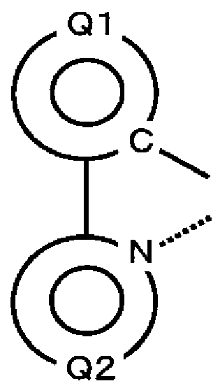





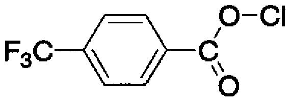


Claims
Priority Applications (5)
| Application Number | Priority Date | Filing Date | Title |
|---|---|---|---|
| EP06713643.2A EP1857521B2 (en) | 2005-02-21 | 2006-02-14 | Organic electric field light emitting element and production therefor |
| US11/816,672 US9365767B2 (en) | 2005-02-21 | 2006-02-14 | Organic electric field light emitting element and production therefor |
| KR1020077019151A KR101359288B1 (ko) | 2005-02-21 | 2006-02-14 | 유기 전계 발광 소자 및 그 제조 |
| US13/108,484 US20110215312A1 (en) | 2005-02-21 | 2011-05-16 | Organic electric field light emitting element and production therefor |
| US15/132,358 US9640769B2 (en) | 2005-02-21 | 2016-04-19 | Organic electric field light emitting element and production therefor |
Applications Claiming Priority (2)
| Application Number | Priority Date | Filing Date | Title |
|---|---|---|---|
| JP2005044250 | 2005-02-21 | ||
| JP2005-044250 | 2005-02-21 |
Related Child Applications (3)
| Application Number | Title | Priority Date | Filing Date |
|---|---|---|---|
| US11/816,672 A-371-Of-International US9365767B2 (en) | 2005-02-21 | 2006-02-14 | Organic electric field light emitting element and production therefor |
| US13/108,484 Continuation US20110215312A1 (en) | 2005-02-21 | 2011-05-16 | Organic electric field light emitting element and production therefor |
| US15/132,358 Continuation US9640769B2 (en) | 2005-02-21 | 2016-04-19 | Organic electric field light emitting element and production therefor |
Publications (1)
| Publication Number | Publication Date |
|---|---|
| WO2006095539A1 true WO2006095539A1 (ja) | 2006-09-14 |
Family
ID=36953141
Family Applications (1)
| Application Number | Title | Priority Date | Filing Date |
|---|---|---|---|
| PCT/JP2006/302502 Ceased WO2006095539A1 (ja) | 2005-02-21 | 2006-02-14 | 有機電界発光素子及びその製造 |
Country Status (7)
| Country | Link |
|---|---|
| US (3) | US9365767B2 (ja) |
| EP (1) | EP1857521B2 (ja) |
| JP (2) | JP5092248B2 (ja) |
| KR (1) | KR101359288B1 (ja) |
| CN (2) | CN101128560A (ja) |
| TW (1) | TWI440692B (ja) |
| WO (1) | WO2006095539A1 (ja) |
Cited By (18)
| Publication number | Priority date | Publication date | Assignee | Title |
|---|---|---|---|---|
| JP2007067383A (ja) * | 2005-08-04 | 2007-03-15 | Mitsubishi Chemicals Corp | 電荷輸送材料、有機電界発光素子用組成物及び有機電界発光素子 |
| JP2008112984A (ja) * | 2006-10-04 | 2008-05-15 | Mitsubishi Chemicals Corp | 低分子塗布型有機電界発光素子用の電荷輸送材料、有機電界発光素子用組成物、有機電界発光素子用薄膜および有機電界発光素子 |
| WO2009064026A1 (ja) * | 2007-11-16 | 2009-05-22 | Sumitomo Chemical Company, Limited | スリット状吐出口から塗工液を吐出する塗布法用の塗工液 |
| JP2009203468A (ja) * | 2008-01-28 | 2009-09-10 | Mitsubishi Chemicals Corp | 発光層材料およびこれを用いた発光層形成用組成物、有機電界発光素子、ならびに有機エレクトロルミネッセンスディスプレイ |
| EP1829871A4 (en) * | 2004-12-24 | 2009-12-16 | Pioneer Corp | ORGANIC COMPOUND, CHARGE TRANSPORT MATERIAL, AND ORGANIC ELECTROLUMINESCENT ELEMENT |
| EP1820801A4 (en) * | 2004-12-10 | 2009-12-23 | Pioneer Corp | ORGANIC COMPOUND, CHARGE TRANSPORT MATERIAL, AND ORGANIC ELECTROLUMINESCENT ELEMENT |
| US8093806B2 (en) * | 2007-06-20 | 2012-01-10 | Semiconductor Energy Laboratory Co., Ltd. | Light-emitting device, method for manufacturing the same, and electronic apparatus |
| EP1887640A4 (en) * | 2005-05-24 | 2012-04-04 | Pioneer Corp | ORGANIC ELECTROLUMINESCENCE ELEMENT |
| JP2012516848A (ja) * | 2009-02-03 | 2012-07-26 | 日東電工株式会社 | 有機発光ダイオードにおける両極性ホスト |
| US20120211735A1 (en) * | 2009-01-09 | 2012-08-23 | Mitsubishi Chemical Corporation | Organic el element and organic light-emitting device |
| US8568183B2 (en) | 2010-04-09 | 2013-10-29 | Mitsubishi Chemical Corporation | Process of producing organic electroluminescence element composition, organic electroluminescence element composition, process of producing organic electroluminescence element, organic electroluminescence element, organic EL display device and organic EL lighting |
| WO2015097894A1 (ja) * | 2013-12-27 | 2015-07-02 | パイオニア株式会社 | 発光素子及び発光素子の製造方法 |
| US9090819B2 (en) | 2009-06-24 | 2015-07-28 | Konica Minolta, Inc. | Organic electroluminescent element, display device, illuminating device and condensed polycyclic heterocyclic compound |
| US9328094B2 (en) | 2011-09-19 | 2016-05-03 | Nitto Denko Corporation | Substituted biaryl compounds for light-emitting devices |
| US9328086B2 (en) | 2010-09-16 | 2016-05-03 | Nitto Denko Corporation | Substituted bipyridines for use in organic light-emitting devices |
| US9515277B2 (en) | 2008-08-13 | 2016-12-06 | Mitsubishi Chemical Corporation | Organic electroluminescent element, organic EL display device and organic EL illumination |
| US9825235B2 (en) | 2013-07-19 | 2017-11-21 | Semiconductor Energy Laboratory Co., Ltd. | Organic compound, light-emitting element, display module, lighting module, light-emitting device, display device, lighting device, and electronic device |
| US12520720B2 (en) | 2018-08-27 | 2026-01-06 | Samsung Electronics Co., Ltd. | Heterocyclic compound and organic light-emitting device |
Families Citing this family (48)
| Publication number | Priority date | Publication date | Assignee | Title |
|---|---|---|---|---|
| JP5092248B2 (ja) * | 2005-02-21 | 2012-12-05 | 三菱化学株式会社 | 有機電界発光素子用組成物、有機電界発光素子用薄膜、有機電界発光素子用薄膜転写用部材、有機電界発光素子及び有機電界発光素子の製造方法 |
| US7651791B2 (en) | 2005-12-15 | 2010-01-26 | Idemitsu Kosan Co., Ltd. | Material for organic electroluminescence device and electroluminescence device employing the same |
| JP2007308557A (ja) * | 2006-05-17 | 2007-11-29 | Mitsubishi Chemicals Corp | 有機電界発光素子用組成物、及びこれを用いた有機電界発光素子 |
| JP2008258320A (ja) * | 2007-04-03 | 2008-10-23 | Mitsubishi Chemicals Corp | 有機電界発光素子 |
| JP4967864B2 (ja) * | 2007-07-06 | 2012-07-04 | 三菱化学株式会社 | 有機電界発光素子 |
| JP5487595B2 (ja) * | 2007-11-15 | 2014-05-07 | 三菱化学株式会社 | 有機電界発光素子用組成物および有機電界発光素子 |
| US8896201B2 (en) * | 2008-02-19 | 2014-11-25 | Samsung Display Co., Ltd. | Organic light emitting device |
| US20090208776A1 (en) * | 2008-02-19 | 2009-08-20 | General Electric Company | Organic optoelectronic device and method for manufacturing the same |
| KR100922757B1 (ko) * | 2008-02-19 | 2009-10-21 | 삼성모바일디스플레이주식회사 | 수명을 향상시킨 유기 발광 소자 |
| WO2009123763A2 (en) * | 2008-04-03 | 2009-10-08 | Qd Vision, Inc. | Light-emitting device including quantum dots |
| US9525148B2 (en) | 2008-04-03 | 2016-12-20 | Qd Vision, Inc. | Device including quantum dots |
| GB2462410B (en) * | 2008-07-21 | 2011-04-27 | Cambridge Display Tech Ltd | Compositions and methods for manufacturing light-emissive devices |
| KR20110036098A (ko) * | 2008-07-31 | 2011-04-06 | 미쓰비시 가가꾸 가부시키가이샤 | 유기 전계 발광 소자용 조성물, 유기 박막, 유기 전계 발광 소자, 유기 el 표시 장치 및 유기 el 조명 |
| JP5540600B2 (ja) * | 2008-08-13 | 2014-07-02 | 三菱化学株式会社 | 電子デバイス、有機電界発光素子、有機el表示装置および有機el照明 |
| GB2462653B (en) * | 2008-08-15 | 2013-03-20 | Cambridge Display Tech Ltd | Opto-electrical devices and methods of manufacturing the same |
| JP2010182637A (ja) | 2009-02-09 | 2010-08-19 | Fujifilm Corp | 有機電界発光素子の製造方法及び有機電界発光素子 |
| JP2010209320A (ja) * | 2009-02-13 | 2010-09-24 | Mitsubishi Chemicals Corp | 有機電界発光素子用組成物、有機電界発光素子の製造方法、有機電界発光素子、有機elディスプレイ及び有機el照明 |
| JP4599469B1 (ja) * | 2009-08-31 | 2010-12-15 | 富士フイルム株式会社 | 有機電界発光素子用材料及び有機電界発光素子 |
| JP5577685B2 (ja) * | 2009-12-15 | 2014-08-27 | 三菱化学株式会社 | 有機電界発光素子の製造方法、有機電界発光素子、有機el表示装置及び有機el照明 |
| CN102742354A (zh) * | 2010-02-05 | 2012-10-17 | 住友化学株式会社 | 有机电致发光元件、其制造方法及制造装置 |
| JP4579343B1 (ja) * | 2010-04-23 | 2010-11-10 | 富士フイルム株式会社 | 有機電界発光素子用材料及び有機電界発光素子 |
| KR101778825B1 (ko) * | 2010-05-03 | 2017-09-14 | 메르크 파텐트 게엠베하 | 제형물 및 전자 소자 |
| CN102869672B (zh) * | 2010-05-03 | 2016-05-11 | 默克专利有限公司 | 制剂和电子器件 |
| JP2012033918A (ja) * | 2010-07-08 | 2012-02-16 | Mitsubishi Chemicals Corp | 有機電界発光素子、有機電界発光デバイス、有機el表示装置及び有機el照明 |
| US8963415B2 (en) * | 2010-11-15 | 2015-02-24 | Panasonic Corporation | Organic EL element, display panel, and display device |
| US8435797B2 (en) * | 2010-12-07 | 2013-05-07 | The United States Of America As Represented By The Secretary Of The Army | Electroluminescent diode sensor |
| KR102136426B1 (ko) * | 2011-02-16 | 2020-07-21 | 가부시키가이샤 한도오따이 에네루기 켄큐쇼 | 발광 엘리먼트 |
| WO2012158252A1 (en) | 2011-05-16 | 2012-11-22 | Qd Vision, Inc. | Device including quantum dots and method for making same |
| CN103380508B (zh) | 2011-11-22 | 2017-09-08 | 出光兴产株式会社 | 芳香族杂环衍生物、有机电致发光元件用材料以及有机电致发光元件 |
| WO2013103440A1 (en) | 2012-01-06 | 2013-07-11 | Qd Vision, Inc. | Light emitting device including blue emitting quantum dots and method |
| US9698386B2 (en) | 2012-04-13 | 2017-07-04 | Oti Lumionics Inc. | Functionalization of a substrate |
| US8853070B2 (en) * | 2012-04-13 | 2014-10-07 | Oti Lumionics Inc. | Functionalization of a substrate |
| KR101434737B1 (ko) | 2012-08-10 | 2014-08-27 | 주식회사 두산 | 신규 화합물 및 이를 포함하는 유기 전계 발광 소자 |
| EP2917382A4 (en) | 2012-11-06 | 2016-07-06 | Oti Lumionics Inc | METHOD FOR DEPOSITING A CONDUCTIVE COATING ON A SURFACE |
| JP6428600B2 (ja) * | 2013-03-08 | 2018-11-28 | 日立化成株式会社 | イオン性化合物を含有する処理液、有機エレクトロニクス素子、及び有機エレクトロニクス素子の製造方法 |
| US9806294B2 (en) * | 2013-03-28 | 2017-10-31 | Konica Minolta, Inc. | Surface light emitting element |
| WO2016006243A1 (ja) * | 2014-07-10 | 2016-01-14 | 株式会社Joled | 有機el素子 |
| CN104269494B (zh) * | 2014-09-15 | 2017-05-03 | 京东方科技集团股份有限公司 | 有机电致发光器件及其制备方法、显示装置 |
| GB2539895B (en) * | 2015-06-29 | 2020-10-07 | Flexenable Ltd | Organic electronic/optoelectronic devices |
| US10355246B2 (en) | 2015-12-16 | 2019-07-16 | Oti Lumionics Inc. | Barrier coating for opto-electronics devices |
| WO2017130828A1 (ja) | 2016-01-28 | 2017-08-03 | 住友化学株式会社 | 膜の製造方法 |
| US11152587B2 (en) | 2016-08-15 | 2021-10-19 | Oti Lumionics Inc. | Light transmissive electrode for light emitting devices |
| US11046886B2 (en) | 2017-09-14 | 2021-06-29 | Sumitomo Chemical Company, Limited | Method for producing liquid composition |
| KR102285565B1 (ko) * | 2017-12-12 | 2021-08-04 | 주식회사 엘지화학 | 잉크 조성물 및 유기 발광 소자 제조방법 |
| US11985888B2 (en) * | 2019-08-12 | 2024-05-14 | The Regents Of The University Of Michigan | Organic electroluminescent device |
| WO2021235111A1 (ja) * | 2020-05-21 | 2021-11-25 | 株式会社島津製作所 | 分析データ管理システムにおける教師用データ生成方法 |
| WO2021263077A1 (en) * | 2020-06-26 | 2021-12-30 | Loyola University Chicago | Surface-modified electron transport layer of organic light-emitting diode |
| CN112802972A (zh) * | 2020-12-31 | 2021-05-14 | 湖南鼎一致远科技发展有限公司 | 一种聚碳酸酯基材的电致发光器件及制备方法 |
Citations (3)
| Publication number | Priority date | Publication date | Assignee | Title |
|---|---|---|---|---|
| US20040209115A1 (en) | 2003-04-21 | 2004-10-21 | Thompson Mark E. | Organic light emitting devices with wide gap host materials |
| US20040214040A1 (en) | 2002-12-30 | 2004-10-28 | Soo-Hyoung Lee | Biphenyl derivatives and organic electroluminescent device employing the same |
| JP2006073992A (ja) * | 2004-05-20 | 2006-03-16 | Semiconductor Energy Lab Co Ltd | 発光素子および発光装置 |
Family Cites Families (28)
| Publication number | Priority date | Publication date | Assignee | Title |
|---|---|---|---|---|
| JP3069139B2 (ja) | 1990-03-16 | 2000-07-24 | 旭化成工業株式会社 | 分散型電界発光素子 |
| US6303238B1 (en) * | 1997-12-01 | 2001-10-16 | The Trustees Of Princeton University | OLEDs doped with phosphorescent compounds |
| JPH11251060A (ja) | 1998-02-27 | 1999-09-17 | Fuji Photo Film Co Ltd | エレクトロルミネッセンス素子 |
| JPH11273859A (ja) | 1998-03-24 | 1999-10-08 | Sony Corp | 有機電界発光素子及びその製造方法 |
| US6366017B1 (en) * | 1999-07-14 | 2002-04-02 | Agilent Technologies, Inc/ | Organic light emitting diodes with distributed bragg reflector |
| TWI263636B (en) * | 1999-09-16 | 2006-10-11 | Ciba Sc Holding Ag | Fluorescent maleimides and use thereof |
| JP4154139B2 (ja) * | 2000-09-26 | 2008-09-24 | キヤノン株式会社 | 発光素子 |
| KR100865096B1 (ko) * | 2000-11-30 | 2008-10-24 | 캐논 가부시끼가이샤 | 발광 소자 및 표시 장치 |
| JP2003045666A (ja) * | 2001-05-23 | 2003-02-14 | Honda Motor Co Ltd | 有機エレクトロルミネッセンス素子 |
| JP2003187972A (ja) * | 2001-12-20 | 2003-07-04 | Dainippon Printing Co Ltd | 有機el素子の製造方法および有機el転写体と被転写体 |
| JP2003192691A (ja) * | 2001-12-26 | 2003-07-09 | Mitsubishi Chemicals Corp | 有機イリジウム錯体及び有機電界発光素子 |
| US6863997B2 (en) * | 2001-12-28 | 2005-03-08 | The Trustees Of Princeton University | White light emitting OLEDs from combined monomer and aggregate emission |
| US7990046B2 (en) * | 2002-03-15 | 2011-08-02 | Idemitsu Kosan Co., Ltd. | Material for organic electroluminescent devices and organic electroluminescent devices made by using the same |
| JP3902981B2 (ja) * | 2002-06-04 | 2007-04-11 | キヤノン株式会社 | 有機発光素子及び表示装置 |
| DE10232238A1 (de) | 2002-07-17 | 2004-02-05 | Philips Intellectual Property & Standards Gmbh | Elektrolumineszierende Vorrichtung aus zweidimensionalem Array |
| GB0220080D0 (en) | 2002-08-29 | 2002-10-09 | Isis Innovation | Blended dendrimers |
| US20040096570A1 (en) * | 2002-11-15 | 2004-05-20 | Michael Weaver | Structure and method of fabricating organic devices |
| JP2004277377A (ja) | 2003-03-18 | 2004-10-07 | Junji Kido | フルオレン系化合物、およびこれを用いた有機電界発光素子 |
| AU2003252733A1 (en) | 2003-07-30 | 2005-02-15 | Nihon University | Pearl core regenerating method and device |
| KR100994083B1 (ko) * | 2003-07-31 | 2010-11-12 | 미쓰비시 가가꾸 가부시키가이샤 | 화합물, 전하 수송 재료 및 유기 전계 발광 소자 |
| DE10338550A1 (de) | 2003-08-19 | 2005-03-31 | Basf Ag | Übergangsmetallkomplexe mit Carbenliganden als Emitter für organische Licht-emittierende Dioden (OLEDs) |
| JP4674454B2 (ja) | 2004-01-27 | 2011-04-20 | ソニー株式会社 | 有機発光材料および有機電界発光素子 |
| JP2005272805A (ja) | 2004-02-24 | 2005-10-06 | Sony Corp | 有機材料および有機電界発光素子 |
| JP4618414B2 (ja) | 2004-02-24 | 2011-01-26 | ソニー株式会社 | 有機材料および有機電界発光素子 |
| US7811677B2 (en) * | 2004-05-20 | 2010-10-12 | Semiconductor Energy Laboratory Co., Ltd. | Light emitting element and light emitting device |
| JP5092248B2 (ja) * | 2005-02-21 | 2012-12-05 | 三菱化学株式会社 | 有機電界発光素子用組成物、有機電界発光素子用薄膜、有機電界発光素子用薄膜転写用部材、有機電界発光素子及び有機電界発光素子の製造方法 |
| US7733009B2 (en) | 2006-04-27 | 2010-06-08 | Global Oled Technology Llc | Electroluminescent device including an anthracene derivative |
| US20090191427A1 (en) * | 2008-01-30 | 2009-07-30 | Liang-Sheng Liao | Phosphorescent oled having double hole-blocking layers |
-
2006
- 2006-02-14 JP JP2006036880A patent/JP5092248B2/ja not_active Expired - Lifetime
- 2006-02-14 CN CNA2006800056015A patent/CN101128560A/zh active Pending
- 2006-02-14 US US11/816,672 patent/US9365767B2/en active Active
- 2006-02-14 CN CN2010102687015A patent/CN101955771B/zh not_active Expired - Lifetime
- 2006-02-14 KR KR1020077019151A patent/KR101359288B1/ko not_active Expired - Lifetime
- 2006-02-14 EP EP06713643.2A patent/EP1857521B2/en not_active Expired - Lifetime
- 2006-02-14 WO PCT/JP2006/302502 patent/WO2006095539A1/ja not_active Ceased
- 2006-02-21 TW TW095105720A patent/TWI440692B/zh not_active IP Right Cessation
-
2009
- 2009-02-09 JP JP2009027021A patent/JP5428367B2/ja not_active Expired - Lifetime
-
2011
- 2011-05-16 US US13/108,484 patent/US20110215312A1/en not_active Abandoned
-
2016
- 2016-04-19 US US15/132,358 patent/US9640769B2/en not_active Expired - Lifetime
Patent Citations (3)
| Publication number | Priority date | Publication date | Assignee | Title |
|---|---|---|---|---|
| US20040214040A1 (en) | 2002-12-30 | 2004-10-28 | Soo-Hyoung Lee | Biphenyl derivatives and organic electroluminescent device employing the same |
| US20040209115A1 (en) | 2003-04-21 | 2004-10-21 | Thompson Mark E. | Organic light emitting devices with wide gap host materials |
| JP2006073992A (ja) * | 2004-05-20 | 2006-03-16 | Semiconductor Energy Lab Co Ltd | 発光素子および発光装置 |
Non-Patent Citations (4)
| Title |
|---|
| G. HE ET AL., APPL. PHYS. LETT., vol. 85, 2004, pages 3911 |
| S. OKADA ET AL., SID 2002 DIGEST, 2002, pages 1360 |
| See also references of EP1857521A4 |
| THOMPSON M.E.: "Efficient utilization of excitons", NSF WORKSHOP ON FUNDAMENTAL RESEARCH NEEDS IN PHOTONIC MATERIALS SYNTHESIS AND PROCESSING AT THE INTERFACE, 29 April 2003 (2003-04-29), XP008136319, Retrieved from the Internet <URL:http://www.rochester.edu/College/workshop/presentations/MartThompson/MT_2003.ppt#615,25,FIr6> * |
Cited By (23)
| Publication number | Priority date | Publication date | Assignee | Title |
|---|---|---|---|---|
| EP1820801A4 (en) * | 2004-12-10 | 2009-12-23 | Pioneer Corp | ORGANIC COMPOUND, CHARGE TRANSPORT MATERIAL, AND ORGANIC ELECTROLUMINESCENT ELEMENT |
| EP1829871A4 (en) * | 2004-12-24 | 2009-12-16 | Pioneer Corp | ORGANIC COMPOUND, CHARGE TRANSPORT MATERIAL, AND ORGANIC ELECTROLUMINESCENT ELEMENT |
| EP1887640A4 (en) * | 2005-05-24 | 2012-04-04 | Pioneer Corp | ORGANIC ELECTROLUMINESCENCE ELEMENT |
| US8933622B2 (en) | 2005-05-24 | 2015-01-13 | Pioneer Corporation | Organic electroluminescence element |
| JP2007067383A (ja) * | 2005-08-04 | 2007-03-15 | Mitsubishi Chemicals Corp | 電荷輸送材料、有機電界発光素子用組成物及び有機電界発光素子 |
| JP2008112984A (ja) * | 2006-10-04 | 2008-05-15 | Mitsubishi Chemicals Corp | 低分子塗布型有機電界発光素子用の電荷輸送材料、有機電界発光素子用組成物、有機電界発光素子用薄膜および有機電界発光素子 |
| US8368301B2 (en) | 2007-06-20 | 2013-02-05 | Semiconductor Energy Laboratory Co., Ltd. | Light-emitting device, method for manufacturing the same, and electronic apparatus |
| US8093806B2 (en) * | 2007-06-20 | 2012-01-10 | Semiconductor Energy Laboratory Co., Ltd. | Light-emitting device, method for manufacturing the same, and electronic apparatus |
| US8531104B2 (en) | 2007-06-20 | 2013-09-10 | Semiconductor Energy Laboratory Co., Ltd. | Light-emitting device, method for manufacturing the same, and electronic apparatus |
| WO2009064026A1 (ja) * | 2007-11-16 | 2009-05-22 | Sumitomo Chemical Company, Limited | スリット状吐出口から塗工液を吐出する塗布法用の塗工液 |
| JP2009203468A (ja) * | 2008-01-28 | 2009-09-10 | Mitsubishi Chemicals Corp | 発光層材料およびこれを用いた発光層形成用組成物、有機電界発光素子、ならびに有機エレクトロルミネッセンスディスプレイ |
| US9515277B2 (en) | 2008-08-13 | 2016-12-06 | Mitsubishi Chemical Corporation | Organic electroluminescent element, organic EL display device and organic EL illumination |
| US20120211735A1 (en) * | 2009-01-09 | 2012-08-23 | Mitsubishi Chemical Corporation | Organic el element and organic light-emitting device |
| JP2012516848A (ja) * | 2009-02-03 | 2012-07-26 | 日東電工株式会社 | 有機発光ダイオードにおける両極性ホスト |
| US9090819B2 (en) | 2009-06-24 | 2015-07-28 | Konica Minolta, Inc. | Organic electroluminescent element, display device, illuminating device and condensed polycyclic heterocyclic compound |
| US8568183B2 (en) | 2010-04-09 | 2013-10-29 | Mitsubishi Chemical Corporation | Process of producing organic electroluminescence element composition, organic electroluminescence element composition, process of producing organic electroluminescence element, organic electroluminescence element, organic EL display device and organic EL lighting |
| US9328086B2 (en) | 2010-09-16 | 2016-05-03 | Nitto Denko Corporation | Substituted bipyridines for use in organic light-emitting devices |
| US9328094B2 (en) | 2011-09-19 | 2016-05-03 | Nitto Denko Corporation | Substituted biaryl compounds for light-emitting devices |
| US9825235B2 (en) | 2013-07-19 | 2017-11-21 | Semiconductor Energy Laboratory Co., Ltd. | Organic compound, light-emitting element, display module, lighting module, light-emitting device, display device, lighting device, and electronic device |
| WO2015097894A1 (ja) * | 2013-12-27 | 2015-07-02 | パイオニア株式会社 | 発光素子及び発光素子の製造方法 |
| JPWO2015097894A1 (ja) * | 2013-12-27 | 2017-03-23 | パイオニア株式会社 | 発光素子及び発光素子の製造方法 |
| US9876188B2 (en) | 2013-12-27 | 2018-01-23 | Pioneer Corporation | Light emitting element and method of manufacturing light emitting element |
| US12520720B2 (en) | 2018-08-27 | 2026-01-06 | Samsung Electronics Co., Ltd. | Heterocyclic compound and organic light-emitting device |
Also Published As
| Publication number | Publication date |
|---|---|
| US9365767B2 (en) | 2016-06-14 |
| EP1857521B1 (en) | 2014-04-02 |
| KR101359288B1 (ko) | 2014-02-10 |
| TWI440692B (zh) | 2014-06-11 |
| JP5428367B2 (ja) | 2014-02-26 |
| TW200702420A (en) | 2007-01-16 |
| CN101955771B (zh) | 2012-08-22 |
| US20090066223A1 (en) | 2009-03-12 |
| US9640769B2 (en) | 2017-05-02 |
| US20160233445A1 (en) | 2016-08-11 |
| EP1857521A4 (en) | 2010-03-17 |
| EP1857521A1 (en) | 2007-11-21 |
| JP2009102656A (ja) | 2009-05-14 |
| EP1857521B2 (en) | 2021-12-22 |
| JP2006257409A (ja) | 2006-09-28 |
| US20110215312A1 (en) | 2011-09-08 |
| KR20070110498A (ko) | 2007-11-19 |
| JP5092248B2 (ja) | 2012-12-05 |
| CN101955771A (zh) | 2011-01-26 |
| CN101128560A (zh) | 2008-02-20 |
Similar Documents
| Publication | Publication Date | Title |
|---|---|---|
| JP5092248B2 (ja) | 有機電界発光素子用組成物、有機電界発光素子用薄膜、有機電界発光素子用薄膜転写用部材、有機電界発光素子及び有機電界発光素子の製造方法 | |
| JP4770843B2 (ja) | 有機電界発光素子及び有機デバイスの製造方法 | |
| JP5088097B2 (ja) | 有機電界蛍光発光素子用材料、有機電界蛍光発光素子用組成物、有機電界蛍光発光素子、有機elディスプレイ及びカラーディスプレイ表示装置 | |
| CN104365180B (zh) | 导电性薄膜积层体的制造方法 | |
| JP4893173B2 (ja) | 有機電界発光素子用組成物及び有機電界発光素子 | |
| WO2010016555A1 (ja) | 重合体、発光層材料、有機電界発光素子材料、有機電界発光素子用組成物、これらを利用した有機電界発光素子、太陽電池素子、有機el表示装置、及び有機el照明 | |
| JP5884213B2 (ja) | 有機電界発光素子の製造方法、有機電界発光素子、有機elディスプレイ及び有機el照明 | |
| EP2557898B1 (en) | Method of producing a composition for use in an organic electroluminescent element | |
| WO2011024922A1 (ja) | モノアミン化合物、電荷輸送材料、電荷輸送膜用組成物、有機電界発光素子、有機el表示装置及び有機el照明 | |
| JP4910741B2 (ja) | 有機電界発光素子の製造方法 | |
| TW201833298A (zh) | 發光層形成用組成物以及含有該發光層形成用組成物的有機電場發光元件 | |
| JP5708426B2 (ja) | 有機電界発光素子用組成物及び有機電界発光素子 | |
| JP2007335852A (ja) | 電荷輸送材料、有機電界発光素子用組成物、有機電界発光素子用薄膜および有機電界発光素子 | |
| JP2010229121A (ja) | 有機金属錯体、有機電界発光素子用組成物および有機電界発光素子 | |
| JP2007100083A (ja) | 有機電界発光素子用組成物及び有機電界発光素子 | |
| JP5098199B2 (ja) | 高分子化合物、有機電界発光素子用組成物、有機電界発光素子用薄膜および有機電界発光素子 | |
| JP2014197696A (ja) | 有機電界発光素子用組成物 | |
| JP2007308557A (ja) | 有機電界発光素子用組成物、及びこれを用いた有機電界発光素子 |
Legal Events
| Date | Code | Title | Description |
|---|---|---|---|
| 121 | Ep: the epo has been informed by wipo that ep was designated in this application | ||
| WWE | Wipo information: entry into national phase |
Ref document number: 2006713643 Country of ref document: EP Ref document number: 11816672 Country of ref document: US |
|
| WWE | Wipo information: entry into national phase |
Ref document number: 200680005601.5 Country of ref document: CN Ref document number: 1020077019151 Country of ref document: KR |
|
| NENP | Non-entry into the national phase |
Ref country code: DE |
|
| WWP | Wipo information: published in national office |
Ref document number: 2006713643 Country of ref document: EP |