WO2006106883A1 - 蛍光体、蛍光体シートおよびその製造方法、並びに当該蛍光体を用いた発光装置 - Google Patents

蛍光体、蛍光体シートおよびその製造方法、並びに当該蛍光体を用いた発光装置 Download PDF

Info

Publication number
WO2006106883A1
WO2006106883A1 PCT/JP2006/306756 JP2006306756W WO2006106883A1 WO 2006106883 A1 WO2006106883 A1 WO 2006106883A1 JP 2006306756 W JP2006306756 W JP 2006306756W WO 2006106883 A1 WO2006106883 A1 WO 2006106883A1
Authority
WO
WIPO (PCT)
Prior art keywords
phosphor
light
firing
wavelength
emitting device
Prior art date
Legal status (The legal status is an assumption and is not a legal conclusion. Google has not performed a legal analysis and makes no representation as to the accuracy of the status listed.)
Ceased
Application number
PCT/JP2006/306756
Other languages
English (en)
French (fr)
Inventor
Akira Nagatomi
Kenji Sakane
Current Assignee (The listed assignees may be inaccurate. Google has not performed a legal analysis and makes no representation or warranty as to the accuracy of the list.)
Dowa Holdings Co Ltd
Dowa Electronics Materials Co Ltd
Original Assignee
Dowa Electronics Materials Co Ltd
Dowa Mining Co Ltd
Priority date (The priority date is an assumption and is not a legal conclusion. Google has not performed a legal analysis and makes no representation as to the accuracy of the date listed.)
Filing date
Publication date
Application filed by Dowa Electronics Materials Co Ltd, Dowa Mining Co Ltd filed Critical Dowa Electronics Materials Co Ltd
Priority to EP06730704A priority Critical patent/EP1878778A4/en
Priority to US11/887,654 priority patent/US8048338B2/en
Priority to JP2007512901A priority patent/JPWO2006106883A1/ja
Publication of WO2006106883A1 publication Critical patent/WO2006106883A1/ja
Anticipated expiration legal-status Critical
Ceased legal-status Critical Current

Links

Classifications

    • CCHEMISTRY; METALLURGY
    • C09DYES; PAINTS; POLISHES; NATURAL RESINS; ADHESIVES; COMPOSITIONS NOT OTHERWISE PROVIDED FOR; APPLICATIONS OF MATERIALS NOT OTHERWISE PROVIDED FOR
    • C09KMATERIALS FOR MISCELLANEOUS APPLICATIONS, NOT PROVIDED FOR ELSEWHERE
    • C09K11/00Luminescent materials, e.g. electroluminescent or chemiluminescent
    • C09K11/08Luminescent materials, e.g. electroluminescent or chemiluminescent containing inorganic luminescent materials
    • C09K11/0883Arsenides; Nitrides; Phosphides
    • CCHEMISTRY; METALLURGY
    • C09DYES; PAINTS; POLISHES; NATURAL RESINS; ADHESIVES; COMPOSITIONS NOT OTHERWISE PROVIDED FOR; APPLICATIONS OF MATERIALS NOT OTHERWISE PROVIDED FOR
    • C09KMATERIALS FOR MISCELLANEOUS APPLICATIONS, NOT PROVIDED FOR ELSEWHERE
    • C09K11/00Luminescent materials, e.g. electroluminescent or chemiluminescent
    • C09K11/08Luminescent materials, e.g. electroluminescent or chemiluminescent containing inorganic luminescent materials
    • C09K11/77Luminescent materials, e.g. electroluminescent or chemiluminescent containing inorganic luminescent materials containing rare earth metals
    • C09K11/7715Luminescent materials, e.g. electroluminescent or chemiluminescent containing inorganic luminescent materials containing rare earth metals containing cerium
    • C09K11/77218Silicon Aluminium Nitrides or Silicon Aluminium Oxynitrides
    • CCHEMISTRY; METALLURGY
    • C09DYES; PAINTS; POLISHES; NATURAL RESINS; ADHESIVES; COMPOSITIONS NOT OTHERWISE PROVIDED FOR; APPLICATIONS OF MATERIALS NOT OTHERWISE PROVIDED FOR
    • C09KMATERIALS FOR MISCELLANEOUS APPLICATIONS, NOT PROVIDED FOR ELSEWHERE
    • C09K11/00Luminescent materials, e.g. electroluminescent or chemiluminescent
    • C09K11/08Luminescent materials, e.g. electroluminescent or chemiluminescent containing inorganic luminescent materials
    • C09K11/55Luminescent materials, e.g. electroluminescent or chemiluminescent containing inorganic luminescent materials containing beryllium, magnesium, alkali metals or alkaline earth metals
    • CCHEMISTRY; METALLURGY
    • C09DYES; PAINTS; POLISHES; NATURAL RESINS; ADHESIVES; COMPOSITIONS NOT OTHERWISE PROVIDED FOR; APPLICATIONS OF MATERIALS NOT OTHERWISE PROVIDED FOR
    • C09KMATERIALS FOR MISCELLANEOUS APPLICATIONS, NOT PROVIDED FOR ELSEWHERE
    • C09K11/00Luminescent materials, e.g. electroluminescent or chemiluminescent
    • C09K11/08Luminescent materials, e.g. electroluminescent or chemiluminescent containing inorganic luminescent materials
    • C09K11/77Luminescent materials, e.g. electroluminescent or chemiluminescent containing inorganic luminescent materials containing rare earth metals
    • C09K11/7728Luminescent materials, e.g. electroluminescent or chemiluminescent containing inorganic luminescent materials containing rare earth metals containing europium
    • C09K11/77347Silicon Nitrides or Silicon Oxynitrides
    • CCHEMISTRY; METALLURGY
    • C09DYES; PAINTS; POLISHES; NATURAL RESINS; ADHESIVES; COMPOSITIONS NOT OTHERWISE PROVIDED FOR; APPLICATIONS OF MATERIALS NOT OTHERWISE PROVIDED FOR
    • C09KMATERIALS FOR MISCELLANEOUS APPLICATIONS, NOT PROVIDED FOR ELSEWHERE
    • C09K11/00Luminescent materials, e.g. electroluminescent or chemiluminescent
    • C09K11/08Luminescent materials, e.g. electroluminescent or chemiluminescent containing inorganic luminescent materials
    • C09K11/77Luminescent materials, e.g. electroluminescent or chemiluminescent containing inorganic luminescent materials containing rare earth metals
    • C09K11/7728Luminescent materials, e.g. electroluminescent or chemiluminescent containing inorganic luminescent materials containing rare earth metals containing europium
    • C09K11/77348Silicon Aluminium Nitrides or Silicon Aluminium Oxynitrides
    • CCHEMISTRY; METALLURGY
    • C09DYES; PAINTS; POLISHES; NATURAL RESINS; ADHESIVES; COMPOSITIONS NOT OTHERWISE PROVIDED FOR; APPLICATIONS OF MATERIALS NOT OTHERWISE PROVIDED FOR
    • C09KMATERIALS FOR MISCELLANEOUS APPLICATIONS, NOT PROVIDED FOR ELSEWHERE
    • C09K11/00Luminescent materials, e.g. electroluminescent or chemiluminescent
    • C09K11/08Luminescent materials, e.g. electroluminescent or chemiluminescent containing inorganic luminescent materials
    • C09K11/77Luminescent materials, e.g. electroluminescent or chemiluminescent containing inorganic luminescent materials containing rare earth metals
    • C09K11/7728Luminescent materials, e.g. electroluminescent or chemiluminescent containing inorganic luminescent materials containing rare earth metals containing europium
    • C09K11/7737Phosphates
    • C09K11/7738Phosphates with alkaline earth metals
    • C09K11/7739Phosphates with alkaline earth metals with halogens
    • HELECTRICITY
    • H10SEMICONDUCTOR DEVICES; ELECTRIC SOLID-STATE DEVICES NOT OTHERWISE PROVIDED FOR
    • H10HINORGANIC LIGHT-EMITTING SEMICONDUCTOR DEVICES HAVING POTENTIAL BARRIERS
    • H10H20/00Individual inorganic light-emitting semiconductor devices having potential barriers, e.g. light-emitting diodes [LED]
    • H10H20/80Constructional details
    • H10H20/85Packages
    • H10H20/851Wavelength conversion means
    • H10H20/8511Wavelength conversion means characterised by their material, e.g. binder
    • H10H20/8512Wavelength conversion materials
    • HELECTRICITY
    • H10SEMICONDUCTOR DEVICES; ELECTRIC SOLID-STATE DEVICES NOT OTHERWISE PROVIDED FOR
    • H10WGENERIC PACKAGES, INTERCONNECTIONS, CONNECTORS OR OTHER CONSTRUCTIONAL DETAILS OF DEVICES COVERED BY CLASS H10
    • H10W72/00Interconnections or connectors in packages
    • H10W72/01Manufacture or treatment
    • H10W72/015Manufacture or treatment of bond wires
    • H10W72/01515Forming coatings
    • HELECTRICITY
    • H10SEMICONDUCTOR DEVICES; ELECTRIC SOLID-STATE DEVICES NOT OTHERWISE PROVIDED FOR
    • H10WGENERIC PACKAGES, INTERCONNECTIONS, CONNECTORS OR OTHER CONSTRUCTIONAL DETAILS OF DEVICES COVERED BY CLASS H10
    • H10W72/00Interconnections or connectors in packages
    • H10W72/071Connecting or disconnecting
    • H10W72/075Connecting or disconnecting of bond wires
    • HELECTRICITY
    • H10SEMICONDUCTOR DEVICES; ELECTRIC SOLID-STATE DEVICES NOT OTHERWISE PROVIDED FOR
    • H10WGENERIC PACKAGES, INTERCONNECTIONS, CONNECTORS OR OTHER CONSTRUCTIONAL DETAILS OF DEVICES COVERED BY CLASS H10
    • H10W74/00Encapsulations, e.g. protective coatings
    • HELECTRICITY
    • H10SEMICONDUCTOR DEVICES; ELECTRIC SOLID-STATE DEVICES NOT OTHERWISE PROVIDED FOR
    • H10WGENERIC PACKAGES, INTERCONNECTIONS, CONNECTORS OR OTHER CONSTRUCTIONAL DETAILS OF DEVICES COVERED BY CLASS H10
    • H10W90/00Package configurations
    • H10W90/701Package configurations characterised by the relative positions of pads or connectors relative to package parts
    • H10W90/751Package configurations characterised by the relative positions of pads or connectors relative to package parts of bond wires
    • H10W90/756Package configurations characterised by the relative positions of pads or connectors relative to package parts of bond wires between a chip and a stacked lead frame, conducting package substrate or heat sink

Definitions

  • the present invention relates to a display such as a cathode ray tube (CRT), a field emission display (FED), and a plasma display (PDP), a lighting device such as a fluorescent lamp and a fluorescent display tube, and a light emitting device such as a liquid crystal backlight.
  • the present invention relates to a phosphor containing nitrogen, a phosphor sheet and a method for producing the same, and a light emitting device such as a white LED illumination in which a semiconductor light emitting element (LED) and the phosphor are combined.
  • this white LED lighting is put to practical use, it will have high efficiency in converting electrical energy into light and generate less heat, and since it is composed of LED and phosphor power, it can be cut like a conventional incandescent bulb. It has the advantages of long life, no harmful substances such as mercury, and the miniaturization of the lighting device, resulting in an ideal lighting device.
  • the white LED lighting method that produces white light by combining this high-brightness LED with a phosphor is called the one-chip type, and uses three primary colors: a high-brightness red LED, green LED, and blue LED. Compared to the multi-chip type method that produces white color by using it, it has excellent color rendering properties and can be manufactured at low cost.
  • One-chip type white LED lighting includes a combination of a high-intensity blue LED and a phosphor that emits yellow light when excited by the blue light generated by the LED power.
  • High-intensity blue LED and garnet-based yellow phosphor (Y, Gd ) (Al, Ga) O: Ce (YAG: Ce), Tb Al O: Ce ⁇ Ca Sc Si O: Ce, etc.
  • This white LED lighting makes use of the fact that the blue and yellow colors of light are complementary.
  • this white LED illumination was high in brightness, there was a problem that the color rendering, which is important for illumination, was poor because the long-wavelength side emission in the visible light region, that is, the red component, was insufficient.
  • the developed phosphors are developed one after another, and the color rendering properties are improved by adding this phosphor.
  • the phosphor containing nitrogen is, for example, Ca Si N: Eu, Sr Si N: Eu, Ba Si N: Eu, Ca (Al, Si) (O, N): E
  • AlSiN: Eu is typical.
  • white LED lighting combining a high-intensity blue LED and a garnet-based yellow phosphor does not have a flat excitation band near the excitation wavelength of 460 nm.
  • the emission intensity and peak wavelength of LED varies, and when a phosphor is applied on the LED, the emission intensity of blue light that is transmitted changes depending on the film thickness. The balance of white light will be lost and the color of white light will change.
  • the near-ultraviolet LED emits light, and red (R) light is excited by the near-ultraviolet and ultraviolet light generated by the LED force.
  • RGB red
  • R'G'B red
  • mixing ratio etc.
  • the phosphor used in the application is a red phosphor, for example, Y
  • Ga 2 O Eu
  • a green phosphor for example, ZnS: Cu, Al, CaGaS: Eu
  • UV has a high-efficiency excitation band, and the emission spectrum has a broad peak. Brightness and color rendering are also improved in white LED lighting. However, there is no high-efficiency, high-brightness R'G'B or other phosphors like the YAG: Ce phosphor used in combination with high-intensity blue LEDs and garnet-based yellow phosphors. White LED lighting has not been obtained.
  • Patent Document 1 Japanese Patent Laid-Open No. 2003-96446
  • the nitrogen-containing phosphor of Patent Document 1 described above is a blue phosphor having a peak emission spectrum, but is excited by near-ultraviolet light. In this case, sufficient light emission intensity and brightness to satisfy a satisfactory level of light emission can not be obtained, so that it is considered insufficient for use in a light emitting device.
  • the object of the present invention has been made in consideration of the above-mentioned problems, and is a blue range (peak New phosphors and phosphor sheets with a broad emission spectrum (wavelength power of 00 nm to 500 nm) and a wide and flat excitation band in the near ultraviolet 'ultraviolet range' It is an object of the present invention to provide a manufacturing method and a light emitting device such as white LED illumination using the phosphor.
  • the present invention has advanced research on phosphor compositions containing various types of nitrogen, and as a result, optimized constituent elements, molar ratios of constituent elements, firing conditions, and the like.
  • a novel blue phosphor containing nitrogen represented by the following general formula was obtained.
  • a first configuration for solving the above-described problem is as follows.
  • the phosphor has a maximum peak wavelength in the emission spectrum in the range of 400 nm to 500 nm.
  • a second configuration is the phosphor according to the first configuration
  • a fourth configuration is the phosphor according to any one of the first to third configurations
  • the maximum emission intensity in the range of 400 ⁇ m and 500 ⁇ m is ⁇ , and the minimum emission intensity is P. It is a phosphor characterized by having ZP of 30% or more.
  • a fifth configuration is the phosphor according to any one of the first to fourth configurations,
  • M element is Mg, Ca, Sr, Ba, Zn, a rare earth element having a valence of II, and one or more elements selected by force,
  • a element is Al, Ga, In, Tl, ⁇ , Sc, ⁇ , As, Sb, Bi, force One or more selected elements,
  • B element is one or more elements selected from Si, Ge, Sn, Ti, Hf, Mo, W, Cr, Pb, Zr,
  • Z element is a phosphor characterized in that it is one or more elements selected from rare earth elements and transition metal element forces.
  • a sixth configuration is the phosphor according to any one of the first to fifth configurations,
  • M element is one or more elements selected from Mg, Ca, Sr, Ba, Zn
  • a element is one or more elements selected from Al, Ga, In force
  • B element is Si and Z or Ge
  • the Z element is a phosphor characterized in that it is one or more elements selected from Eu, Ce, Pr, Tb, Yb, and Mn.
  • a seventh configuration is the phosphor according to any one of the first to sixth configurations.
  • the phosphor is characterized in that M element is Sr, A element is A1, B element is Si, and Z element is Eu.
  • An eighth configuration is the phosphor according to any one of the first to seventh configurations,
  • a ninth configuration is the phosphor according to any one of the first to eighth configurations.
  • a tenth configuration is the phosphor according to any one of the first to ninth configurations,
  • the strongest diffraction peak is shown when the Bragg angle (2 0) is in the range of 35 ° force and 37 °.
  • the Bragg angle (2 0) of the diffraction pattern is in the range of 23.6 ° force to 25.6 °, 33 ° to 35 °, 39.7 ° force to 40.7 °, 43 ° force to 44 °, Two, two, one, and one characteristic diffraction peak can be seen, and the relative intensity of the strongest diffraction peak is 100% with a Bragg angle (2 0) in the range of 35 ° force and 37 °.
  • the relative intensity of these diffraction peaks is 2.0% or more and 40% or less.
  • An eleventh configuration is the phosphor according to any one of the first to tenth configurations
  • the phosphor of the product phase contained in the phosphor has a rhombic structure.
  • a twelfth configuration is the phosphor according to any one of the first to eleventh configurations
  • a thirteenth configuration is the phosphor according to any one of the first to eleventh configurations
  • the phosphor is characterized in that the unit volume of the crystal lattice of the product phase contained in the phosphor is 353A 3 or more and 385A 3 or less.
  • a fourteenth configuration is the phosphor according to any one of the first to thirteenth configurations
  • the lattice constant of the crystal lattice of the product phase contained in the phosphor is 7.85A or more, 8.28A or less, b is 9.26A or more, 9.58A or less, c is 4.80A or more, 4. It is a phosphor characterized by being 92A or less.
  • a fifteenth configuration is the phosphor according to any one of the first to fourteenth configurations
  • the phosphor is characterized by having a crystallite size (Dx) force of 50 nm or more contained in the phosphor particles.
  • a sixteenth configuration is the phosphor according to any one of the first to fourteenth configurations
  • the phosphor is characterized in that the crystallite size (Dx) of the product phase contained in the phosphor particles is 80 nm or more.
  • a seventeenth configuration is the phosphor according to any one of the first to sixteenth configurations,
  • the average particle diameter (D50) of the phosphor particles containing primary particles having a particle size of 50 m or less and aggregates in which the primary particles are aggregated and containing the primary particles and aggregates is 1. O / zm
  • the phosphor is characterized by being 50 ⁇ m or less.
  • An eighteenth configuration is the method of manufacturing a phosphor according to any one of the first to seventeenth configurations
  • the atmosphere gas at the time of firing is an inert gas such as nitrogen or a rare gas, ammonia, a mixed gas of ammonia and nitrogen, or a mixture of nitrogen and hydrogen.
  • an inert gas such as nitrogen or a rare gas, ammonia, a mixed gas of ammonia and nitrogen, or a mixture of nitrogen and hydrogen.
  • a nineteenth configuration is a method of manufacturing a phosphor according to the eighteenth configuration
  • the phosphor manufacturing method is characterized in that a gas containing 80% or more of nitrogen gas is used as the atmosphere gas in the furnace.
  • a twentieth configuration is a method of manufacturing a phosphor according to the eighteenth or nineteenth configuration, wherein the mixture is baked in a baking furnace to obtain a baked product.
  • the mixture is fired twice or more, and the fired mixture is pulverized and mixed between the firing.
  • a twenty-first configuration is a method for manufacturing a phosphor according to any of the eighteenth to twentieth configurations
  • the step of firing the mixture in a firing furnace to obtain a fired product and firing while allowing the atmosphere gas in the firing furnace to flow in an amount of 0.1 mlZmin or more.
  • a twenty-second configuration is a method of manufacturing a phosphor according to the twenty-first configuration, wherein first, firing is performed while circulating an atmosphere gas in the firing furnace at 0.1 lmlZmin or more, and then It is a method for producing a phosphor, characterized in that firing is performed without circulation of atmospheric gas in the firing furnace.
  • a twenty-third configuration is a method for manufacturing a phosphor according to any of the eighteenth to twenty-second configurations,
  • the atmospheric gas in the firing furnace is in a pressurized state of 0.001 MPa or more and 1. OMPa or less. It is a manufacturing method.
  • a twenty-fourth configuration is the method for producing a phosphor according to any one of the eighteenth to twenty-third configurations,
  • a phosphor production method characterized by using a crucible made of nitride as a firing crucible.
  • a twenty-fifth configuration is a phosphor sheet, characterized in that the phosphor according to any one of the first to seventeenth configurations is dispersed in a resin or glass.
  • a twenty-seventh configuration is the light emitting device according to the twenty-sixth configuration
  • the first wavelength is 250 ⁇ !
  • an average color rendering index Ra of the light emitting device is 80 or more.
  • the special color rendering index R15 of the light emitting device is 80 or more, The light-emitting device according to any one of the thirtieth configurations.
  • the light emitting device is characterized in that the light emitting portion emitting the first wavelength is a light emitting element (LED).
  • LED light emitting element
  • the phosphor according to any one of the first to sixteenth configurations when having a high-efficiency excitation band in the near ultraviolet 'ultraviolet range, and excited with light in the near ultraviolet' ultraviolet range, This phosphor has an emission spectrum in the blue range (peak wavelength power: OO nm to 500 nm) and is excellent in luminous efficiency and luminous intensity.
  • the obtained phosphor is in a powder form, it can be easily crushed or applied to various places as a paste.
  • the average particle diameter (D50) of the phosphor is 1. O / zm or more and 50.0 m or less, the coating density can be increased, and a coating film with high emission intensity and luminance can be obtained. Become.
  • the phosphor according to any of the 18th to 24th configurations is easily manufactured at a low manufacturing cost. can do.
  • the phosphor of this embodiment has a matrix structure represented by the general formula MmAaBbOoNn: Z. It is a phosphor.
  • the M element is one or more elements selected from elements having a valence of II in the phosphor.
  • the element A is one or more elements selected from elements having a valence of III in the phosphor.
  • the element B is one or more kinds of elements for which the elemental force taking the valence of IV is also selected in the phosphor.
  • the O element is oxygen.
  • the N element is nitrogen.
  • the Z element is an element that acts as an activator in the phosphor, and is one or more elements selected from rare earth elements or transition metal elements.
  • (a + b) Zm is in the range of 5.0 ⁇ (a + b) / m ⁇ 9.0, and aZm force ⁇ ) ⁇ aZm ⁇ 2.0.
  • the phosphor of the present embodiment having the above-described features has a highly efficient excitation band in the near-ultraviolet'ultraviolet range, and when the wavelength 250nm force is also excited by a part or all of the light in the range of 430nm. Shows an emission spectrum with a broad peak, the maximum peak wavelength is in the range of 400 nm to 500 nm, and high-efficiency emission is obtained.
  • a light emitting part such as an ultraviolet or ultraviolet LED
  • a highly efficient light emitting device having a desired emission color, high emission intensity and luminance can be obtained.
  • the phosphor of this embodiment is a phosphor containing nitrogen that has been reported so far.
  • BA M Eu ⁇ ⁇ Sr (PO) Cl: Eu
  • ZnS Ag
  • (PO) CI Compared with Eu
  • the excitation band of the currently used oxide phosphor BAM: Eu halophosphate phosphor SCAP: Eu has a sharp excitation band on the long wavelength side of 380 nm or more in the near-ultraviolet'ultraviolet region. Depressed extremely.
  • the phosphor of this embodiment contains nitrogen, the ratio of the covalent bond is higher than that of the oxide phosphor, and the currently used oxide phosphor is halo. Compared to phosphate phosphors, it has a flat and good excitation band up to the long wavelength side. Therefore, when producing white LED lighting in combination with near-ultraviolet / ultraviolet LEDs, white light It is possible to suppress variations in color tone.
  • the phosphor of this embodiment has a highly efficient excitation band in the near-ultraviolet'-ultraviolet range, and emits a light emission spectrum having a broad peak when excited with light having a wavelength in the range of 250 nm to 430 nm.
  • the maximum peak wavelength is in the range of 400 nm to 500 nm, and highly efficient light emission can be obtained. The detailed reason for this is unknown.
  • the range is 2Z3o
  • the activator that is the emission center in the crystal structure of the phosphor It can be considered that the light emission efficiency is improved because it can exist regularly at a distance where concentration quenching does not occur, and the excitation energy used for light emission given by the excitation light is efficiently transmitted.
  • the phosphor has the above-described configuration, it has a chemically stable composition, so that an impurity phase that does not contribute to light emission is less likely to occur in the phosphor, and a decrease in emission intensity is suppressed. It is thought that it will be done. In other words, when many impurity phases occur, the number of phosphors per unit area decreases, and furthermore, the generated impurity phases absorb excitation light and light generated by the phosphor force, resulting in a decrease in luminous efficiency and high The emission intensity cannot be obtained.
  • the element of M element is + valent
  • element A is + valent
  • element B is + IV element
  • nitrogen is a trivalent element
  • m, a, b, o, n force n 2Z3m + a + 4Z3b— 2Z3o
  • the luminous efficiency of the phosphor is preferably increased.
  • X is in the range 0 ⁇ x ⁇ 2, more preferably 0 ⁇ 1.0.
  • P / P is preferably 30% or more. If P / P mm mm max mm is maintained at 30% or more, the wavelength 350nm force also emits 430nm UV or near UV max
  • the M element is Mg, Ca, Sr, Ba, Zn, a rare earth element having a valence of II, or one or more elements selected from the intermediate forces. It is more preferable that the element is one or more elements selected from Mg, Ca, Sr, Ba, and Zn, and most preferable is Sr or Ba. In any case, it is preferable that Sr is contained in the M element.
  • the A element is one or more elements selected from among Al, Ga, In, Tl, ⁇ , Sc, ⁇ , As, Sb, and Bi. Furthermore, Al, It is more preferable that the element is one or more elements selected from Ga and In, and A1 is most preferable.
  • A1 is a nitride, and A1N is used as a general heat transfer material and structural material. Environmental impact is also small and preferable.
  • the B element is one or more elements selected from among Si, Ge, Sn, Ti, Hf, Mo, W, Cr, Pb, and Zr, and more preferably Si and Z or Ge is preferred, and Si is most preferred.
  • Si is a nitride
  • Si N is a common heat transfer material and structure
  • the Z element is one or more elements that are mixed in a form in which a part of the M element in the host structure of the phosphor is replaced, and the rare earth element or transition metal element force is also selected. From the viewpoint of exhibiting sufficient color rendering properties for various light sources including white LED illumination using the phosphor of the present embodiment, it is preferable that the half width of the peak in the emission spectrum of the phosphor is wide.
  • the viewpoint power Z element is preferably one or more elements selected from Eu, Ce, Pr, Tb, Yb, and Mn. In particular, when Eu is used as the Z element, the phosphor exhibits a broad emission spectrum with blue emission intensity and is preferable as an activator for various light sources such as white LED illumination.
  • the amount of Z element added is the same as that of the phosphor of this embodiment in the general formula MmAaBbOoNn: Zz (provided that 5.
  • the molar ratio zZ (m + z) between the M element and the activator Z element is preferably in the range of not less than 0.0001 and not more than 0.50. If the molar ratio zZ (m + z) between the M element and the Z element is within this range, concentration quenching occurs due to excessive activator (Z element) content, resulting in luminous efficiency. On the other hand, it is possible to avoid a decrease in luminous efficiency due to insufficient emission contributing atoms due to an insufficient activator (Z element) content.
  • the value of zZ (m + z) is within the range of 0.001 or more and 0.30 or less.
  • the optimum value in the range of zZ (m + z) varies slightly depending on the type of activator (Z element) and the type of M element.
  • the amount of activator (Z element) added the emission peak wavelength of the phosphor can be shifted and set, which is useful for adjusting the brightness and chromaticity of the light source to be obtained. It is.
  • the peak wavelength of light emission in the phosphor of the present embodiment can be varied, and by activating a plurality of different types of Z elements, The emission intensity and brightness can be improved by changing the peak wavelength and further by sensitizing action.
  • the concentration of each element of Fe, Ni, Co in the phosphor is lOOppm or less, and the concentrations of B (boron) and C (carbon) are 0.1 wt% or less. It is preferable that
  • FIG. 2 is a powder X-ray diffraction pattern by CoKa line of the phosphors according to Examples 2, 4, 6 and Comparative Example 2 described later as an example of the phosphor according to the present invention, and the Bragg angle of the main peak. It is the figure which compared (2 0) and intensity
  • the overall pattern is similar. However, in detail, the phosphor according to the present invention
  • the peak of is the ratio of the main peak of the Sr Al Si ON crystal described on the JCPDS card.
  • the Bragg angles (2 0) are both shifted in the direction of increasing, and although both are similar, it is thought that they have crystal structures with different crystal plane spacings.
  • the factors causing the difference in the crystal structures of the two are that there is a difference in the amount of oxygen present in the crystal structures of the two, and in the phosphor according to the present invention, a part of Sr is replaced by Eu. It is possible that however, since the overall pattern of the main peaks is similar, the crystal of the generation phase of the phosphor according to the present invention is also Sr Al Si described on the JCPDS card.
  • the present inventors have found that the phosphor according to the present invention is similar to the SrAlSiON crystal described in the JCPDS card, but is a new crystal having a different crystal plane spacing.
  • the structure of the phosphor according to the present invention having the novel crystal structure, the X-ray diffraction pattern of the phosphor, the length of the crystal axis (lattice constant), And the unit volume of the crystal lattice.
  • the phosphor obtained by this embodiment has the strongest intensity in the X-ray diffraction pattern by the powder method using CoKa line, with a Bragg angle (20) of 35 ° force and 37 °.
  • the Bragg angle (2 0) force 23.6 ° force 25.6 °, 33 ° force 35 °, 39. force 40.
  • the relative intensity of the strongest diffraction peak is 100%, the relative intensity of these diffraction peaks is 2.0% or more and 40% or less.
  • the Bragg angle (2 ⁇ ) is 26 ° force to 33 °, 38.7 ° force to 39.7 °, 42.0 ° force to 42.8 °
  • the relative intensity of the strongest diffraction peak in the Bragg angle (2 0) range of 35 ° force 37 ° is 100%, there should be no diffraction peak with a relative intensity of 10% or more. Is preferred. This is on This is because the diffraction peak shown in the above range is considered to be due to an impurity phase different from the phase showing the peak of the emission spectrum in the wavelength range of 400 nm to 500 nm. In other words, if the amount of the impurity phase is small, it can be considered that the emission efficiency decrease due to absorption of excitation light or phosphor generated light due to the generated impurity phase can be avoided, and high emission intensity can be obtained. It is.
  • the present inventors conducted a crystal structure analysis of the phosphor sample using the Rietveld method based on the result of the powder X-ray measurement together with the measurement of the XRD peak position.
  • the Rietveld method is the actual X-ray diffraction intensity obtained by measuring the actual X-ray diffraction intensity and the X-ray diffraction intensity theoretically obtained by calculation.
  • the various structural parameters in the latter model are refined by the least square method, leading to a more accurate model of the crystal structure.
  • the program “RIETAN-2000” was used, and the crystal structure used as a reference was the crystal structure of Sr Al Si O N described in JCPDS card 53-0636.
  • the light emission characteristics of the phosphor sample are improved by the a-axis, b-axis, c-axis of the phosphor sample, and the lattice constant of each crystal lattice described in the JCPDS card
  • Axes and crystal lattices tend to be better as they are larger and larger in volume than SrSi N crystal structures.
  • the present inventors have found emission characteristics including the luminous efficiency of the phosphor. I came up with the idea that A1 and the amount of oxygen had an effect on it. Then, since the A1 and the oxygen amount define the volume of the crystal lattice of the phosphor, it is conceived that there is a volume of the crystal lattice capable of obtaining a phosphor with high luminous efficiency. volume 345A 3 or more 385A 3 or less, more preferably it has found that the volume is 353A 3 or more 385A 3 or less.
  • the amount of oxygen also defines the lattice constant of the crystal lattice of the phosphor, it is conceivable that there is also a lattice constant of a crystal lattice that can provide a phosphor with good luminous efficiency. It was found that the lattice constants were 7.85A or more, 8.28A or less, b was 9.26A or more, 9.58A or less, c was 4.80A or more, 4.92A or less. (In the present invention, the a-axis, b-axis, and c-axis are shown in reference to the CPDS card. Therefore, the order of the a-axis, b-axis, and c-axis is changed depending on how the atomic coordinates are selected. Is also synonymous.)
  • the present inventors have conceived the viewpoint that the crystallite size of the phosphor affects the light emission characteristics such as the light emission efficiency of the phosphor.
  • the crystallite size (Dx) was averaged from three diffraction peak forces in the range from 43 ° force to 44 ° and 66 ° force to 66.5 ° from 7 ° to 40.
  • the average particle size of the phosphor powder is preferably 50 m or less. This is because the phosphor powder mainly emits light on the particle surface.
  • the average particle diameter in the present invention, the average particle diameter is the median diameter (
  • the average particle size of the phosphor powder according to the present invention is 1.
  • the average particle size (D50) is a value measured by L S230 (laser diffraction scattering method) manufactured by Beckman Coulter.
  • the value of the specific surface area of the phosphor powder according to the present onset bright (BET) is 0. 05M 2 Zg or more and 5. a 00m 2 Zg hereinafter.
  • the phosphor of the present embodiment has an emission spectrum peak in the range of 400 nm to 500 nm, has a broad peak shape, and is excellent in emission intensity and luminance, and thus is suitable as a phosphor for white LED illumination. Furthermore, since it has a good excitation band in the near ultraviolet 'ultraviolet range, for example, a near-ultraviolet / ultraviolet light emission (wavelength of 380 to 410 nm) proposed as a one-chip type white LED illumination, and the LED A combination of a phosphor that emits red (R) light, green (G) light emitting material, and blue (B) light emitting material when excited by near ultraviolet light generated from B Other phosphor strengths When used for white LED lighting that obtains a white color by using the color mixture of the light obtained, it can be used in a state close to the maximum emission intensity. In other words, by combining the phosphor with a light emitting section that emits near-ultraviolet light, it is possible to obtain a white light
  • the blue phosphor of the present embodiment in powder form is combined with a known green phosphor and red phosphor to produce a phosphor mixture containing the phosphor of the present embodiment.
  • Various illumination devices mainly backlights for display devices, and the like can be manufactured by combining with a light emitting part that emits light of any wavelength, having a wavelength of 450 nm, preferably a wavelength range of 350 nm, and 430 nm.
  • Examples of green phosphors to be combined include SrAISi N: Ce, Sr Al Si ON: Ce
  • SiO The power of Eu. Also, as a red phosphor to be combined
  • the light emitting unit for example, an LED light emitting element that emits light in a range of any deviation from ultraviolet to near ultraviolet, and a discharge lamp that generates ultraviolet light can be used.
  • a phosphor mixture containing the phosphor of this embodiment is combined with a discharge lamp that generates ultraviolet light to combine it with a fluorescent lamp, an illumination unit, a display device, or an LED light emitting element that emits near ultraviolet light.
  • a lighting unit or a display device can be manufactured.
  • a display device can also be manufactured by combining the phosphor according to the present invention with a device that generates an electron beam.
  • the method of combining the phosphor mixture and the light emitting unit of the present embodiment may be performed by a known method.
  • a light emitting device using an LED for the light emitting unit light emission is performed as follows. A device can be fabricated.
  • a light emitting device using an LED as a light emitting unit will be described with reference to the drawings.
  • FIGS. 15A to 15C are schematic cross-sectional views of a bullet-type LED light-emitting device
  • FIGS. 16A to 16E are schematic cross-sectional views of a reflective LED light-emitting device. It is.
  • symbol is attached
  • the LED light-emitting element 2 is installed in a cup-shaped container 5 provided at the tip of the lead frame 3, and these are molded with a translucent resin 4. .
  • the phosphor mixture or a mixture in which the phosphor mixture is dispersed in a light-transmitting resin such as silicon or epoxy (hereinafter referred to as a mixture 1) is cup-shaped. It is embedded in everything in the container 5.
  • a light dispersion material such as SiO or Al 2 O is included in the resin is also preferable.
  • the mixture 1 is applied on the cup-shaped container 5 and the upper surface of the LED light-emitting element 2.
  • the phosphor mixture 1 is installed on the LED light emitting element 2.
  • the bullet-type LED light emitting device described with reference to FIGS. 15 (A) to 15 (C) has a light emission direction from the LED light emitting element 2 upward, and a force light emission direction is downward.
  • a light emitting device can be created in the same way.
  • a reflective LED light emitting device is provided with a reflecting surface and a reflecting plate in the light emitting direction of the LED light emitting element 2, and the light emitted from the light emitting element 2 is reflected on the reflecting surface and emitted to the outside. is there. Accordingly, an example of a light emitting device in which the reflective LED light emitting device and the phosphor mixture of the present embodiment are combined will be described with reference to FIGS. 16 (A) to (E).
  • an example of a light-emitting device that uses a reflective LED light-emitting device for the light-emitting portion and is combined with the phosphor mixture of the present embodiment will be described.
  • the reflective LED light-emitting device an LED light-emitting element 2 is installed at the tip of one lead frame 3, and light emitted from the LED light-emitting element 2 is reflected downward by the reflecting surface 8 and emitted from above.
  • the mixture 1 is applied on the reflecting surface 8.
  • the concave portion formed by the reflecting surface 8 may be filled with a transparent mold material 9 to protect the LED light emitting element 2.
  • the mixture 1 is installed under the LED light emitting element 2.
  • the mixture 1 is filled in the recess formed by the reflecting surface 8.
  • the mixture 1 is applied on the transparent mold material 9 for protecting the LED light emitting element 2.
  • the mixture 1 is applied to the surface of the LED light emitting element 2.
  • the bullet-type LED light-emitting device and the reflection-type LED light-emitting device may be properly used depending on the application, but the reflective LED light-emitting device can be made thin, the light emission area can be increased, and the light utilization efficiency can be increased. There are advantages such as being raised.
  • the light-emitting device described above is used as a light source for high color rendering illumination, it is necessary to have an emission spectrum with excellent color rendering properties. Therefore, using the evaluation method of JIS Z 8726, The color rendering properties of the light emitting device incorporating the phosphor mixture containing the phosphor of this embodiment were evaluated.
  • the average color rendering index Ra of the light source is 80 or more, it can be said to be an excellent light emitting device.
  • the special color rendering index R15 which is an index indicating the skin color component of a Japanese woman, is 80 or more, it can be said to be a very excellent light emitting device.
  • a light emitting device that emits light from a light emitting part that emits light in the wavelength range of 250 nm to 430 nm is applied to the phosphor mixture containing the phosphor of the present embodiment, and the phosphor mixture emits light.
  • the light emitting part an ultraviolet LED emitting light at 405 nm was used.
  • the average color rendering index Ra of the light emitting device Has a color rendering property of 80 or more, more preferably R15 of 80 or more and R9 of 60 or more. That is, it has been found that the light-emitting device is a light source with high brightness and excellent color rendering.
  • a configuration in which the phosphor mixture according to the present embodiment is dispersed in a resin or the like to form a phosphor sheet is also preferable.
  • the phosphor sheet As a material to be a medium used in manufacturing the phosphor sheet, various types of resin including epoxy resin, silicon resin, glass, and the like are conceivable. As an example of use of the phosphor sheet, it is possible to combine the phosphor sheet and a light source that emits light appropriately to perform predetermined light emission.
  • the excitation light for exciting the phosphor sheet is not limited as long as it has a wavelength of 250 nm to 430 nm, but may be a light emitting element such as an LED, an ultraviolet light source by Hg discharge, a light source by a laser, or the like.
  • the amount charged is preferably adjusted according to each firing condition. Therefore, in the following description, for the sake of convenience, a composition formula calculated from the blending ratio of the phosphor raw materials is shown. Therefore, in this embodiment, the phosphor is standardized with the composition formula SrAISi ON: Eu at the time of charging the raw materials.
  • the method for producing the phosphor of this embodiment can also be obtained by a solid-phase reaction.
  • the raw materials for M element, A element, and B element may be commercially available raw materials such as nitrides, oxides, carbonates, hydroxides, basic carbonates, etc., but the higher purity is preferable. Is prepared with 2N or more, more preferably 3N or more.
  • the particle size of each raw material particle is preferably a fine particle that promotes the reaction, but the particle size and shape of the phosphor to be obtained vary depending on the particle size and shape of the raw material.
  • a raw material such as nitride having an approximate particle size may be prepared in accordance with the particle size and shape required for the finally obtained phosphor, but the particle size is preferably 50 m or less, more preferably Is preferably from 0. to 10.0 m.
  • the raw material for the element Z is preferably a commercially available nitride, oxide, carbonate, hydroxide, basic carbonate, or simple metal. Of course, it is preferable that the purity of each raw material is higher.
  • a flux effect can be obtained without adding a compound having elemental power not included in the constituent elements of the phosphor of this embodiment as a flux (reaction accelerator). Preferred because it can be configured.
  • compositional formula SrAl Si ON In the production of Eu, the molar ratio of each element after firing is S
  • Carbonate is used as a raw material for Sr.
  • the raw material itself works as a flux when a low-melting-point raw material such as carbonate is used. This is because the reaction is promoted and the light emission characteristics are improved.
  • C carbon
  • a large amount of C remains in the sample after firing, the firing characteristics are degraded. It is necessary to adjust the concentration of C contained in the later sample to 0.1% by weight or less.
  • another substance may be added as a flux in order to obtain a flux effect, but in that case, the flux becomes an impurity, which deteriorates the characteristics of the phosphor. It should be noted that there is a possibility of being ashamed.
  • the weighing and mixing may be performed in the air, but since the nitride of each raw material element is easily affected by water, the water is sufficiently removed and the glove box in an inert atmosphere is used. Operation within the task is convenient.
  • the mixing method may be either wet or dry, but if water is used as the solvent for the wet mixing, the raw material will decompose, so it is necessary to select an appropriate organic solvent or liquid nitrogen.
  • the equipment is a normal one using a ball mill or mortar. The flux effect will also be described in the examples.
  • the mixed raw material is placed in a crucible and fired by maintaining at 1600 ° C or higher, more preferably 1700 ° C or higher and 2000 ° C or lower for 30 minutes or longer while circulating an atmospheric gas in a firing furnace.
  • the firing temperature is 1600 ° C or higher, the solid phase reaction proceeds well, and a phosphor having excellent light emission characteristics can be obtained. If it is fired at 2000 ° C or less, excessive sintering and melting can be prevented.
  • the holding time can be shortened.
  • the desired light emission characteristics can be obtained by maintaining the temperature for a long time. However, the longer the firing time, the more Since child growth proceeds and the particle shape increases, the firing time may be set according to the target particle size.
  • the atmospheric gas to be circulated in the firing furnace is not limited to nitrogen, but may be any of an inert gas such as a rare gas, ammonia, a mixed gas of ammonia and nitrogen, or a mixed gas of nitrogen and hydrogen. It is good to use.
  • oxygen contained in the atmospheric gas phosphoric acid particles undergo an acid-oxidation reaction. Therefore, it is preferable that oxygen contained as impurities is as low as possible, for example, lOOppm or less.
  • moisture contained in the atmospheric gas ! as in the case of oxygen, the phosphor particles undergo an acid-oxidation reaction during firing. Therefore, the moisture contained as impurities is preferably as low as possible, for example, lOOppm or less. .
  • nitrogen gas when a single gas is used as the atmosphere gas, nitrogen gas is preferred. Power that can be baked by using ammonia gas alone Ammonia gas is expensive compared to nitrogen gas, and it is a corrosive gas, so special treatment is required for the equipment and the exhaust method at low temperature. Therefore, when ammonia is used, it is preferable to use ammonia at a low concentration such as a mixed gas with nitrogen. For example, when a mixed gas of nitrogen gas and ammonia is used, it is preferable that nitrogen is 80% or more and ammonia is 20% or less.
  • the partial pressure of nitrogen in the atmospheric gas decreases, so from the viewpoint of promoting the nitriding reaction of the phosphor. It is good to use an inert or reducing gas containing 80% or more of nitrogen.
  • the atmospheric gas described above is flowed at a flow rate of, for example, 0.1 mlZmin or more during the firing.
  • the above-mentioned inert gas such as nitrogen and rare gas, ammonia, a mixed gas of ammonia and nitrogen, or a mixed gas of nitrogen and hydrogen.
  • the pressure in the firing furnace is It is preferable that the furnace is in a pressurized state so that oxygen in the atmosphere does not enter the furnace. However, if the pressurization exceeds 1. OMPa (in the present invention, the pressure in the furnace means the increase in atmospheric pressure), a special pressure-resistant design is required for the design of the furnace equipment. Considering productivity, the pressure is preferably 1. OMPa or less. In addition, if the pressure is increased, sintering between phosphor particles proceeds excessively, and pulverization after firing may become difficult. Therefore, the furnace pressure during firing is preferably 1. OMPa or less. Preferably, it is not less than 0.OOlMPa and not more than 0.1 MPa.
  • Carbon) crucibles, BN (boron nitride) crucibles, etc. that can be used in the gas atmosphere described above may be used, but nitride crucibles are preferred, especially when using BN crucibles. This is preferable because it can avoid mixing impurities in the crucible force. As the amount of impurities contained after firing, it is preferable that B (boron) and Z or C are 0.1% by weight or less without impairing the light emission characteristics.
  • the fired product is taken out of the crucible and ground to a predetermined average particle size using a grinding means such as a mortar and a ball mill, and the composition formula SrAlSiON: EiTC
  • the phosphors shown can be produced. Thereafter, the obtained phosphor is subjected to washing, classification, surface treatment, and heat treatment as necessary. As a cleaning method, cleaning in an acidic solution using hydrofluoric acid, hydrochloric acid, sulfuric acid, nitric acid, etc. is preferable because it dissolves metal atoms such as Fe adhering to the particle surface and raw material particles remaining unreacted. .
  • the amount of Fe, Ni, and Co contained in the obtained phosphor is preferably lOOppm or less.
  • the composition at the time of charging each raw material By adjusting the amount to a predetermined composition ratio, the phosphor can be manufactured by the same manufacturing method as described above. However, depending on the firing conditions, evaporation, sublimation, etc. of the raw material may occur during firing, so the raw material is mixed and fired in consideration of the raw material charge composition.
  • Example 1 a sample according to Example 1 was manufactured by the following procedure.
  • the said composition formula is a composition calculated from the mixture ratio of the used raw material. Therefore, since sublimation of Si and reduction of oxygen occur during firing, the phosphor product after firing has a composition with less Si and oxygen than the blending ratio of raw materials (prepared composition ratio). It is thought that.
  • the phosphor sample according to 2 was manufactured.
  • the peak wavelength of light emission is a certain wavelength. Is the wavelength indicated by the maximum peak of the spectrum of the emitted light when the phosphor is irradiated with the light or energy, and the emission intensity is the intensity at the peak wavelength of the emission. .
  • the emission spectrum and the excitation spectrum shown later were measured using a spectrofluorometer FP-6500 manufactured by JASCO Corporation.
  • Example 4 the phosphor was irradiated with light having a wavelength of 405 nm as excitation light.
  • the emission intensity of each example was shown with a standard of 0%.
  • Fig. 1 is a graph with the vertical axis representing the relative intensity of the emission intensity of the phosphor sample and the horizontal axis representing the bZm ratio value.
  • FIG. 2 shows the X-ray diffraction patterns in the order of the Rietveld analysis results of Comparative Example 2, Example 2 46, and Example 4, and the diffraction pattern of the JCPDS card (53-0636) from the top.
  • the sample having a b / m ratio value of 3 or less according to Comparative Example 12 has no emission spectrum peak in the wavelength range of 400 nm and 500 nm, and has an emission spectrum peak around the wavelength of 630 nm. It was a phosphor.
  • the phosphor to be measured is predetermined (preferred) using a mortar, ball mill or other pulverizing means after firing. Crushed so that the average particle size is 1.0 m to 50.0 m), and the material is packed flat on a titanium holder. And measured.
  • the deviation of the Bragg angle (2 0) is considered to be caused by the fact that the sample surface irradiated with X-rays is not flat, the X-ray measurement conditions, particularly the difference in scan speed, and the like. For this reason, it is considered that a slight deviation in the range where the characteristic diffraction peak is seen is allowed.
  • the scanning speed is set to 0.3 ° / min, Si is mixed into the phosphor sample, and the X-ray measurement is performed to correct the deviation of the Si peak.
  • the angle (2 ⁇ ) and the surface separation d (A) are obtained.
  • the same measurement was performed for the samples according to Examples 13, 20, 45, 49, and 52 shown in FIG. 8 and the samples according to Example 45 and Comparative Example 3 shown in FIG.
  • Example 4 showing strong emission intensity and wavelength of 400 ⁇ ! Do not have an emission peak in the range of ⁇ 500 nm! / Compare the diffraction patterns of Examples 2 and 6 with smaller emission peaks than Comparative Example 2 and Example 4. Then, in Comparative Example 2 and Examples 2 and 6, many diffraction peaks can be confirmed at the Bragg angle (2 ⁇ ) where no diffraction peak is seen in Example 4, and in particular, the Bragg angle (2 ⁇ ) However, diffraction peaks could be confirmed in the range of 26 ° to 33 ° and 38.7 ° to 42.8 °.
  • Example 2 the same diffraction pattern as in Example 4 can be seen.
  • the production rate was about 40% of the total phosphor production phase, and it was found that there were many other production phases considered to be yellow phosphors.
  • a diffraction peak having a Bragg angle (20) in the range of 26 ° to 33 ° and 38.7 ° to 42.8 has a wavelength of 400 ⁇ ! This is considered to be caused by a phase (impurity phase) different from the phase having an emission spectrum peak in the range of ⁇ 500 nm. Therefore, the wavelength is 400 ⁇ !
  • a phosphor with an emission spectrum peak in the range of ⁇ 500 nm and a strong emission intensity it contains 50% or more of the above-mentioned generated phase (similar to SrAI Si ON), and the times that these impurity phases show.
  • Fig. 2 shows the Sr Al Si O N reported in the JCPDS card (53-0636).
  • the simulation results obtained by Rietveld analysis of the X-ray diffraction pattern of Example 4 based on 2 2 10 4 14 and the crystal structure are shown.
  • the Rietveld method compares the diffraction intensity obtained theoretically from the actual diffraction intensity obtained by actual measurement and the crystal structure model constructed by predicting the crystal structure, and the difference between the two. In order to reduce the size, various structural parameters in the latter model are refined by the least square method to derive a more accurate crystal structure.
  • the crystal volume is 345A 3 or more, 385A 3
  • the lattice constant of each crystal lattice is such that a is 7.85 A or more, 8.2 8 A or less, b is 9.26 A or more, 9.58 A or less, c is 4.80 A or more, 4.92 A or less. It ’s fine.
  • the range of X is 0 ⁇ x ⁇ 2, and 0 ⁇ 1.0, which has a smaller lattice constant and unit cell, is preferable.
  • Example 4 From the analysis results of Example 4, in order to obtain a phosphor with strong emission intensity, it is close to the diffraction pattern obtained from the analysis results, namely, 26 ° force 33 °, 38.7 ° force 39. It was found that it was good that there was no diffraction peak of impurity phase seen at 7 °, 42.0 ° force and 42.8 °. This is because the Si N or A1N raw material is more than the target composition in the raw material mixing stage and firing conditions.
  • the impurity peak is preferably not more than 10.0% when the relative intensity of the strongest diffraction peak found in the range of 35 ° and 37 ° is 100%.
  • the amount of substitution by A1 changes, it is preferable to change the amount of Si slightly to obtain a structure suitable for light emission.
  • the amount of Si may be changed in accordance with the changed substitution amount of A1, and a structure suitable for light emission may be obtained.
  • the ratio of Si between the composition of the phosphor generation phase estimated from the analysis result and the charged composition of the raw material is different. This is because the Si N force used as the raw material is around 1700 ° C as described above.
  • Example 7 to 24 the raw material weighed out 'the composition of Si and the amount of oxygen at the time of mixing were changed, and the preparation and target composition for obtaining a phosphor having strong emission intensity were examined.
  • the sample of bZm 7 (Example 4) that showed the best emission intensity in Examples 1 to 6, this time, the emission intensity when the oZm ratio was changed was It has been studied.
  • Examples 7 to 15 were produced by the following procedure.
  • Eu O (3N) is prepared and the composition of the raw materials is charged SrAISi O N: Eu (Eu / (Sr + Eu
  • the balance of charge is maintained by replacing a part of the -III-valent N site with the II-valent O, which has a smaller ionic radius than N, making it suitable for light emission. It is thought to be a crystal structure. Therefore, it is considered that the appropriate amount of O varies depending on the ratio of A1 and Si.
  • Examples 16 to 24 were produced by the following procedure.
  • the vertical axis indicates the relative intensity of the emission intensity of the phosphor sample
  • the horizontal axis indicates the value of the oZm ratio.
  • Example 25 to 30 the preparation composition and the target composition for obtaining a phosphor having strong emission intensity were examined by changing the value of the aZm ratio.
  • Examples 25 to 30 were produced by the following procedure. In the production of each sample, commercially available SrCO (3N), Al 2 O (3N), A1N (3N), Si N (3N), Eu O (3N
  • a phosphor sample was produced in the same manner as in Example 1 except that the mixing ratio of each raw material was adjusted so that each raw material had a predetermined aZm ratio.
  • FIG. 5 is a graph in which the vertical axis represents the relative intensity of the emission intensity of the phosphor sample, the horizontal axis represents the aZm ratio value, and the emission intensity of the phosphor sample according to Examples 25 to 30 is plotted. is there.
  • the impurity phase having an emission peak near the wavelength of 600 nm is considered to correspond to the Sr—Al—Si—O—N: Eu phosphor shown in Japanese Patent Application No. 2 005-61627. Conceivable. And in the phosphor with aZm value exceeding 1.25, it is considered that the blue phosphor according to the present invention and the yellow or orange phosphor produced as the impurity phase are simultaneously produced and mixed. Therefore, by emitting excitation light with a wavelength of 250 nm and a wavelength of 430 nm, blue and yellow light are mixed to produce a white emission color, so it can be used as a phosphor for light emitting devices that emit white light alone. It is considered possible.
  • Example 31 to 35 the relationship between the concentration of the activator Z element (Eu) and the emission intensity in the phosphor produced in Example 20 was examined.
  • Examples 31 to 35 were produced by the following procedure.
  • the phosphor samples according to Examples 31 to 35 were irradiated with light having a wavelength of 405 nm as excitation light, and the peak wavelength and emission intensity were measured.
  • Table 5 and FIG. 6 show the raw material charge amounts and measurement results of the phosphor samples according to Examples 31 to 35.
  • the vertical axis represents the relative intensity of the phosphor sample
  • the horizontal axis represents EuZ (Sr + Eu)
  • the plot of the phosphor sample according to Examples 31 to 35 is plotted. It is a graph.
  • Example 37 a phosphor sample having the composition of Example 20 was added to MnO, SrF, B
  • the average particle diameter (D50), specific surface area (BET), and luminescence properties (luminescence intensity, peak wavelength) of the powder were measured.
  • Examples 36 to 44 were produced by the following procedure.
  • Example 37 1.0% by weight of each additive was added to the premixed raw material and mixed in the atmosphere using a mortar.
  • MnO is used in Example 37
  • SrF is used in Example 38
  • BaC is used in Example 39.
  • Example 20 The composition was the same as in Example 20.
  • the temperature was raised to 1800 ° C at a furnace pressure of 0.05 MPa at 15 ° CZmin, Hold at 1800 ° C for 3 hours *
  • the sample was cooled from 1800 ° C to 50 ° C for 1 hour and 30 minutes to obtain a fired sample. Thereafter, the fired sample was pulverized using a mortar until the particle size became appropriate in the air, and the phosphor samples according to Examples 36 to 44 were obtained.
  • the phosphor samples according to Examples 36 to 44 thus manufactured were measured for average particle diameter (D50) and specific surface area (BET), irradiated with light having a wavelength of 405 nm as excitation light, and a peak wavelength. The luminescence intensity was measured.
  • D50 average particle diameter
  • BET specific surface area
  • Example 38 and Example 40 with A1F added were higher when compared to Example 36 with no additive.
  • the phosphor powder was low in BET (or large in average particle diameter D50) while maintaining the light emission characteristics. As a result of SEM observation of each sample, it was found that the particle surface of each sample was smooth. When the particle surface is smooth, when a phosphor film is produced using the particles, a dense film can be produced. For example, when the phosphor film is used as a coating-type phosphor film for a display, etc. Therefore, a film with high luminance can be obtained. That is, it has been found that the phosphor according to the present invention has an effect of obtaining a phosphor or a phosphor film having high luminance by containing fluorine.
  • Example 39 with BaCl added and Example 37 with MnO added were not added.
  • Example 36 When compared with Example 36, it was found that the peak wavelength of the emission spectrum was shifted to the long wavelength side by about 5. Onm by the addition of the additive.
  • Ba contained 2. Owt% in Example 39 and 1.2 wt% Mn in Example 37, so that Ba, It was found that the peak wavelength of the emission spectrum can be shifted to the longer wavelength side by dissolving Mn in solid solution. The shift shifts the emission spectrum to the long wavelength side where the visibility is high. For example, the brightness of white LEDs incorporating the phosphor is increased, and white LEDs with various colors are manufactured. You can also.
  • Example 41 supplemented with BaO
  • Example 42 supplemented with SrCl
  • GaN supplemented.
  • Example 43 and Example 44 with addition of LiCO are also different from Example 36 with no addition.
  • the emission intensity was not substantially changed, and the phosphor powder had a small particle size.
  • a salt, oxide, or nitride is used as an additive, a phosphor with high luminance due to peak shift or a dense phosphor film due to a decrease in particle diameter may be obtained. .
  • Example 37 Mn0 2 1.0 wt% 460.6 81.1 14.03 0.589
  • Example 38 SrF 2 1.0 wt% 454.0 97.8 23.01 0.386
  • Example 39 BaCI 2 1.0 wt% 460.6 82.3 15.12 0.592
  • Example 4C AIF 3 1.0 wt% 455.8 93.7 23.72 0.436
  • Example 41 BaO 1.0wt 455.5 98.1 18.81 0.501
  • Example 42 SrCI 2 1.0wt% 456.0 97.0 16.01 0.572
  • Example 43 GaN 1.0 t% 454.1 99.0 19.12 0.510
  • Example 44 LiC0 3 1.0wt% 454.1 94.2 18.97 0.538
  • a sample was prepared in which the molar ratio of Sr and Si was fixed at 1 and 7, respectively, and the oZm ratio value was set in the range of 0.0 force and 1.5, and the emission intensity was measured.
  • Examples 45 to 50 were produced by the following procedure.
  • the mixed raw materials are put in a BN crucible, and the inside of the furnace is evacuated once. Then, in a nitrogen atmosphere (flow state, 20. OLZmin), the furnace pressure is raised to 1800 ° C at 0.05 MPa and 15 ° C / min , Held at 1800 ° C for 3 hours and fired, then cooled from 1800 ° C to 50 ° C for 1 hour and 30 minutes. After that, the fired sample was pulverized using a mortar until it had an appropriate particle size in the atmosphere, and the charged composition formula SrSi N: Eu (however, Eu / (Sr + Eu) 2 .030) was shown.
  • Example 46 to Example 50 the oZm ratio (oxygen concentration) of the sample of Example 45 was set to 0. Changes in characteristics were investigated when setting in the range of 5 to 1.5. In the production of each sample, oxygen is supplied in addition to commercially available Sr N (2N), Si N (3N), and Eu O (3N) as raw materials.
  • SrCO (3N) and SiO (3N) are prepared as raw materials to be prepared, and each raw material is charged at a predetermined molar ratio.
  • Example 45 a sample of Example 45 was prepared in the same manner as in Example 45 except that a part of N (nitrogen) was replaced with 0 (oxygen).
  • SrCO is 0.970 mol
  • SiO is (1.25—1.00) / 2 mol
  • Si N is (7— (1.
  • the phosphor samples according to Examples 45 to 50 were irradiated with light having a wavelength of 405 nm as excitation light, and the peak wavelength and emission intensity were measured.
  • the measurement results are shown in Table 7 and Fig. 7.
  • the vertical axis represents the relative intensity of the emission intensity of the phosphor sample
  • the horizontal axis represents the oZm ratio value.
  • N nitrogen
  • 0 oxygen
  • the oZm ratio is greater than 1.25, the sample is vitrified and the structure around the Eu ion, which is the emission center, becomes irregular, resulting in variations in the distance between the emission centers. It is considered that the emission intensity has been reduced.
  • Example 46 to 50 containing some oxygen rather than Example 45 containing no oxygen
  • the composition With the composition, the crystal structure is optimized, and a phosphor having excellent light emission characteristics can be obtained.
  • the structure is SrSi N: Eu or SrAl Si O N based on SrSi N having a small amount of Si.
  • Example 51 and 52 firing was performed in a plurality of times in the firing step for the purpose of realizing uniform oxygen concentration and uniform dispersion of Eu element in the phosphor sample.
  • Each raw material was mixed in the atmosphere using a mortar.
  • the mixed raw materials are placed in a BN crucible and placed in a firing furnace.
  • the furnace pressure is 0.
  • the temperature was raised to 1600 ° C at 15 ° C Zmin, held at 1600 ° C for 3 hours, and then fired for the first time, then cooled from 1600 ° C to 50 ° C for 1 hour and 30 minutes. .
  • the fired sample was taken out from the furnace, pulverized in the atmosphere using a mortar until it had an appropriate particle size, placed in a crucible, and placed in the firing furnace. Then vacuum the furnace once In a circulating nitrogen atmosphere (the nitrogen flow rate was 20. OLZmin), at a furnace pressure of 0.05 MPa, the temperature was raised to 1800 ° C at 15 ° CZmin and held at 1800 ° C for 3 hours. After the second firing, it was cooled from 1800 ° C to 50 ° C in 1 hour and 30 minutes, and the fired sample was taken out from the furnace. The obtained sample was crushed using a mortar until the particle size became appropriate in the atmosphere, whereby the phosphor of Example 51 was obtained.
  • the nitrogen flow rate was 20. OLZmin
  • Example 52 the same firing conditions as in Example 51 were used, and during the second firing, firing was performed with the inside of the firing furnace sealed without passing a nitrogen atmosphere. Manufactured.
  • the emission peak wavelength and emission intensity were measured as emission characteristics.
  • the measurement results are shown in Table 8.
  • the emission intensity value at the peak wavelength of Example 20 described above was measured as 100%. Note that monochromatic light having a wavelength of 405 nm was used as excitation light.
  • the oxygen concentration in the phosphor sample is adjusted to the oxygen amount necessary for maintaining an appropriate phosphor composition in the firing stage before sealing. Specifically, a sample for determining the oxygen concentration in the phosphor sample was prepared, and the first baking was performed while changing the conditions to obtain the optimum oxygen concentration.
  • the sealing effect can be obtained also by stopping the circulation of the atmospheric gas, the sealing effect can be similarly obtained even by a method of stopping the circulation of the atmospheric gas for a predetermined time.
  • Example 53 the same force as that of the phosphor sample according to Example 20 was produced by replacing the Sr element of the phosphor sample with Ca element and Ba element.
  • the composition of the M element in the phosphor sample composition formula is changed.
  • the total number of moles of the M element including these elements was adjusted and mixed.
  • the sample of Example 53 was prepared as SrO. 75: BaO. 25, Example f row 54.
  • Sample ⁇ or SrO. 5: BaO. 5 Sample f of row 55 ⁇ or SrO. 25: BaO. 75
  • sample 56 of Example 56 is Bal.
  • sample of Example 57 is CaO. 25: SrO. 75.
  • the phosphor sample production method was performed in the same manner as in Example 20, and the emission intensity and luminance of the produced phosphor samples according to Examples 53 to 57 were measured.
  • each of the phosphors of Examples 13, 20, 45, 49, and 52 has a Bragg angle (in the X-ray diffraction pattern by the powder method using CoK o; 2 ⁇ )
  • the strongest diffraction peak is shown in the range of 35 ° force, 37 ° force.
  • the Bragg angle (2 0) of the X-ray diffraction pattern by the powder method is 23.6 ° force 25.6 °, 33 ° force 35 °, 39.7 ° force 40.7 °, 43 °
  • the Bragg angle (20) is the most intense in the 37 ° range.
  • the relative intensity of a strong diffraction peak is 100%, the relative intensity of these diffraction peaks is 2.0% or more and 40% or less.
  • composition analysis results, particle size, and true density of the samples produced in Example 13, Example 20, Example 49, and Example 52 were examined.
  • x 0.8 to 0.9
  • the cause of the deviation may be due to measurement errors or impurities mixed in the phosphor preparation, but apparently Sr due to Si N present as impurities in the sample.
  • the ratio of A1 and A1 are low. Since the oxygen content of Examples 13, 20, and 52 is lower by several percent than the theoretical composition, the generated sample has a structure in which oxygen is deficient or less than the theoretical composition. There is a possibility. Therefore, if the amount of oxygen in the phosphor sample can be appropriately adjusted by controlling the production conditions, it is considered that a phosphor with higher efficiency and a higher crystal structure can be obtained.
  • the concentration of Fe, Ni, Co element is less than lOOppm
  • the concentration of C, B is also less than 200ppm
  • the element concentration that lowers the light emission characteristics is Very few! /, Analysis result.
  • the obtained phosphor powder includes primary particles having a particle size of 50.O / zm or less and aggregates in which the primary particles are aggregated. It can be seen that particle and aggregate forces are also present.
  • the primary particles since the formation of plate-like particles is observed as the primary particles grow, it is preferable that the primary particles contain plate-like particles from the viewpoint of improvement in crystallinity and emission characteristics. .
  • the true density shows a value around 3.60 gZcc, but the fluorescence
  • the intimacy of the body was lower than the ideal value. This is considered to be because the generated phosphor sample has a structure in which oxygen is deficient or less than the theoretical composition as shown in the composition analysis result. In other words, the true density of the oxygen atom deficient or reduced is reduced, or the product phase of the phosphor sample is mixed with SiN having a low true density. It is also thought that has declined. However, the concerned
  • the phosphor sample according to the present invention has a good light emission characteristic as described above. Therefore, the true density of the phosphor according to the present invention is 3.40 g. / cc force 3. It was understood that it should be in the range of 65gZcc.
  • each phosphor sample We analyzed the lattice constant, crystal volume, and crystallite size of the phosphor. Table 11 shows the analysis results. From the analysis results, Example 13, 20, 49, 52 crystal volume of each phosphor specimen according to the 345A 3 or more and 385A 3 or less, the lattice constant a of each crystal lattice 7. 8 5A above, 8. 28A or less, bi or 9.26A or more, 9.58A or less, d or 4.80A or more, 4.92A or less, and the crystallite size was 50nm or more.
  • the crystal lattice volume is more preferably 353 A 3 or more.
  • the phosphor powder obtained in Example 52 has less oxygen atom deficiency at the 2b site compared to the phosphor powders obtained in Examples 13, 20, and 49. Also from the composition analysis result shown, the oxygen concentration in the phosphor powder is slightly high. Therefore, in the phosphor powder obtained in Example 52, oxygen atoms were replenished to deficient oxygen sites in the crystal lattice, and the crystal powder volume was increased and the light emission characteristics were improved by further optimization. It is considered a thing.
  • Table 12 and Fig. 10 show the results of measuring the temperature characteristics of the luminescence intensity at 300 ° C from the temperature of 25 ° C for the samples of Examples 113, 20, 49, and 52.
  • the phosphor emission intensity P at a temperature of 25 ° C the emission intensity P at a temperature T ° C,
  • the emission intensity P refers to the excitation of a predetermined wavelength, which will be described later, when the phosphor is placed in an environment of 25 ° C.
  • the spectrum of the light emitted from the luminous body when irradiated with the electromotive light is measured.
  • the measurement The peak having the maximum intensity in the vector is defined as the maximum peak, the relative intensity value of the peak is P, and this value is 1.0.
  • the phosphor is heated from 25 ° C to T ° C
  • Table 12 shows the results of the samples of Examples 13, 20, 49, and 52 using the light of wavelength 405 nm as the excitation light and changing the temperature of the sample
  • Fig. 10 shows the measured temperature T on the horizontal axis. It is a graph with the relative intensity of the emitted light intensity on ° C and the vertical axis.
  • the relative intensity of the luminescence intensity on the vertical axis of the graph according to FIG. 10 is 1.0 on the basis of each sample P as described above, and the measured temperature on the horizontal axis is 25.
  • Example 13 was plotted with a thin solid line
  • Example 20 was plotted with a thin broken line
  • Example 49 was plotted with a thick solid line
  • Example 52 was plotted with a one-dot chain line. From the results of Table 12 and FIG. 10, Examples 13, 20, 49, 52 were plotted. Even when the temperature of the phosphor rises due to heat generated by the light emitting part (white LED lighting is considered to rise from 100 ° C to around 200 ° C), the emission intensity of the phosphor does not decrease. Since it is small, it is possible to obtain light emission with little change in color tone while maintaining high light emission intensity and high luminance, which is considered suitable as a phosphor used in a lighting device.
  • the rate of decrease in the emission intensity of the phosphor from room temperature to 200 ° C is 50% or less ((P — P) / P ⁇ 0.50), and Room temperature to 100 ° C
  • the rate of decrease is preferably 15% or less ((P ⁇ P) / P ⁇ 0.15).
  • Example 52 having a high oxygen concentration in the phosphor composition was found to have improved temperature characteristics as well as light emission characteristics. This is because the entire crystal structure of the phosphor was optimized by optimizing the oxygen concentration in the phosphor composition, thereby forming a stable and strong crystal structure against changes in ambient temperature. Conceivable.
  • Example 1 1.00 0.95 0.86 0.75 0.62 0.47 0.32
  • Example 20 1.00 0.95 0.85 0.71 0.56 0.41 0.28
  • Example 52 1.00 0.97 0.91 0.82 0.70 0.55 0.39
  • Comparative Example 3 is published in the publication “On new rare-earth doped M—Si—Al—O—N mat erialsj Van Krevel, TU Eindhoven 2000, ISBN 90—386—2711--4, and Special Table 2003—515655.
  • Comparative Example 4 is a commercially available BaMgAl O that is used as a blue phosphor for white LED lighting that is currently manufactured by combining near-UV 'ultraviolet LEDs' with R'G'B and other phosphors.
  • Comparative Example 5 is a commercially available!:, Ca, which is used as a blue phosphor for white LED lighting, which is currently manufactured by combining near-ultraviolet / ultraviolet LEDs with R'G'B and other phosphors.
  • Peak wavelengths and emission intensities of the manufactured samples according to Comparative Examples 3 to 5 were measured, and excitation spectra were measured for the samples according to Comparative Examples 4 and 5.
  • Example 13 is a thick solid line
  • Example 20 is a thin solid line
  • Example 49 is a thick broken line
  • Example 51 is a thick one-dot chain line
  • Example 52 is a long broken line
  • Comparative Example 3 is a thin line
  • the broken line, Comparative Example 4 is indicated by a fine one-dot chain line
  • Comparative Example 5 is indicated by a fine two-dot chain line.
  • FIG. 13 shows the measurement results of the X-ray diffraction pattern by the phosphor powder method according to Example 45 and Comparative Example 3.
  • Example 45 and Comparative Example 3 are examined.
  • the phosphor producing the phosphors having completely different characteristics were produced at the firing temperatures of 1600 ° C and 1800 ° C, and the phosphor according to Example 45 was fired at 1600 ° C. It was found that it was not generated.
  • the f-column 45 baked at 1800 o G is shown in Table 7.
  • the wavelength is 400 ⁇ !
  • the peak of the emission spectrum cannot be confirmed in the range of ⁇ 500 nm, and the peak of the emission spectrum is seen around the wavelength of 625 nm.
  • the excitation band has a slightly higher wavelength compared to Comparative Example 4 which is an oxide phosphor and Comparative Example 5 which is a halophosphate phosphor.
  • the excitation bands of the phosphors according to Examples 13, 20, 49, 51, and 52 are the oxide phosphors according to Comparative Example 4 and the halos according to Comparative Example 5. Compared with phosphate phosphors, it has a flat and good excitation band up to the long wavelength side, and in particular, has an excellent excitation band in the range of 430 nm, even at a wavelength of 300 nm! I understood that.
  • P ZP is preferably 30% or more. From this point of view, the waves shown in Figure 12
  • the phosphors according to Examples 13, 20, 49, 51, and 52 which are blue phosphors having a long excitation spectrum at a wavelength of 250 nm or more and a maximum emission peak at a wavelength of 400 nm to 500 nm, are shown in Table 10.
  • P / P is 30% or more, and there is wavelength variation of light emitting elements that emit excitation light.
  • P ZP is 22% or less
  • the wavelength variation of the light emitting device emitting the excitation light is 22% or less
  • Example 58 a phosphor mixture that emits light having a correlated color temperature of 5200 K when excited by a light emitting device (LED) that emits light at a wavelength of 405 nm is manufactured, and the emission characteristics and color rendering properties of the phosphor mixture are produced. Evaluated.
  • LED light emitting device
  • a green phosphor SrAlSiON: Ce was produced by the following method.
  • the obtained sample was pulverized and classified for preparation.
  • a red phosphor CaAlSiN: Eu was produced by the following method.
  • the obtained sample was pulverized and classified for preparation.
  • each phosphor was weighed and mixed to obtain a phosphor mixture.
  • Emission wavelength of the light emitting part (excitation wavelength of the phosphor mixture), emission of the phosphor by the emission wavelength
  • the preferred mixing ratio may deviate from the simulation results.
  • the actual emission spectrum shape may be adjusted by appropriately adjusting the blending ratio of the phosphors.
  • FIG. 14 shows the emission spectrum when 20 mA is applied to the light-emitting element of the obtained white LED illumination.
  • FIG. 14 is a graph with the relative emission intensity on the vertical axis and the emission wavelength (nm) on the horizontal axis.
  • the phosphor mixture is excited and emitted by ultraviolet light emitted from the light emitting part, and can obtain white LED illumination that emits white light with an emission spectrum having a broad peak in the wavelength range of 400 nm to 700 nm. It was.
  • the average color rendering coefficient (Ra) of white LED lighting 91, special color rendering coefficient R9i 74, RlOi 80, Rl li 90, R12i 78, R13i 9 1, R14 95, R15 91 there were.
  • it was also possible to obtain luminescent colors having different color temperatures by appropriately changing the blending amount of the phosphor to be mixed and the blending amount of the resin.
  • Table 14 shows a list of measurement data such as chromaticity, color rendering index, and color temperature of Example 58.
  • Example 59 the phosphor mixture produced in Example 58 was dispersed in a resin to produce a phosphor sheet, and a white LED was produced by combining the phosphor sheet and an LED element.
  • a silicon-based resin as a medium
  • a phosphor sheet according to Example 58 was dispersed by 10 wt% to produce a phosphor sheet.
  • an LED was manufactured in which the phosphor sheet was installed on an LED element that emits light having a wavelength of 405 nm, as indicated by reference numeral 1 in FIG. When the LED was caused to emit light, white light could be emitted in the same manner as in Example 58.
  • FIG. 1 is a graph showing measurement results obtained by measuring luminescence intensity for the phosphors of Examples 1 to 6 and Comparative Examples 1 and 2.
  • FIG. 2 Measurement results of measuring X-ray diffraction pattern of each phosphor of Examples 2, 4, 6 and Comparative Example 2 by powder method, and Sr Al Si ON crystal of JCPDS card (53-0636) Structure
  • Example 4 Based on the diffraction pattern simulated on the basis of Sr Al Si O N crystal structure, Example 4
  • FIG. 6 is a graph showing a simulation result obtained by Rietveld analysis of the X-ray diffraction pattern.
  • FIG. 3 is a graph showing the measurement results obtained by measuring the emission intensity for each of the phosphors of Examples 7 to 15.
  • FIG. 4 is a graph showing the measurement results of measuring the emission intensity for each of the phosphors of Examples 16 to 24.
  • FIG. 5 is a graph showing measurement results obtained by measuring emission intensity for each phosphor of Example 25 to Example 30.
  • FIG. 6 is a graph showing measurement results obtained by measuring emission intensity for the phosphors of Example 31 to Example 35.
  • FIG. 7 is a graph showing measurement results obtained by measuring emission intensity for each phosphor of Example 45 to Example 50.
  • FIG. 8 is a graph showing the results of X-ray diffraction pattern measurement by powder method for each of the phosphors of Examples 13, 20, 45, 49, and 52.
  • FIG. 9 is an SEM photograph showing the phosphor powder of Example 20.
  • FIG. 10 is a graph showing temperature characteristics of emission intensity for each phosphor of Examples 13, 20, 49, and 52.
  • FIG. 11 is a graph showing light emission vectors for the phosphors of Examples 13, 20, 49, 51, 52 and Comparative Examples 3, 4, and 5.
  • FIG. 12 is a graph showing excitation spectra for the phosphors of Examples 13, 20, 49, 51, 52 and Comparative Examples 4 and 5.
  • FIG. 13 is a graph showing measurement results of X-ray diffraction patterns of the phosphors of Example 45 and Comparative Example 3 by the powder method.
  • FIG. 14 is a graph showing an emission spectrum of a light emitting device in which a phosphor mixture and a light emitting part are combined.
  • FIG. 15 is a schematic cross-sectional view showing a bullet-type LED light emitting device.
  • FIG. 16 is a schematic cross-sectional view showing a reflective LED light-emitting device.

Landscapes

  • Chemical & Material Sciences (AREA)
  • Inorganic Chemistry (AREA)
  • Engineering & Computer Science (AREA)
  • Materials Engineering (AREA)
  • Organic Chemistry (AREA)
  • Luminescent Compositions (AREA)
  • Led Device Packages (AREA)

Abstract

 青色の範囲(ピーク波長が400nm~500nm)にブロードな発光スペクトルを 持ち、また、近紫外・紫外の範囲に広く平坦な励起帯を持つ、発光効率および発光強度・輝度に優れた蛍光体を提供すること。  一般式MmAaBbOoNn:Zで表記される蛍光体であって(M元素はII価の価数をとる1種類以上の元素であり、A元素はIII価の価数をとる1種類以上の元素であり、B元素はIV価の価数をとる1種類以上の元素であり、Oは酸素であり、Nは窒素であり、Zは1種類以上の付活剤である。)、5.0<(a+b)/m<9.0、0≦a/m≦2.0、0≦o<n、n=2/3m+a+4/3b-2/3oであり、波長250nmから430nmの範囲の光で励起したとき、発光スペクトルにおける最大ピーク波長が400nmから500nmの範囲にあることを特徴とする蛍光体である。

Description

明 細 書
蛍光体、蛍光体シートおよびその製造方法、並びに当該蛍光体を用いた 発光装置
技術分野
[0001] 本発明は、ブラウン管(CRT)、フィールドェミッションディスプレイ (FED)、プラズマ ディスプレイ (PDP)などのディスプレイや、蛍光灯、蛍光表示管などの照明装置や、 液晶バックライト等の発光器具に使用される、窒素を含有する蛍光体、蛍光体シート およびその製造方法、並びに半導体発光素子 (LED)と当該蛍光体とを組み合わせ た白色 LED照明を始めとする発光装置に関する。
背景技術
[0002] 現在、照明装置として用いられている放電式蛍光灯や白熱電球などは、水銀など の有害な物質が含まれている、寿命が短いといった諸問題を抱えている。ところが、 近年になって近紫外'紫外 〜 青色に発光する高輝度 LEDが次々と開発され、そ の LEDから発生する近紫外'紫外 〜 青色の光と、その波長域に励起帯を持つ蛍 光体から発生する光とを混ぜ合わせて白色光を作りだし、その白色光を次世代の照 明として利用できないかといつた研究、開発が盛んに行われている。この白色 LED 照明が実用化されれば、電気エネルギーを光へ変換する効率が高く熱の発生が少 ないこと、 LEDと蛍光体力 構成されているため、従来の白熱電球のように切れるこ とがなく長寿命であること、水銀などの有害な物質を含んでいないこと、また照明装置 を小型化できるといった利点があり、理想的な照明装置が得られる。
[0003] この高輝度 LEDと蛍光体とを組み合わせて白色光を作り出す白色 LED照明の方 式はワンチップ型方式と呼ばれ、高輝度の赤色 LED、緑色 LED、青色 LEDの 3原 色 LEDを使用し白色を作り出すマルチチップ型方式に比べ、演色性に優れ、低コス トで製造できると 、つた優位点を有することから、次世代照明として注目されて 、る。
[0004] ワンチップ型方式の白色 LED照明としては、高輝度青色 LEDと、当該 LED力 発 生する青色の光により励起されて黄色発光する蛍光体とを組み合わせたものがあり、 例えば、 InGaN系材料を使った高輝度青色 LEDとガーネット系黄色蛍光体 (Y, Gd ) (Al, Ga) O : Ce (YAG : Ce)、 Tb Al O : Ceゝ Ca Sc Si O : Ceなどと組み
3 5 12 3 5 12 3 2 3 12
合わせたものがある。この白色 LED照明は光の青色と黄色が補色関係にあることを 利用している。当初、この白色 LED照明は高輝度ではあるものの、可視光領域の長 波長側の発光、つまり赤色成分の発光が不足していたため、照明として重要となる演 色性が悪いといった問題があった力 最近になって発光ピーク波長が黄色力も赤色 の範囲にあり、発光スペクトルがブロードなピークを持つ蛍光体で、更に、近紫外'紫 外〜青色の範囲に良好な励起帯を持つ、窒素を含有した蛍光体が次々と開発され、 この蛍光体を加えることで演色性が改善されて 、る。この窒素を含有した蛍光体は、 例えば、 Ca Si N: Eu、 Sr Si N: Eu、 Ba Si N: Eu、 Ca (Al, Si) (O, N) : E
2 5 8 2 5 8 2 5 8 x 12 16 u (0<x≤l. 5)、 (Ca, Sr, Ba) Si O N: Euゝ CaAl Si N: Euゝ CaSiN: Euゝ Ca
2 2 2 2 4 8 2
AlSiN: Euなどが代表的である。
3
[0005] しかし、高輝度青色 LEDとガーネット系黄色蛍光体を組み合わせた白色 LED照明 は、ガーネット系黄色蛍光体が励起波長 460nm付近に平坦な励起帯を持って 、な いこと、高輝度青色 LEDの発光強度、ピーク波長にバラツキがあること、また、 LED の上に蛍光体を塗布した場合には、膜厚によって透過する青色光の発光強度が変 化してしまうため、青色と黄色の発光強度のバランスが崩れてしまい白色光の色調が 変化する t 、う問題が発生する。
[0006] この問題を解決するために現在、研究が盛んに行われているの力 近紫外'紫外 発光する LEDと、当該 LED力 発生する近紫外,紫外の光により励起され赤色 (R) 発光する蛍光体、緑色 (G)発光する蛍光体、青色 (B)発光する蛍光体とから得られ る光の混色を利用して白色を得る白色 LED照明方式である。この方式は、 R'G'Bの 組み合わせや混合比などにより、白色光以外にも任意の発光色を得ることが可能で あることや、光の補色関係ではなく混色関係により白色発光を得ていること、そして、 発光スペクトルがブロードな R'G'Bその他蛍光体を使用することにより、高輝度青色 LEDとガーネット系黄色蛍光体とを組み合わせたものに比べ、太陽光に近い発光ス ベクトルが得られるため、より演色性に優れている。更に、高輝度青色 LEDの様に発 光強度にバラツキがあった場合でも、近紫外'紫外線は光の混色に利用しているわ けではないため白色光の色調が変化する現象が生ぜず、演色性に優れた、色調の ノラツキのない白色 LED照明を作成することが可能となる。
[0007] そして、当該用途に使用される蛍光体としては、赤色蛍光体であれば、例えば、 Y
2
O S :Eu、 La O S :Eu、 3· 5MgO-0. 5MgF -GeO: Mn、 (La, Mn, Sm) O S -
2 2 2 2 2 2 2
Ga O : Euなどがあり、緑色蛍光体であれば、例えば、 ZnS : Cu, Al、 CaGa S : Eu
2 3 2 4
、 SrGa S : Euゝ BaGa S : Euゝ SrAl O: Euゝ BAM :Eu, Mn、(Ba, Sr, Ca) Si
2 4 2 4 2 4 2
O: Eu、などがあり、青色蛍光体であれば、例えば、 BAM :Eu、 Sr (PO ) Cl:Eu、
4 5 4 3
ZnS :Ag、 (Sr, Ca, Ba, Mg) (PO ) CI : Euなどがある。また、上述した Ca Si N
10 4 6 2 2 5
: Euゝ Sr Si N: Eu、 Ba Si N: Eu、 Ca (Al, Si) (O, N) : Eu (0<x≤l. 5)、
8 2 5 8 2 5 8 x 12 16
(Ca, Sr, Ba) Si O N: Euゝ CaAl Si N: Euゝ CaSiN: Euゝ CaAlSiN: Euは近
2 2 2 2 4 8 2 3 紫外 '紫外においても高効率な励起帯を持ち、発光スペクトルがブロードなピークを 持っため、近紫外 ·紫外 LEDと R · G · Bその他蛍光体とを組合わせた白色 LED照明 においても、輝度、演色性が改善している。しかし、高輝度青色 LEDとガーネット系 黄色蛍光体との組合わせで使用される YAG: Ce蛍光体のような、高効率で高輝度 な R'G'Bその他蛍光体が無いため、満足のいく白色 LED照明を得ることができてい ない。
[0008] そのため、各色蛍光体について、より発光特性に優れた新規蛍光体の開発が行わ れ、青色蛍光体についても、現状の BAM :Eu、 Sr (PO ) Cl:Eu、 ZnS :Ag、 (Sr,
5 4 3
Ca, Ba, Mg) (PO ) CI : Euを越える、新規青色蛍光体の開発が盛んに行われ
10 4 6 2
ており、窒素を含有した蛍光体として、最近では La Si N : Ce
1 3 5 (例えば、特許文献
1参照)が報告されている。
[0009] 特許文献 1 :特開 2003— 96446号公報
発明の開示
発明が解決しょうとする課題
[0010] し力しながら、上記特許文献 1の窒素を含有した蛍光体は、発光スペクトルがプロ ードなピークを持つ青色蛍光体ではあるものの、近紫外'紫外の励起光により励起さ れた場合の発光効率が満足すべき水準になぐ十分な発光強度および輝度が得ら れて 、な 、ため、発光装置に用いるには不十分であると考えられる。
[0011] 本発明の目的は、上述の課題を考慮してなされたものであり、青色の範囲(ピーク 波長力 00nm〜500nm)にブロードな発光スペクトルを持ち、また、近紫外'紫外の 範囲に広く平坦な励起帯を持つ、発光効率および発光強度 '輝度に優れた新規な 蛍光体、蛍光体シートおよびその製造方法、並びに当該蛍光体を用いた白色 LED 照明を始めとする発光装置を提供することにある。
課題を解決するための手段
[0012] 本発明は、上述の課題を解決するため、多種の窒素を含有した蛍光体組成に関す る研究を進めた結果、構成元素、構成元素のモル比、焼成条件などを最適化するこ とにより、下記一般式に示される窒素を含有した新規な青色蛍光体が得られることが 判明した。
[0013] 上述の課題を解決する第 1の構成は、
一般式 MmAaBbOoNn:Zで表記される蛍光体であって(M元素は II価の価数をと る 1種類以上の元素であり、 A元素は ΠΙ価の価数をとる 1種類以上の元素であり、 B 元素は IV価の価数をとる 1種類以上の元素であり、 Oは酸素であり、 Nは窒素であり、 Zは 1種類以上の付活剤である。)、
5. 0< (a+b) /m< 9. 0、 0≤a/m≤2. 0、 O≤o<n, n= 2/3m+a+4/3b — 2Z3oであり、波長 250nmから 430nmの範囲の光で励起したとき、発光スぺタト ルにおける最大ピーク波長が 400nmから 500nmの範囲にあることを特徴とする蛍 光体である。
[0014] 第 2の構成は、第 1の構成に記載の蛍光体であって、
0. 0≤a/m≤2. 0、 4. 0≤b/m≤8. 0、 6. 0≤ (a+b) /m≤8. 0、 0< o/m ≤3. 0であることを特徴とする蛍光体である。
[0015] 第 3の構成は、第 1または第 2の構成に記載の蛍光体であって、 0≤x≤2としたとき a=x X m、 b= (6—x) X m、 o= (1 +x) X m、 n= (8—x) X m、であることを特徴と する蛍光体である。
[0016] 第 4の構成は、第 1から第 3の構成のいずれかに記載の蛍光体であって、
波長 350nmから 430nmの範囲の単色光で励起したとき、波長 400nm力ら 500η mの範囲における最大の発光強度を Ρ とし、最小の発光強度を P .としたとき、 P ZP が 30%以上あることを特徴とする蛍光体である。
n max
[0017] 第 5の構成は、第 1から第 4の構成のいずれかに記載の蛍光体であって、
M元素は Mg、 Ca、 Sr、 Ba、 Zn、 II価の価数をとる希土類元素、力 選択される 1種 類以上の元素であり、
A元素は Al、 Ga、 In、 Tl、 Υ、 Sc、 Ρ、 As、 Sb、 Bi、力 選択される 1種類以上の元 素であり、
B元素は Si、 Ge、 Sn、 Ti、 Hf、 Mo、 W、 Cr、 Pb、 Zr、から選択される 1種類以上の 元素であり、
Z元素は希土類元素、遷移金属元素力 選択される 1種類以上の元素であることを 特徴とする蛍光体である。
[0018] 第 6の構成は、第 1から第 5の構成のいずれかに記載の蛍光体であって、
M元素は Mg、 Ca、 Sr、 Ba、 Znから選択される 1種類以上の元素であり、 A元素は Al、 Ga、 In力 選択される 1種類以上の元素であり、
B元素は Siおよび Zまたは Geであり、
Z元素は Eu、 Ce、 Pr、 Tb、 Yb、 Mnから選択される 1種類以上の元素であることを 特徴とする蛍光体である。
[0019] 第 7の構成は、第 1から第 6の構成のいずれかに記載の蛍光体であって、
M元素は Srであり、 A元素は A1であり、 B元素は Siであり、 Z元素は Euであることを 特徴とする蛍光体である。
[0020] 第 8の構成は、第 1から第 7の構成のいずれかに記載の蛍光体であって、
一般式 MmAaBbOoNn:Zzと表記したとき、 M元素と Z元素とのモル比である zZ( m+z)の値が、 0. 0001以上、 0. 5以下であることを特徴とする蛍光体である。
[0021] 第 9の構成は、第 1から第 8の構成のいずれかに記載の蛍光体であって、
16. 0重量%以上、 25. 0重量%以下の Srと、 2. 0重量%以上、 9. 0重量%以下 の A1と、 0. 5重量%以上、 11. 5重量%以下の Oと、 23. 0重量%以上、 32. 0重量 %以下の Nと、 0を超え 3. 5重量%以下の Euとを含み、波長 250nm力ら 430nmの 範囲の光で励起したとき、発光スペクトルにおける最大ピーク波長が 400nmから 50 Onmの範囲にあることを特徴とする蛍光体である。 [0022] 第 10の構成は、第 1から第 9の構成のいずれかに記載の蛍光体であって、
CoK o;線を用いた粉末法による X線回折パターンにおいて、ブラッグ角度(2 0 )が 35° 力も 37° の範囲に最も強度の強い回折ピークを示し、さらに、当該粉末法によ る X線回折パターンのブラッグ角度(2 0 )が、 23. 6° 力ら 25. 6° 、33° から 35° 、 39. 7° 力ら 40. 7° 、 43° 力ら 44° の範囲にそれぞれ、 2つ、 2つ、 1つ、 1つの特 徴的な回折ピークが見られ、ブラッグ角度(2 0 )が 35° 力 37° の範囲に見られる 最も強度の強い回折ピークの相対強度を 100%としたとき、これらの回折ピークの相 対強度は 2. 0%以上、 40%以下を示すことを特徴とする蛍光体である。
[0023] 第 11の構成は、第 1から第 10の構成のいずれかに記載の蛍光体であって、
当該蛍光体に含まれる生成相の結晶が、斜方晶系の構造をもつことを特徴とする 蛍光体である。
[0024] 第 12の構成は、第 1から第 11の構成のいずれかに記載の蛍光体であって、
当該蛍光体に含まれる生成相の結晶格子の単位体積が、 345A3以上、 385A3以 下であることを特徴とする蛍光体である。
[0025] 第 13の構成は、第 1から第 11の構成のいずれかに記載の蛍光体であって、
当該蛍光体に含まれる生成相の結晶格子の単位体積が、 353A3以上、 385A3以 下であることを特徴とする蛍光体である。
[0026] 第 14の構成は、第 1から第 13の構成のいずれかに記載の蛍光体であって、
当該蛍光体に含まれる生成相の結晶格子の格子定数が、 aは 7. 85A以上、 8. 28 A以下、 bは 9. 26A以上、 9. 58A以下、 cは 4. 80A以上、 4. 92A以下であること を特徴とする蛍光体である。
[0027] 第 15の構成は、第 1から第 14の構成のいずれかに記載の蛍光体であって、
当該蛍光体粒子に含まれる生成相の結晶子の大きさ(Dx)力 50nm以上であるこ とを特徴とする蛍光体である。
[0028] 第 16の構成は、第 1から第 14の構成のいずれかに記載の蛍光体であって、
当該蛍光体粒子に含まれる生成相の結晶子の大きさ(Dx)が、 80nm以上であるこ とを特徴とする蛍光体である。
[0029] 第 17の構成は、第 1から第 16の構成のいずれかに記載の蛍光体であって、 粒径 50 m以下の 1次粒子と、当該 1次粒子が凝集した凝集体を含み、当該 1次 粒子および凝集体を含んだ蛍光体粉末の平均粒子径 (D50)が、 1. O /z m以上、 50 μ m以下であることを特徴とする蛍光体である。
[0030] 第 18の構成は、第 1から第 17の構成のいずれかに記載の蛍光体の製造方法であ つて、
当該蛍光体の原料粉体を秤量、混合して混合物を得る工程と、
前記混合物を焼成炉内で焼成して焼成物を得る工程と
前記焼成物を解砕して蛍光体を得る工程とを有し、
前記混合物を焼成して焼成物を得る工程にぉ 、て、当該焼成時の雰囲気ガスとし て、窒素、希ガス等の不活性ガス、アンモニア、アンモニアと窒素の混合ガス、または 、窒素と水素の混合ガスのいずれかを用いることを特徴とする蛍光体の製造方法で ある。
[0031] 第 19の構成は、第 18の構成に記載の蛍光体の製造方法であって、
前記該焼炉内の雰囲気ガスとして、窒素ガスを 80%以上含むガスを用いることを特 徴とする蛍光体の製造方法である。
[0032] 第 20の構成は、第 18または第 19の構成に記載の蛍光体の製造方法であって、 前記混合物を焼成炉内で焼成して焼成物を得る工程において、
前記混合物の焼成を 2回以上行い、当該焼成と焼成との間で、焼成された混合物 の粉砕混合を行うことを特徴とする蛍光体の製造方法である。
[0033] 第 21の構成は、第 18から第 20の構成のいずれかに記載の蛍光体の製造方法で あって、
前記混合物を焼成炉内で焼成して焼成物を得る工程にぉ 、て、前記焼成炉内の 雰囲気ガスを 0. lmlZmin以上流通させながら焼成することを特徴とする蛍光体の 製造方法である。
[0034] 第 22の構成は、第 21の構成に記載の蛍光体の製造方法であって、まず、前記焼 成炉内の雰囲気ガスを 0. lmlZmin以上流通させながら焼成し、次に、前記焼成炉 内の雰囲気ガスの流通を行わずに焼成することを特徴とする蛍光体の製造方法であ る。 [0035] 第 23の構成は、第 18から第 22の構成のいずれかに記載の蛍光体の製造方法で あって、
前記混合物を焼成炉内で焼成して焼成物を得る工程にぉ 、て、前記焼成炉内の 雰囲気ガスを 0. OOlMPa以上、 1. OMPa以下の加圧状態とすることを特徴とする 蛍光体の製造方法である。
[0036] 第 24の構成は、第 18から第 23の構成のいずれかに記載の蛍光体の製造方法で あって、
焼成用るつぼとして窒化物からなるるつぼを使用することを特徴とする蛍光体の製 造方法である。
[0037] 第 25の構成は、第 1から第 17の構成のいずれかに記載の蛍光体が、榭脂または ガラス中に分散されて 、るものであることを特徴とする蛍光体シート。
[0038] 第 26の構成は、第 1から第 17の構成のいずれかに記載の蛍光体または第 25の構 成に記載の蛍光体シートと、第 1の波長の光を発する発光部とを有し、前記第 1の波 長の光の一部または全てを励起光とし、前記蛍光体から前記第 1の波長と異なる波 長の光を発光させることを特徴とする発光装置である。
[0039] 第 27の構成は、第 26の構成に記載の発光装置であって、
第 1の波長とは、 250ηπ!〜 430nmの波長であることを特徴とする発光装置である。
[0040] 第 28の構成は、
前記発光装置の相関色温度が、 10000Kから 2000Kの範囲にあることを特徴とす る第 26または第 27の構成に記載の発光装置である。
[0041] 第 29の構成は、
前記発光装置の相関色温度が、 7000Kから 2500Kの範囲にあることを特徴とする 第 26または第 27の構成に記載の発光装置である。
[0042] 第 30の構成は、
前記発光装置の平均演色評価数 Raが、 80以上であることを特徴とする第 26から 第 29の構成の 、ずれかに記載の発光装置である。
[0043] 第 31の構成は、
前記発光装置の特殊演色評価数 R15が、 80以上であることを特徴とする第 26から 第 30の構成の 、ずれかに記載の発光装置である。
[0044] 第 32の構成は、
前記発光装置の特殊演色評価数 R9が、 60以上であることを特徴とする第 26から 第 31の構成の!/、ずれかに記載の発光装置である。
[0045] 第 33の構成は、
第 26から第 32の構成のいずれかに記載の発光装置であって、
第 1の波長を発する発光部が発光素子 (LED)であることを特徴とする発光装置で ある。
発明の効果
[0046] 第 1から第 16の構成のいずれかに記載の蛍光体によれば、近紫外'紫外の範囲に 高効率な励起帯を持ち、近紫外'紫外の範囲の光で励起した場合、青色の範囲 (ピ ーク波長力 OOnm〜500nm)に発光スペクトルを持ち、発光効率および発光強度' 輝度に優れた蛍光体である。
[0047] 第 17の構成に記載の蛍光体によれば、得られた蛍光体は粉末状であるため、解砕 が容易であることや、ペーストとして様々な場所に塗布することができる。また、当該 蛍光体の平均粒子径 (D50)は 1. O /z m以上、 50. 0 m以下であるため塗布密度 を上げることができ、発光強度および輝度の高い塗布膜を得ることが可能となる。
[0048] 第 18から第 24の構成のいずれかに記載の蛍光体の製造方法によれば、第 1から 第 17の構成のいずれかに記載の蛍光体を、安価な製造コストで容易に製造すること ができる。
[0049] 第 25の構成に記載の蛍光体シートによれば、当該蛍光体シートと種々の発光部と を組み合わせることで、多様な発光装置を容易に製造することが出来る。
[0050] 第 26から第 33の構成のいずれかに記載の発光装置によれば、所望の発光色を有 し、発光強度および輝度が高い、高効率な発光装置を得ることができる。
発明を実施するための最良の形態
[0051] 以下、本発明の実施の形態について説明するが、本発明はこれらに限定されるも のではない。
本実施形態の蛍光体は、一般式 MmAaBbOoNn: Zで表記される母体構造を有 する蛍光体である。ここで M元素は、前記蛍光体中において II価の価数をとる元素か ら選択される 1種類以上の元素である。 A元素は、前記蛍光体中において III価の価 数をとる元素から選択される 1種類以上の元素である。 B元素は、前記蛍光体中にお いて IV価の価数をとる元素力も選択される 1種類以上の元素である。 O元素は酸素 である。 N元素は窒素である。 Z元素は、前記蛍光体中において付活剤として作用す る元素であって、希土類元素または遷移金属元素から選択される 1種類以上の元素 である。
[0052] さらに、当該蛍光体において、(a+b) Zmが 5. 0< (a+b) /m< 9. 0の範囲にあ り、 aZm力^)≤aZm≤2. 0の範囲にあり、酸素と窒素の関係が O≤o<nとなり、窒 素が n= 2/3m+ a +4/3b - 2/3oであることを特徴として!/、る。
[0053] 上述の特徴を有する本実施形態の蛍光体は、近紫外'紫外の範囲において高効 率な励起帯を持ち、波長 250nm力も 430nmの範囲の光の一部または全てで励起し たとき、ブロードなピークを持つ発光スペクトルを示し、最大ピーク波長は 400nmから 500nmの範囲にあり、高効率な発光が得られるので、当該蛍光体と適宜な他色の蛍 光体とを混合し、近紫外'紫外 LED等の発光部と組み合わせることで、所望の発光 色を有し、発光強度および輝度が高く高効率な発光装置を得ることができる。
[0054] この本実施形態の蛍光体は、これまでに報告されている窒素を含有した蛍光体 La
Si N: Ce (例えば、特許文献 1参照)に比べ、発光強度および輝度が優れている 3 5
ことはもちろんのこと、現在、白色 LED照明用青色蛍光体として用いられている BA M :Euゝ Sr (PO ) Cl:Eu、 ZnS :Ag、 (Sr, Ca, Ba, Mg) (PO ) CI: Euと比較
5 4 3 10 4 6 2 した場合にも、優れた発光特性を示し、より高輝度の白色 LED照明を作製することが 可能となる。
[0055] 現在、使用されている酸化物蛍光体 BAM :Euゃハロりん酸塩蛍光体 SCAP :Eu の励起帯は、近紫外'紫外領域である波長 380nm以上の長波長側では励起帯が急 激に落ち込んでしまう。これに対し、本実施形態の蛍光体は、窒素を含有しているた め、酸ィ匕物蛍光体と比較して共有結合の割合が多ぐ現在、使用されている酸化物 蛍光体ゃハロりん酸塩蛍光体に比べ、長波長側まで、平坦で良好な励起帯を持つ。 そのため、近紫外 ·紫外 LEDと組み合わせて白色 LED照明を作製した際、白色光 の色調のバラツキを抑えることが可能となる。
[0056] 本実施形態の蛍光体は、近紫外'紫外の範囲において高効率な励起帯を持ち、波 長 250nmから 430nmの範囲の光で励起したとき、ブロードなピークを持つ発光スぺ タトルを示し、最大ピーク波長は 400nmから 500nmの範囲にあり、高効率な発光が 得られる。この詳細な理由は不明である力 概ね次のように考えられる。
[0057] まず、本実施形態の蛍光体が一般式 MmAaBbOoNn:Zにおいて、 m、 a、 b、 o、 n の値が、 5. 0< (a+b) /m< 9. 0、 0≤a/m≤2. 0、 O≤o<n、 n= 2/3m+a + 4Z3b— 2Z3oの範囲にあることで、当該蛍光体がとる結晶構造において、発光中 心となる付活剤が濃度消光が生じない距離で規則的に存在でき、また、励起光によ り与えられた、発光に使用される励起エネルギーの伝達が効率よく行われるため、発 光効率が向上したと考えられる。
[0058] 更に、当該蛍光体が上述の構成をとると、化学的に安定な組成となるため、当該蛍 光体中に、発光に寄与しない不純物相が生じ難くなり、発光強度の低下が抑制され るのではないかと考えられる。つまり、不純物相が多く生じた場合には、単位面積当 たりの蛍光体が減少し、更に、生じた不純物相が励起光や蛍光体力 発生した光を 吸収することで発光効率が低下し、高い発光強度が得られなくなってしまう。
[0059] 即ち、(a+b) Zmが 5. 0< (a+b) /m< 9. 0の範囲、 aZmが 0≤aZm≤2. 0の 範囲にあると、不純物相として黄色や橙色に発光する相の生成が回避され、青色の 発光強度が弱くなるのを回避することができ好ましい。また、酸素と窒素の関係が 0≤ o<nの関係にあると、窒素のモル比に比べ酸素のモル比が大きくなつた場合に起き るガラス化を回避することができるので、結晶性の低下による発光特性の低下を回避 することができ好ましい。
[0060] その上、上述の一般式 MmAaBbOoNn: Zの糸且成を有する蛍光体にお!、て、 M元 素が + Π価、 A元素が + ΙΠ価、 B元素が + IV価の元素であり、窒素が III価の元素 であることから、 m、 a、 b、 o、 n力 n= 2Z3m+a+4Z3b— 2Z3oの関係をとると、 各元素の価数を足し合わせた場合にゼロとなり、当該蛍光体は安定な化合物となり 好ましい。
[0061] 当該蛍光体は、本実施形態の蛍光体の一般式 MmAaBbOoNn :Zにおいて、 m、 a、 b、 o、 nの値力 5. 0< (a+b) /m< 9. 0、 0≤a/m≤2. 0、 0≤o< n, n= 2/ 3m+a+4Z3b— 2Z3oの範囲であれば良いわけだ力 更には、 4. 0≤b/m≤8 . 0、 6. 0≤ (a+b) /m≤8. 0、 0< o/m≤3. 0であること力好まし!/、。これは、 m、 bの値によって、上記範囲内で最適な a、 oを設定することにより、不純物相の生成を 著しく抑制させることができ、また、ガラス化による結晶性の低下を回避できるからで ある。更に、 aZmが 2. 0以下の場合には、 A元素、 B元素、酸素、窒素により構造的 に規則的で安定なネットワークを組むことができ、また、原料である A1Nが未反応原 料として残らずに、 [SiN ]もしくは [ (Al, Si) (O, N) ]力もなる四面体のネットワーク
4 4
中にほぼ全固溶できると考えられるためである。さらに、 a、 b、 o、 nの値が、 a=x X m 、 b= (6— x) X m、 o = (1 +x) X m、 n= (8— x) X mをとることにより、 M元素力 S [Si N ]または [ (Al, Si) (O, N) ]の四面体に囲まれた、より理想的な構造をとることに
4 4
なり、蛍光体のとしての発光効率が高まり好ましい。ここで Xは 0≤x≤2の範囲をとり、 さらに好ましくは 0≤χ≤1. 0である。
[0062] 一方、当該蛍光体は、波長 350nm力 430nmの範囲の単色光で励起したとき、 波長 400nmから 500nmにおける発光スペクトルの最大の発光強度を P とし、最小 max の発光強度を P としたとき、 P /P は 30%以上であることが好ましい。 P /P mm mm max mm が 30%以上を保持して 、ると、波長 350nm力も 430nmの紫外または近紫外を発 max
光する様々な励起源または発光素子の発光波長が、バラついたり変動したりしても、 所定の波長の光を効率よく安定して発光する蛍光体となるからである。
[0063] 一方、前記 M元素は、 Mg、 Ca、 Sr、 Ba、 Zn、 II価の価数をとる希土類元素、の中 力 選ばれる 1種類以上の元素であることが好ましぐさらには、 Mg、 Ca、 Sr、 Ba、 Z nから選択される 1種類以上の元素であることがより好ましぐ最も好ましくは Srまたは Baである。そして、いずれの場合であっても、 M元素の中に Srが含まれていることが 好ましい。
[0064] 前記 A元素は、 Al、 Ga、 In、 Tl、 Υ、 Sc、 Ρ、 As、 Sb、 Biの中力 選ばれる 1種類以 上の元素であることが好ましぐさらには、 Al、 Ga、 Inから選択される 1種類以上の元 素であることがより好ましぐ最も好ましくは A1である。 A1は、窒化物である A1Nが一般 的な熱伝材料や構造材料として用いられており、入手容易で且つ安価であり加えて 環境負荷も小さく好ましい。
[0065] 前記 B元素は、 Si、 Ge、 Sn、 Ti、 Hf、 Mo、 W、 Cr、 Pb、 Zrの中力 選ばれる 1種 類以上の元素であることが好ましぐさらには、 Siおよび Zまたは Geであることが好ま しぐ最も好ましくは Siである。 Siは、窒化物である Si Nが一般的な熱伝材料や構造
3 4
材料として用いられており、入手容易で且つ安価であり加えて環境負荷も小さく好ま しい。
[0066] 前記 Z元素は、蛍光体の母体構造における M元素の一部を置換した形で配合され 、希土類元素または遷移金属元素力も選択される 1種類以上の元素である。本実施 形態の蛍光体を用いた白色 LED照明を始めとする各種の光源に十分な演色性を発 揮させる観点からは、当該蛍光体の発光スペクトルにおけるピークの半値幅は広いこ とが好ましい。そして、当該観点力 Z元素は、 Eu、 Ce、 Pr、 Tb、 Yb、 Mnから選択さ れる 1種類以上の元素であることが好ましい。中でも Z元素として Euを用いると、当該 蛍光体は、青色で発光強度の高いブロードな発光スペクトルを示すため、白色 LED 照明を始めとする各種光源の付活剤として好ましい。
[0067] Z元素の添加量は、本実施形態の蛍光体を一般式 MmAaBbOoNn:Zz (但し、 5.
0< (a+b) /m< 9. 0、 0≤a/m≤2. 0、 O≤o<n, n= 2/3m+a+4/3b- 2/ 3o)と表記した際、 M元素と付活剤 Z元素とのモル比 zZ(m+z)において、 0. 0001 以上、 0. 50以下の範囲にあることが好ましい。 M元素と Z元素とのモル比 zZ(m+z )が当該範囲にあれば、付活剤 (Z元素)の含有量が過剰であることに起因して濃度 消光が生じ、これにより発光効率が低下することを回避でき、他方、付活剤 (Z元素) の含有量が過少であることに起因して発光寄与原子が不足し、これにより発光効率 が低下することも回避できる。さらに、当該 zZ(m+z)の値力 0. 001以上、 0. 30 以下の範囲内であればより好ましい。但し、当該 zZ(m+z)の値の範囲の最適値は 、付活剤 (Z元素)の種類および M元素の種類により若干変動する。さらに、付活剤( Z元素)の添加量制御によっても、当該蛍光体の発光のピーク波長をシフトして設定 することができ、得ようとする光源において輝度や色度の調整の際に有益である。
[0068] また、 Z元素を選択することにより、本実施形態の蛍光体における発光のピーク波 長を可変することができ、また、種類の異なる Z元素を複数付活することによって、ピ ーク波長の可変、更には増感作用により、発光強度および輝度を向上させることが可 能である。
[0069] 本発明に係る蛍光体の組成分析結果を行った結果、 16. 0重量%以上、 25. 0重 量%以下の Srと、 2. 0重量%以上、 9. 0重量%以下の A1と、 0. 5重量%以上、 11. 5重量%以下の Oと、 23. 0重量%以上、 32. 0重量%以下の Nと、 0を超え 3. 5重量 %以下の Euとを含んでいた。但し、 Sr、 A1には ± 2. 0重量0 /0の分析誤差が見込ま れ、残りの重量は Siおよび他の元素である。
尚、蛍光体の発光強度低下回避の観点から、蛍光体中における Fe, Ni, Coの各 元素の濃度は、 lOOppm以下、 B (ホウ素)、 C (カーボン)の濃度は 0. 1重量%以下 であることが好ましい。
[0070] 尚、組成分析結果より算出した各元素の m、 a、 b、 o、 nの値と、使用される原料の 配合比より算出した m、 a、 b、 o、 nの値とを比較した場合に若干のずれが生じるのは 、焼成中にごくわずかの原料が分解したり、蒸発してしまうこと、さらには分析誤差に よるものと考えられる。特に、 oを算出する場合には、当初から原料に含有していた酸 素や表面に付着していた酸素、原料の秤量時、混合時および焼成時において原料 の表面が酸ィ匕したことで混入する酸素、さらに焼成後に蛍光体表面に吸着される、 水分や酸素等を考慮していないためであると考えられる。また、窒素ガスおよび Zま たはアンモニアガスを含んだ雰囲気で焼成した場合には、焼成時に原料中の酸素が 抜け窒素に置換されてしまい o、nに若干のずれが生ずると考えられる。
[0071] 次に、本発明に係る蛍光体が示す粉末 X線回折パターンについて、図 2を参照しな 力ら説明する。図 2は、本発明に係る蛍光体の一例として後述する実施例 2、 4、 6、 及び比較例 2に係る蛍光体の CoK a線による粉末 X線回折パターンであり、主要な ピークのブラッグ角度(2 0 )と強度とを比較した図である。最も下部に示す回折バタ ーン ίお CPDSカード(53— 0636)、および非特許文献 J. Mater. Chem. , 1999 , 9 1019— 1022に記載された Sr Al Si O N 結晶の回折パターンである。
2 2 10 4 14
[0072] 図 2に示す本実施例で得られた回折ピークとの比較から明らかなように、本発明に 係る蛍光体と、 JCPDSカードに記載された Sr Al Si O N 結晶の主要なピークの
2 2 10 4 14
全体的なパターンは類似している。しかし、詳細に見ていくと、本発明に係る蛍光体 のピークは、 JCPDSカードに記載された Sr Al Si O N 結晶の主要なピークと比
2 2 10 4 14
較して、いずれもブラッグ角度(2 0 )が大きくなる方向へシフトしており、両者は類似 してはいるものの、結晶面間隔の異なる結晶構造を有していると考えられる。ここで、 両者の結晶構造の差をもたらす要因としては、両者の結晶構造中に存在する酸素の 量に差があること、および、本発明に係る蛍光体では Srの一部が Euに置換している ことなどが考えられる。尤も、主要なピークの全体的なパターンは類似していることか ら、本発明に係る蛍光体の生成相の結晶も、 JCPDSカードに記載された Sr Al Si
2 2 10
O N 結晶と同様に空間群 Imm2で示される斜方晶系の結晶系を有していると考え
4 14
られる。
[0073] 以上のことから、本発明者らは本発明に係る蛍光体が、 JCPDSカードに記載され た Sr Al Si O N 結晶と類似してはいるものの、結晶面間隔の異なる新規な結晶
2 2 10 4 14
構造を有していると考え、当該新規な結晶構造を有している本発明に係る蛍光体の 構造を、当該蛍光体の示す X線回折パターン、および結晶軸の長さ (格子定数)、お よび結晶格子の単位体積にて規定することとした。
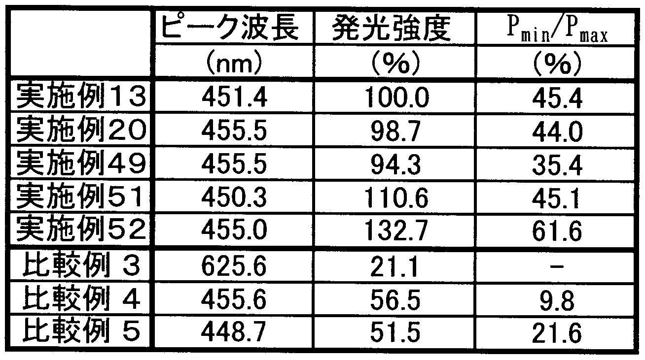
[0074] 当該実施形態によって得られた蛍光体は、 CoK a線を用いた粉末法による X線回 折パターンにおいて、ブラッグ角度(2 0 )が、 35° 力も 37° の範囲に最も強度の強 い回折ピークを示し、さらに、当該粉末法による X線回折パターンのブラッグ角度(2 0 )力 23. 6° 力ら 25. 6° 、 33° 力ら 35° 、 39.で 力ら 40.で 、43° 力ら 44 ° の範囲にそれぞれ、 2つ、 2つ、 1つ、 1つの特徴的な回折ピークが見られ、ブラッ グ角度(2 Θ )が、 35° 力も 37° の範囲に見られる最も強度の強い回折ピークの相対 強度を 100%としたとき、これらの回折ピークの相対強度は 2. 0%以上、 40%以下を 示すという特徴がある。この特徴を満たすことにより、波長 250nmカゝら 430nmの範囲 の光で励起したとき、発光スペクトルにおける最大ピーク波長が 400nmから 500nm の範囲にあるより発光効率の良 、蛍光体を得ることが可能である。
[0075] また、当該粉末法による X線回折パターンにおいて、ブラッグ角度(2 Θ )が 26° 力 ら 33° 、38. 7° 力ら 39. 7° 、42. 0° 力ら 42. 8° の範囲には、ブラッグ角度(2 0 )が 35° 力 37° の範囲に見られる最も強度の強い回折ピークの相対強度を 100 %としたとき、相対強度が 10%以上の回折ピークが無いことが好ましい。これは、上 記範囲に見られる回折ピークは波長 400nm〜500nmの範囲に発光スペクトルのピ ークを示す相とは異なる不純物相によるものであると考えられるためである。つまり、 当該不純物相が少なければ、生じた不純物相の為に励起光や蛍光体力 発生した 光が吸収されることに起因する発光効率低下を回避でき、高い発光強度が得らると 考えられるためである。
[0076] さらに、 CoK o;線を用いた粉末法による X線回折パターンにおいて、ブラッグ角度( 2 0 )が、 35° 力も 37° の範囲にある最も強度の強い回折ピークに注目すると、構成 元素に A1が含まれることによって、ピークが 2つになっていることが解る(後述の、図 2 及び図 8における、実施例 2、 4、 6、実施例 13、 20、 45、 49、 52の各蛍光体試料の X線回折パターン参照)。そして、 A1を加え、ピークが 2つになったものの方力 発光 特性が優れて 、る傾向にある。
[0077] さらに、本発明者らは上記 XRDのピーク位置の測定と伴に、前記粉末 X線測定結 果を基としてリートベルト手法を用い、蛍光体試料の結晶構造解析を行った。リートべ ルト手法とは、実際の測定力 得られた X線の実測回折強度と、その結晶構造を予 測して組み立てた結晶構造モデル力 理論的に計算で得られる X線の回折強度とを 比較し、両者の差を小さくするように、後者のモデルにおける種々の構造パラメータ を、最小二乗法により精密化することで、より正確な結晶構造のモデルを導くもので ある。リートベルト解析にはプログラム" RIETAN— 2000"を用い、参考とした結晶構 造は、 JCPDSカード 53— 0636に記載された Sr Al Si O N の結晶構造を用い
2 2 10 4 14
た。
[0078] 当該リートベルト手法による結晶構造解析の結果、蛍光体試料の発光特性の向上 には、当該蛍光体試料の a軸、 b軸、 c軸、各結晶格子の格子定数 ¾JCPDSカードに 記載された Sr Al Si O N の結晶構造よりも小さぐまた体積も小さいほど良い傾
2 2 10 4 14
向力 S見られた。一方、非特許文献 Z. Anorg. Allg. Chem. , 2004, 630, 1729 に報告のある SrSi N結晶構造と比較した場合は、当該蛍光体試料の a軸、 b軸、 c
6 8
軸、各結晶格子は SrSi N結晶構造よりも大きぐまた体積も大きいほど良い傾向が
6 8
見られた。この現象の詳細な理由は不明である力 蛍光体試料中に含まれる Si原子 と A1原子とが、または、窒素原子と酸素原子とが置き換わることにより結晶格子およ び体積が変化したと考えられる。
[0079] さらに、本発明者らは、結晶構造の結晶格子および体積は結晶構造中に含まれる A1および酸素量により関係していることから、当該蛍光体の発光効率を始めとする発 光特性は A1および酸素量が影響を与えて 、るのではな 、かと 、う観点に想到した。 そして、当該 A1および酸素量が蛍光体の結晶格子の体積を規定していることから、 発光効率の良い蛍光体を得ることが出来る結晶格子の体積があることに想到し、当 該結晶格子の体積が 345A3以上 385A3以下、さらに好ましくは体積が 353A3以上 385A3以下であることを見出した。さらに、当該 Aほたは酸素の量が蛍光体の結晶 格子の格子定数も規定して 、ることから、発光効率の良 、蛍光体を得ること出来る結 晶格子の格子定数もあることに想到し、当該格子定数が、 aは 7. 85A以上、 8. 28 A以下、 bは 9. 26A以上、 9. 58A以下、 cは 4. 80A以上、 4. 92A以下であること を見出した。(尚、本発明において、 a軸、 b軸、 c軸の採り方 ίお CPDSカードを参考 に示している。従って、原子座標の採り方により a軸、 b軸、 c軸の順が入れ替わっても 同義である。)
[0080] また、本発明者らは、蛍光体の結晶子サイズが、当該蛍光体の発光効率を始めと する発光特性に影響を与えて 、るのではな 、かと 、う観点に想到した。
そこで、本発明に係る蛍光体試料について、粉末 X線回折測定により得られた回折 パターンの複数の回折ピークについて半価幅 Bを算出し、シエラーの式 Dx=0. 9 λ /Bcos Θ (ここで、 Dxは結晶子の大きさ、 λは測定に用いた X線の波長、 Bは回折 ピークの半価幅、 Qは回折ピークのブラッグ角である。)を用いて、 2 Θ力 39. 7° か ら 40.で 、 43° 力ら 44° 、 66° 力ら 66. 5° の範囲にある 3つの回折ピーク力ら、 結晶子の大きさ (Dx)を平均化して求めた。ここで、結晶子サイズが大きいほど、作製 した蛍光体粒子の結晶性が良いことを表しており、発光効率の向上が見込まれた。 当該観点より本発明者らは、結晶子サイズが 20nm以上、好ましくは 50nm以上、さら に好ましくは 80nm以上、であれば、当該蛍光体を発光装置として用いた場合十分 な発光強度を得ることが出来ることを見い出した。
[0081] 本発明に係る蛍光体を粉体の形で用いる場合は、当該蛍光体粉体の平均粒径が 50 m以下であることが好ましい。これは、蛍光体粉体において発光は主に粒子表 面で起こると考えられるため、平均粒径(尚、本発明において平均粒径とは、中位径(
D50)のことである。)が 50 m以下であれば、粉体単位重量あたりの表面積を確保 でき輝度の低下を回避できるからである。さら〖こ、当該粉体をペースト状とし、発光体 素子等に塗布した場合にも当該粉体の密度を高めることができ、この観点からも輝度 の低下を回避することができる。また、本発明者らの検討によると、詳細な理由は不 明であるが、蛍光体粉末の発光効率の観点から、平均粒径が 1. O /z mより大きいこと が好ましいことも判明した。以上のことより、本発明に係る蛍光体粉体の平均粒径は、 1. Ο μ m以上 50 μ m以下、さらに好ましくは 5. 0 μ m以上、 30 μ m以下の粒子径で あることが好まし 、。ここで 、う平均粒子径 (D50)は、ベックマン 'コールター社製 L S230 (レーザー回折散乱法)により測定された値である。また、上記観点から、本発 明に係る蛍光体粉末の比表面積 (BET)の値は 0. 05m2Zg以上、 5. 00m2Zg以 下であることが好ましい。
[0082] 本実施形態の蛍光体は、発光スペクトルのピークを 400nm〜500nmの範囲に持 ち、ピーク形状はブロードであり、発光強度および輝度に優れているため白色 LED 照明用蛍光体としてふさわしい。さらに、近紫外'紫外の範囲に良好な励起帯を有す るため、例えば、ワンチップ型白色 LED照明として提案されている近紫外 ·紫外発光 (波長 380〜410nm付近)する LEDと、当該 LEDから発生する近紫外'紫外光によ り励起されて赤色 (R)発光する蛍光体、緑色 (G)発光する蛍光体、青色 (B)発光す る蛍光体とを組み合わせ、当該 R' G · B他の蛍光体力 得られる光の混色を利用して 白色を得る方式の白色 LED照明に使用した場合には、最高の発光強度に近い状態 で使用することが可能である。即ち、近紫外'紫外の光を発する発光部と当該蛍光体 を組み合わせることにより、高出力、演色性の良い白色光源および白色 LED照明、 さらにはこれらを使用した照明ユニットを得ることができる。
[0083] 粉末状となった本実施形態の青色蛍光体と、公知の緑色蛍光体、赤色蛍光体とを 組み合わせ、本実施形態の蛍光体を含む蛍光体混合物を作成し、波長域 250nm 力ら 450nm、好ましくは波長域 350nm力ら 430nmの!、ずれかの光を発光する発光 部と組み合わせることで、各種の照明装置や、主にディスプレイ装置用バックライト等 を製造することができる。 [0084] 組み合わせる緑色蛍光体としては、例えば SrAISi N: Ce、 Sr Al Si ON : Ce
4 7 2 2 10 14
、 SrAl Si O N : Ce (0≤x≤l)、 (Ba, Sr, Ca) Si O N: Euゝ ZnS : Cu, l +x 4-x x 7-x 2 2 2
Al、 ZnS : Cu、 SrAl O: Euゝ BAM :Eu, Mnゝ (Ba, Sr, Ca, Mg) SiO: Euゝ Sr
2 4 2 4 3
SiO: Euが挙げられる力 この限りではない。また、組み合わせる赤色蛍光体として
5
は、 Y O S :Eu、 La O S :Eu、 3. 5MgO -0. 5MgF -GeO: Mn、 (La, Mn, Sm)
2 2 2 2 2 2
O S -Ga O : Eu、 SrS :Eu、 CaS :Eu、 Sr Si N : Eu、 (Ca, Sr) Si N : Eu、 (Ba
2 2 2 3 2 5 8 2 5 8
, Sr, Ca) MgSi O : Eu, Mn、 CaAlSiN : Euが挙げられるが、この限りではない。
3 2 8 3
[0085] 発光部として、例えば、紫外から近紫外の 、ずれかの範囲で発光する LED発光素 子、紫外光を発生する放電灯を用いることができる。例えば、本実施形態の蛍光体を 含んだ蛍光体混合物を、紫外光を発生する放電灯と組み合わせることで蛍光灯や照 明ユニットやディスプレイ装置、また、紫外力 近紫外発光する LED発光素子と組み 合わせることでも、照明ユニットやディスプレイ装置を製造することができる。さらに、 本発明に係る蛍光体を、電子線を発生する装置と組み合わすことによつてもディスプ レイ装置を製造することができる。
[0086] 本実施形態の蛍光体の混合物と発光部との組み合わせの方法は、公知の方法で 行っても良いが、発光部に LEDを用いた発光装置の場合は、下記のようにして発光 装置を作製することが出来る。以下、図面を参照しながら、発光部に LEDを用いた発 光装置について説明する。
[0087] 図 15 (A)〜(C)は、砲弾型 LED発光装置の模式的な断面図であり、図 16 (A)〜( E)は、反射型 LED発光装置の模式的な断面図である。尚、各図面において、相当 する部分については同様の符号を付し、説明を省略する場合がある。
[0088] まず、図 15 (A)を用いて、発光部に LEDを用い、前記蛍光体混合物と組み合わせ た発光装置の 1例について説明する。砲弾型 LED発光装置においては、リードフレ ーム 3の先端に設けられたカップ状の容器 5内に、 LED発光素子 2が設置され、これ らが透光性の榭脂 4にてモールドされている。当該実施の形態では、前記蛍光体混 合物または前記蛍光体混合物をシリコンやエポキシ等の透光性のある樹脂に分散さ せた混合物(以下、混合物 1と記載する。)を、カップ状の容器 5内の全てに埋め込む ものである。榭脂中に SiOや Al Oなどの光の分散材を含有させる構成も好ましい。
2 2 3 [0089] 次に、図 15 (B)を用いて、異なる発光装置の 1例について説明する。当該実施の 形態では、混合物 1をカップ状の容器 5上および LED発光素子 2上面に塗布したも のである。
次に、図 15 (C)を用いて、さらに異なる発光装置の 1例について説明する。当該実 施の形態では、蛍光体混合物 1を LED発光素子 2の上部に設置したものである。
[0090] 以上、図 15 (A)〜(C)を用いて説明した砲弾型 LED発光装置は、 LED発光素子 2からの光の放出方向は上方向である力 光の放出方向が下方向でも同様の方法で 発光装置の作成は可能である。例えば、当該 LED発光素子 2の光の放出方向に反 射面、反射板を設け、同発光素子 2から放出される光を反射面に反射させて外部に 発光させるのが反射型 LED発光装置である。そこで、図 16 (A)〜(E)を用い、反射 型 LED発光装置と本実施形態の蛍光体混合物とを、組み合わせた発光装置の例に ついて説明する。
[0091] まず、図 16 (A)を用いて、発光部に反射型 LED発光装置を用い、本実施形態の 蛍光体混合物と組み合わせた発光装置の 1例について説明する。反射型 LED発光 装置においては、片方のリードフレーム 3の先端に LED発光素子 2が設置され、この LED発光素子 2からの発光は、下方に向かい反射面 8により反射されて上方より放 出される。当該実施の形態では、混合物 1を反射面 8上に塗布するものである。尚、 反射面 8が形成する凹部内には、 LED発光素子 2を保護するため透明モールド材 9 が充填される場合もある。
次に、図 16 (B)を用いて、異なる発光装置の 1例について説明する。当該実施の 形態では、混合物 1を LED発光素子 2の下部に設置したものである。
次に、図 16 (C)を用いて、異なる発光装置の 1例について説明する。当該実施の 形態では、混合物 1を、反射面 8が形成する凹部内に充填したものである。
次に、図 16 (D)を用いて、異なる発光装置の 1例について説明する。当該実施の 形態では、混合物 1を、 LED発光素子 2を保護するための前記透明モールド材 9の 上部に塗布したものである。
次に、図 16 (E)を用いて、異なる発光装置の 1例について説明する。当該実施の 形態では、混合物 1を、 LED発光素子 2の表面に塗布したものである。 砲弾型 LED発光装置と反射型 LED発光装置とは、用途に応じて使い分ければよ いが、反射型 LED発光装置には、薄くできる、光の発光面積を大きくできる、光の利 用効率を高められる等のメリットがある。
[0092] 以上説明した発光装置を高演色性照明用光源として使用する場合には、演色性に 優れる発光スペクトルを有していることが必要であるので、 JIS Z 8726の評価方法 を用いて、本実施形態の蛍光体を含む蛍光体混合物を組み込んだ発光装置の演色 性を評価した。 JIS Z 8726の評価において、当該光源の平均演色評価数 Raが 80 以上であれば、優れた発光装置といえる。そして、好ましくは、日本人女性の肌色の 成分を示す指標である特殊演色評価数 R15が 80以上であれば、非常に優れた発光 装置といえる。ただし、演色性を求めない用途や異なる目的によっては上記指標を 満たさなくても良い。そこで、波長 250nmから 430nmの範囲のいずれかの発光をお こなう発光部からの光が本実施形態の蛍光体を含む蛍光体混合物へ照射され、当 該蛍光体混合物が発光をおこなう発光装置を作製した。尚、発光部としては 405nm に発光する紫外 LEDを用いた。その結果、本発明に係る蛍光体を混合することで、 当該発光装置の相関色温度を 10000Kから 2000K (さらに好ましくは、 7000K力 2500K)の範囲としたとき、当該発光装置の平均演色評価数 Raが 80以上、さらに好 ましいことに R15が 80以上、 R9が 60以上を有する演色性に優れた発光装置となつ た。即ち、当該発光装置は、高輝度で非常に演色性に優れた光源であることが判明 した。
[0093] 一方、本実施形態に係る蛍光体混合物を榭脂中等に分散させ、蛍光体シートとす る構成も好ましい。
当該蛍光体シートを製造する際に用いられる媒体となる材料としては、エポキシ榭 脂、シリコン榭脂、を始めとする各種の榭脂、または、ガラス等が考えられる。当該蛍 光体シートの使用例としては、当該蛍光体シートと適宜な発光を行う光源とを組み合 わせ、所定の発光を行うことが可能である。なお、当該蛍光体シートを励起する励起 光は、波長 250nmから 430nmの光であれば良ぐ LED等の発光素子を始めとして 、 Hg放電による紫外線光源、レーザーによる光源等でもよい。
[0094] 次に、本実施形態に係る蛍光体の製造方法について、 SrAl Si O N : Eu ( x 6-x 1 + x 8-x 但し、 x=0. 8、 Eu/ (Sr+Eu) =0. 030である。)の製造を例として説明する。 尚、蛍光体原料の焼成時における蒸発のため、原料の仕込み組成と、焼成後の生 成した組成とが異なる。特に、 1700°C以上の焼成および長時間の焼成においては、 Si Nが当該焼成によって次第に昇華していくため、狙いのモル比より多めに仕込ん
3 4
でおいた方が好ましい。ただし、昇華量は焼成時の条件により変化するため、仕込み 量は、各々の焼成条件によって調整することが好ましい。そこで以下の説明において は、便宜上、蛍光体原料の配合比率より算定した組成式を示している。従って、本実 施形態では蛍光体を、原料の仕込み時の組成式 SrAISi O N : Euを以て標
6. 5 1. 25 9. 50
記し、製造方法について説明する。ここで、 zZ (m+z)と EuZ (Sr+Eu)とは同じ意 味である。尚、仕込み時において付活剤元素の原料中に含まれる酸素量は少量の ため無視している。
[0095] 一般的に蛍光体は固相反応により製造されるものが多ぐ本実施形態の蛍光体の 製造方法も固相反応によって得ることができる。しかし、製造方法はこれらに限定され るものではない。 M元素、 A元素、 B元素の各原料は窒化物、酸化物、炭酸塩、水酸 化物、塩基性炭酸塩などの市販されている原料でよいが、純度は高い方が好ましい ことから、好ましくは 2N以上、さらに好ましくは 3N以上のものを準備する。各原料粒 子の粒径は、一般的には、反応を促進させる観点力 微粒子の方が好ましいが、原 料の粒径、形状により、得られる蛍光体の粒径、形状も変化する。このため、最終的 に得られる蛍光体に求められる粒径や形状に合わせて、近似の粒径を有する窒化 物等の原料を準備すればよいが、好ましくは 50 m以下の粒子径、さらに好ましくは 0. 以上 10. 0 m以下の粒子径の原料を用いると良い。 Z元素も原料は巿販 の窒化物、酸化物、炭酸塩、水酸化物、塩基性炭酸塩、もしくは単体金属が好ましい 。勿論、各原料の純度は高い方が好ましぐ 2N以上、さらに好ましくは 3N以上のも のを準備する。特に、 M元素の原料として炭酸塩を使用した場合には、本実施形態 の蛍光体の構成元素に含まれない元素力もなる化合物を、フラックス (反応促進剤) として添加することなぐフラックス効果を得ることができるため好ま 、構成である。
[0096] 組成式 SrAl Si O N : Euの製造であれば、焼成後の各元素のモル比が S
0. 8 5. 2 1. 8 7. 2
r:Al: Si: O :Eu=0. 970 : 0. 8 : 5. 2 : 1. 8 : 0. 030となるように、焼成時の原料糸且 成の減少分を調整し仕込み組成を決めればよい。ここでは、仕込み組成式 SrAISi
6.
O N : Eu (但し、 Eu/ (Sr+Eu) 0· 030)として製造した。各元素の原料と
5 1. 25 9. 50
して例えば、 Μ元素、 Α元素、 Β元素の原料として、それぞれ SrCO (3N) , Al O (3
3 2 3
N)、 A1N (3N)、 Si N (3N)を準備し、 Z元素としては、 Eu O (3N)を準備するとよ
3 4 2 3
い。これらの原料をそれぞれ、 SrCOを 0· 970mol、 Al Oを 0· 25/3 mol、 A1N
3 2 3
を(1. 0-0. 25/3 X 2) mol、 Si Nを 6. 5/3mol、 Eu Oを 0. 030/2mol秤量
3 4 2 3
し混合する。 Sr原料として炭酸塩を使用したのは、酸ィ匕物原料は融点が高くフラック ス効果が期待できないのに対し、炭酸塩など低融点の原料を使用した際には、原料 自体がフラックスとして働き、反応が促進され、発光特性が向上するためである。なお 、原料中にわず力な C (炭素)を添加し、焼成時に還元性を高めても良い、ただし焼 成後の試料に Cの濃度が多く残ると、発光特性を低下させるため、焼成後の試料に 含まれる Cの濃度は 0. 1重量%以下になるように調整する必要がある。また、原料と して酸化物を使用した場合、フラックス効果を得るために、フラックスとして別の物質 を添加してもよいが、その場合には当該フラックスが不純物となり、蛍光体の特性を 悪ィ匕させる可能性があることに注意する必要がある。
[0097] 当該秤量 ·混合については、大気中で行っても良いが、各原料元素の窒化物が水 分の影響を受けやす 、ため、水分を十分取り除 、た不活性雰囲気下のグローブボッ タス内での操作が便宜である。混合方式は湿式、乾式どちらでも構わないが、湿式混 合の溶媒として水を用いると原料が分解するため、適当な有機溶媒または液体窒素 を選定する必要がある。装置としてはボールミルや乳鉢等を用いる通常のものでょ ヽ 。尚、当該フラックス効果については、実施例においても説明する。
[0098] 混合が完了した原料をるつぼに入れ、焼成炉内に雰囲気ガスを流通させながら 16 00°C以上、より好ましくは 1700°C以上 2000°C以下で 30分間以上保持して焼成す る。焼成温度が 1600°C以上であれば、固相反応が良好に進行して発光特性に優れ た蛍光体を得ることが可能となる。また 2000°C以下で焼成すれば、過剰な焼結や、 融解が起こることを防止できる。尚、焼成温度が高いほど固相反応が迅速に進むた め、保持時間を短縮出来る。一方、焼成温度が低い場合でも、当該温度を長時間保 持することにより目的の発光特性を得ることが出来る。しかし、焼成時間が長いほど粒 子成長が進み、粒子形状が大きくなるため、 目的とする粒子サイズに応じて焼成時 間を設定すればよい。
[0099] 焼成炉内に流通させる雰囲気ガスとしては、窒素に限らず、希ガス等の不活性ガス 、アンモニア、アンモニアと窒素との混合ガス、または窒素と水素との混合ガスのいず れかを用いると良い。但し、当該雰囲気ガス中に酸素が含有されていると蛍光体粒 子の酸ィ匕反応が起こるため、不純物として含まれる酸素はできるだけ少なぐ例えば lOOppm以下であることが好まし 、。さらに雰囲気ガス中に水分が含有されて!、ると 、酸素と同様、焼成時に蛍光体粒子の酸ィ匕反応が起こるため、不純物として含まれる 水分もできるだけ少なぐ例えば lOOppm以下であることが好ましい。ここで、雰囲気 ガスとして単一ガスを用いる場合は窒素ガスが好まし 、。アンモニアガスの単独使用 による焼成も可能である力 窒素ガスに比べアンモニアガスはコスト的に高いことや、 腐食性ガスであることのため、装置および低温時の排気方法に特別な処置が必要と なるので、アンモニアを用いる場合には、窒素との混合ガスとするなど、アンモニアを 低濃度にして用いる方が好ましい。例えば、窒素ガスとアンモニアの混合ガスを用い る場合、窒素は 80%以上、アンモニアは 20%以下とすることが好ましい。また、窒素 と他のガスとの混合ガスを用いる場合も、窒素以外のガス濃度が高まると、雰囲気ガ ス中の窒素の分圧が低くなるので、蛍光体の窒化反応を促進する観点からは、 80% 以上の窒素を含む不活性または還元性ガスを用いると良 、。
[0100] さらに、当該焼成中に上述した雰囲気ガスを、例えば、 0. lmlZmin以上流量させ る状態を設けることが好ましい。これは、蛍光体原料の焼成中には当該原料力もガス が発生する力 上述の窒素、希ガス等の不活性ガス、アンモニア、アンモニアと窒素 との混合ガス、または窒素と水素との混合ガスカゝら選択される 1種類以上のガスを含 んだ雰囲気を流動(フロー)させることにより、原料力 発生したガスが炉内に充満し て反応に影響を与えることを防止でき、この結果、蛍光体の発光特性の低下を防止 できるからである。特に、蛍光体原料として炭酸塩、水酸化物、塩基性炭酸塩など、 高温で酸ィ匕物に分解する原料を使用した際には、ガスの発生量が多いため、焼成炉 内にガスを流通させ、発生したガスを排気させる構成を採ることが好ま ヽ。
[0101] 一方、蛍光体製造における蛍光体原料焼成の段階において、焼成炉内の圧力は 、炉内に大気中の酸素が混入しないよう加圧状態であることが好ましい。ただし、該 加圧が 1. OMPa (本発明において、炉内圧力とは大気圧力 の加圧分の意味である 。)を超えると炉設備の設計上、特殊な耐圧設計が必要となることから、生産性を考慮 すると該加圧は 1. OMPa以下であることが好ましい。また、該加圧が高くなると、蛍光 体粒子間の焼結が進み過ぎ、焼成後の粉砕が困難となることがあるため、当該焼成 中の炉内圧力は 1. OMPa以下が好ましぐ更に好ましくは 0. OOlMPa以上、 0. 1 MPa以下であることが好まし 、。
[0102] 尚、るつぼとしては Al Oるつぼ、 Si Nるつぼ、 A1Nるつぼ、サイアロンるつぼ、 C (
2 3 3 4
カーボン)るつぼ、 BN (窒化ホウ素)るつぼなどの、上述したガス雰囲気中で使用可 能なものを用いれば良いが、なかでも、窒化物からなるるつぼが好ましぐ特に BNる つぼを用いると、るつぼ力 の不純物混入を回避することができ好ましい。焼成後に 含まれる不純物量としては、 B (ホウ素)および Zまたは Cが 0. 1重量%以下であれば 、発光特性を阻害することなく好ましい。
[0103] 焼成が完了した後、焼成物をるつぼから取り出し、乳鉢、ボールミル等の粉砕手段 を用いて、所定の平均粒径となるように粉砕し、組成式 SrAl Si O N : EiTC
0. 8 5. 2 1. 8 7. 2 示される蛍光体を製造することができる。得られた蛍光体はこの後、必要に応じて、 洗浄、分級、表面処理、熱処理を行う。洗浄方法としてはフッ酸、塩酸、硫酸、硝酸な どを用いた酸性溶液中での洗浄が、粒子表面に付着した Fe等の金属原子や、未反 応で残留した原料粒子を溶解するため好ましい。ここで、得られた蛍光体に含まれる Fe、 Ni、 Coの量は lOOppm以下であることが好ましい。
[0104] M元素、 A元素、 B元素、 Z元素として、他の元素を用いた場合、および付活剤であ る Z元素の付活量を変更した場合も、各原料の仕込み時の配合量を所定の組成比 に合わせることで、上述したものと同様の製造方法により蛍光体を製造することができ る。ただし、焼成条件によっては、焼成時に原料の蒸発、昇華等が起こるため、その 分の原料の仕込み組成を考慮した原料の混合 ·焼成を行う。
実施例
[0105] 以下、実施例に基づいて、本発明をより具体的に説明する。
(実施例 1から 6、および、比較例 1、 2) 実施例 1から 6では、本発明に係る原料の仕込み組成式 SrAISi ON: Eu(Eu/( b n
Sr+Eu) =0.030、 n=2/3m+a+4/3b-2/3o, m=l、 a=l、 o=l)で示さ れる蛍光体において、 Sr、 Al、 Oのモル比をそれぞれ 1、 1、 1に固定し、 bZm比を 変えた試料を調製し、当該試料の発光特性、および構造について検討した。
まず、以下の手順により実施例 1に係る試料を製造した。
SrCO (3N)、 A1N(3N)、 Si N (3N)、EuO (3N)を準備し、各元素のモル比
3 3 4 2 3
力 Sr:Al:Si:Eu=0.970:1:4:0.030となるように各原料を、 SrCOを 0.970mo
3
1、 A1Nを lmol、 Si Nを 4Z3mol、 Eu Oを 0.030Z2mol秤量し、大気中にて乳
3 4 2 3
鉢を用いて混合した。 SrCOについては焼成時に分解し SrOとなるため、酸素の量
3
の計算では SrOとして計算した。混合した原料を BNるつぼに入れ、炉内を一度真空 引きした後、流通する窒素雰囲気中(フロー状態、 20. OLZmin)、炉内圧 0.05M Paで 1800°Cまで 15°CZminで昇温し、 1800°Cで 3時間保持 '焼成した後、 1800 °Cから 50°Cまで 1時間 30分間で冷却した。その後、焼成試料を大気中にて適当な 粒径になるまで乳鉢を用いて解砕し、 b/m=4.0である実施例 1に係る蛍光体試料 を得た。尚、当該組成式は、使用した原料の配合比率より算定した組成である。従つ て、焼成時に Siの昇華や酸素の減少が起こるため、焼成後の蛍光体生成物におい ては、原料の配合比率 (仕込み組成比)よりも Siや酸素の少な 、組成となって 、ると 考えられる。
[0106] 次に、当該 bZm比を、 bZm=5(実施例 2)、 bZm=6(実施例 3)、 bZm=7(実 施例 4)、 bZm=8 (実施例 5)、 bZm=9 (実施例 6)となるように、各原料の混合比 を調整した以外は、実施例 1と同様にして実施例 2から 6に係る蛍光体試料を製造し た。
[0107] また、当該 bZm比を、 bZm=2(比較例 1)、 bZm=3(比較例 2)となるように混合 比を調整した以外は、実施例 1と同様にして比較例 1、 2に係る蛍光体試料を製造し た。
[0108] 製造した実施例 1から 6、比較例 1、 2に係る試料について、発光のピーク波長およ び発光強度を測定した。当該測定結果を表 1、図 1に示す。
ここで、実施例 1から 6、比較例 1、 2においては、発光のピーク波長とは、ある波長 の光またはエネルギーを蛍光体に照射した際、当該蛍光体力 放出される光のスぺ タトルの最大ピークが示す波長のことであり、発光強度とは、当該発光のピーク波長 における強度のことである。なお、発光スペクトル、および後に示す励起スペクトルの 測定には日本分光 (株)社製分光蛍光光度計 FP— 6500を用いて測定した。
実施例 1から 6、比較例 1 2においては、励起光として波長 405nmの光を蛍光体 に照射した。そして、 bZm= 7 (実施例 4)のピーク波長における発光強度の値を 10
0%と規格ィ匕して、各実施例の発光強度を示した。
図 1は、縦軸に当該蛍光体試料の発光強度の相対強度をとり、横軸には bZm比の 値をとつたグラフである。
次に、実施例 2 4 6、および比較例 2に係る試料に対し粉末法による X線回折パ ターンを測定した。さらに、実施例 4に係る試料に対しリートベルト解析を行った。当 該結果を図 2に示す。図 2には、上から、比較例 2、実施例 2 4 6、実施例 4のリート ベルト解析結果、 JCPDSカード(53— 0636)の回折パターンの順で X線回折パター ンを示した。
[0109] 表 1、図 1の結果から明らかなように、実施例 1から 6に係る蛍光体の発光強度は、 b Zm比の値が大きくなるにつれ強くなり、 bZm=6から bZm= 7付近で最も強い発 光強度を示した。
また、比較例 1 2に係る b/m比の値が 3以下の試料は、波長 400nm 500nmの 範囲に、発光スペクトルのピークが見られず、波長 630nm付近に発光スペクトルのピ ークを持つ橙色蛍光体であった。
[0110] [表 1]
Figure imgf000029_0001
ここで、図 2の粉末法による X線回折パターンの測定方法について説明する。
測定する蛍光体は、焼成後に乳鉢、ボールミル等の粉砕手段を用いて所定 (好まし くは 1. 0 m〜50. 0 m)の平均粒径となるように粉砕し、材質がチタン製のホルダ 一に平らになるように詰め、 XRD装置 理学電気株式会社製「RINT 2000」にて測 定を行った。
測定条件を下記に示す。
使用測定機:理学電気株式会社製「RINT 2000」
X線管球: CoK o;
管電圧: 40kV
管電流: 30mA
スキャン方法: 2 0 / 0
スキャン速度: 0. 3° Zmin
サンプリング間隔: 0. 01°
スタート角度(2 Θ ) : 10°
ストップ角度(2 Θ ) : 90°
[0112] また、ブラッグ角度(2 0 )のズレについては、 X線が照射される試料面が平らでない こと、 X線の測定条件、特にスキャンスピードの違いなどにより生じていると考えられる 。そのため、特徴的な回折ピークが見られる範囲も若干のズレが起きることは許容さ れると考えられる。当該ズレをなるベく抑えるために、スキャンスピードを 0. 3° /min とした上で、蛍光体試料中に Siを混ぜ、 X線の測定後に Siピークのズレを補正するこ とにより、ブラッグ角度(2 Θ )および面間隔 d (A)を求めている。以下、後述する、図 8 に示す実施例 13、 20、 45、 49、 52に係る試料、および図 13に示す実施例 45、比 較例 3に係る試料についても同様に測定を行った。
[0113] 図 2の粉末法による X線回折パターンの結果から明らかなように、強い発光強度を 示す実施例 4と波長 400ηπ!〜 500nmの範囲に発光ピークを有さな!/、比較例 2、実 施例 4よりも発光ピークの小さな実施例 2、 6との回折パターンを比較してみる。すると 、比較例 2および実施例 2、 6においては、実施例 4で回折ピークが見られないブラッ グ角度(2 Θ )に多くの回折ピークを確認することができ、特にブラッグ角度(2 Θ )が 2 6° 〜33° 、38. 7° 〜42. 8° の範囲において回折ピークを確認することができた 。さらに、比較例 2の回折パターンには、実施例 4と同様の回折パターンも見られるが 、その生成割合は、全蛍光体生成相の 40%程度であり、黄色蛍光体と考えられる他 の生成相が多く含まれていることが判明した。
即ち、ブラッグ角度(2 0 )が 26° 〜33° 、38. 7° 〜42. 8の範囲にある回折ピー クは、波長 400ηπ!〜 500nmの範囲に発光スペクトルのピークを示す相とは異なる相 (不純物相)に起因するものであると考えられる。従って、波長 400ηπ!〜 500nmの範 囲に発光スペクトルのピークを持ち、発光強度の強い蛍光体を得るには、上記生成 相(SrAI Si O N と同様な相)を 50%以上含み、これらの不純物相が示す回
6 1 8
折ピークを有しな 、蛍光体であることが好ま 、。
[0114] さらに図 2には、 JCPDSカード(53— 0636)で報告されている Sr Al Si O N の
2 2 10 4 14 結晶構造を基にシミュレートした回折パターンと、 Sr Al Si O N
2 2 10 4 14と結晶構造を基 に、実施例 4の X線回折パターンをリートベルト解析して求めたシミュレーション結果 を示している。リートベルト法とは実施に測定して得られた実測回折強度と、その結晶 構造を予測して組み立てた結晶構造モデルから、理論的に計算で得られる回折強 度を比較し、両方の差を小さくするように後者のモデルにおける種々の構造パラメ一 タを最小二乗法により精密化して、より正確な結晶構造を導くものである。
[0115] 】じ?03カード(53— 0636)、にて報告されてぃる3 八1 31 O N の結晶構造は
2 2 10 4 14
空間群 Imm2で示される斜方晶系であり、格子定数は a = 8. 279A、b = 9. 576A 、 c=4. 916Aと報告されている。ここで、実施例 4の解析結果によると、結晶構造は 同様に斜方晶系である力 S、格子定数 ίま a= 7. 902A, b = 9. 278A, c=4. 838A となり、結晶単位格子は、 JCPDSカードが従来報告しているものよりも非常に小さい 結果となっていた。実施例 3、 5、 6においても全て同様の結果であった。実施例 4〜 6において、格子定数力JCPDSカードの値よりも小さくなつた理由は、 SrAl Si O N の組成式で示される当該蛍光体生成相において、 Xの値が 1以下の組成をと 8
つているか、または、 x= lであっても酸素原子が欠損した組成をとっている為、格子 が縮んで!/ヽるものと考えられる。
[0116] 一方、非特許文献 Z. Anorg. Allg. Chem. , 2004, 630, 1729に報告のある Sr Si N結晶構造は、上言 6JCPDSカードに記載された Sr Al Si O N 結晶同様の
6 8 2 2 10 4 14
斜方晶系の結晶を有しているが、 A1原子および酸素原子が少ないことによって、格 子定数は a= 7. 855A、b = 9. 26θΑ、 c=4. 801 Aと報告されており、本実施例 で得られた蛍光体よりもさらに小さな格子定数を有している。
[0117] 以上のことから、本発明者らは本発明に係る蛍光体が、 JCPDSカードに記載され た Sr Al Si O N および Z. Anorg. Allg. Chem. , 2004, 630, 1729 に記載
2 2 10 4 14
された SrSi Nの結晶構造と同様の類似してはいるものの、 Aほたは酸素原子の存
6 8
在量を変化させたことで、結晶面間隔の異なる新規な結晶構造を有し SrAl Si O N で示される組成式を有する新規な蛍光体であることに想到した。よって、発光
+ x 8-X
効率の良い蛍光体を得るためには、結晶格子の体積力 Sr Al Si O N の結晶構
2 2 10 4 14 造と SrSi Nの結晶構造との間にあること。即ち、結晶体積が 345A3以上、 385A3
6 8
以下であること。さらに好ましくは各結晶格子の格子定数が、 aは 7. 85 A以上、 8. 2 8A以下、 bは 9. 26A以上、 9. 58A以下、 cは 4. 80A以上、 4. 92A以下であれ ば良い。また、 Xの範囲としては 0≤x≤2であり、より格子定数および単位格子の小さ な 0≤χ≤1. 0が好ましい。
[0118] また、実施例 4の解析結果より、発光強度の強い蛍光体を得るには、解析結果から 得られた回折ノターンに近く、 26° 力ら 33° 、 38. 7° 力ら 39. 7° 、 42. 0° 力ら 4 2. 8° にみられる不純物相の回折ピークがないことが良いことが判明した。これは、 原料の混合段階や焼成条件において、目的とする組成よりも Si Nまたは A1N原料
3 4
が過剰に存在すると、これらが、わずかであるが不純物相となり回折ピークとして現れ てくる為であると考えられる。したがって、各焼成条件にあった原料の混合比などを調 整することにより、これら不純物相を低減することが可能である。上記不純物ピークは 35° 力も 37° の範囲に見られる最も強度の強い回折ピークの相対強度を 100%と したとき、 10. 0%以下で有ることが好ましい。
[0119] つまり、本発明に係る試料において、 bZm=6から bZm= 7付近で最も強い発光 強度を示すのは、 bZm=6、 bZm= 7付近の bZm比であれば、波長 400nm〜50 Onmの範囲に発光スペクトルのピークを示す組成式 SrAl Si O N で示され x 6-x 1+ x 8-x る相の割合を 50%以上の含む形で生成させることができ、当該 bZm比が bZm=6 、 bZm= 7から大きく外れてしまって不純物相が生成されてしまうのを回避できるた めであると考えられる。実際に焼成後の試料を観察すると、 bZm=6、 bZm= 7の 試料は全体がほぼ白色である力 それ以外の試料は黄色や橙色の不純物相を確認 することができる。(励起光として 405 nmの光を当てた場合、白色の部分が青色に 発光し、黄色、橙色の部分はそれぞれ黄色、橙色に発光する。)しかし、注意しなけ ればならないのは、組成式が SrAl Si O N で示されることから理解できるよう
X 6-x 1 +x 8-x
に、 bZm比の値力 常に bZm=6から bZm= 7にあることが適正なわけではなぐ a Zm比が変化すると、 bZm比の適正値も若干変化すると考えられることである。これ は、当該蛍光体は [SiN ]がネットワークを組んだ構造を基本としており、 A1はその Si
4
の一部のサイトを置換していると考えられるためである。そのため、 A1による置換量が 変化した場合、 Si量も若干変化させて、発光に適した構造をとるようにすることが好ま しい。具体的には、上記構造式に即し、変化した A1の置換量に対応して Siの量を変 化させ、発光に適した構造を取るようにすればよい。
[0120] また、解析結果から推定される蛍光体生成相の組成と、原料の仕込み組成との Si の比率は異なっている。これは、上述したように原料とした Si N力 1700°C付近か
3 4
ら蒸発または分解を起こすため、焼成時に Siが減少し、組成比がズレる為であると考 えられる。ここで、焼成時の焼成温度、焼成時間、焼成圧力などの条件により、 Siまた は他の元素の減少量は異なるため、目的の生成物を得るには、各焼成条件に適した 原料の仕込の量を予め調整すればょ 、。
[0121] (実施例 7から 15、および、実施例 16から 24)
実施例 7から 24では、原料秤量 '混合時の Siの仕込み組成と酸素量とを変化させ、 強い発光強度を有する蛍光体を得る為の仕込み組成および目的組成を検討した。 まず、実施例 7から 15は、実施例 1から 6で最も優れた発光強度を示した bZm= 7 (実施例 4)の試料について、今度は、 oZm比を変化させた場合の発光強度につい て検討したものである。
[0122] 実施例 7から 15を以下の手順により製造した。
原料として市販の Sr N (2N)、 SrCO (3N)、 Al O (3N)、 A1N (3N)、 Si N (3
3 2 3 2 3 3 4
N)、 Eu O (3N)を準備し、原料仕込みの組成 SrAISi O N: Eu (Eu/ (Sr+Eu
2 3 7. 0 o n
) =0. 030、 n= 2/3m+a+4/3b- 2/3o, m= l、 a= l、 b = 7)で示される蛍 光体において、 Sr、 Al、 Siのモル比を、それぞれ 1、 1、 7に固定し、 oZm比を oZm =0 (実施例 7)とした以外は、実施例 1と同様にして蛍光体試料を製造した。同様に 、 o/m=0. 50 (実施例 8)、 oZm=0. 75 (実施例 9)、 oZm= 1. 00 (実施例 10) 、oZm= l. 25 (実施例 11)、 oZm= l. 50 (実施例12)、0 !11= 1. 75 (実施例 1 3)、oZm= 2. 00 (実施例14)、0 !11= 2. 50 (実施例 15)の各試料を製造した。
[0123] 製造した実施例 7から 15に係る試料についてピーク波長、発光強度を測定した。当 該測定結果について表 2、図 3に示す。ここで、図 3は縦軸に当該蛍光体試料の発光 強度の相対強度をとり、横軸には oZm比の値をとつている。尚、発光強度において は、 oZm= l. 75 (実施例 13)のピーク波長における発光強度の値を 100%と規格 ィ匕した。尚、励起光として波長 405nmの光を用いた。
表 2、図 3の結果から明らかなように、当該各蛍光体の発光強度は、 oZm比の値が 大きくなるにつれ強くなり、 o/m= l. 75付近で最も強い発光強度を示した。
[0124] 上述したように、実施例 7から 15は、実施例 1から 6で最も優れた発光強度を示した b/m = 7 (実施例 4)の試料にっ 、て、 oZm比を変化させた場合の発光強度にっ ヽ て調査をした結果である。 bZm比だけでなぐさらに oZm比も最適化することにより 、優れた発光強度を示す蛍光体が得られることが解った。実施例 1から 6では、 b/m = 7、 o/m= lの試料において最も優れた発光強度を示した力 この実施例 7から 1 5では、 bZm= 7、 o/m= l. 75とすることで、さらに約 20%発光強度が改善するこ とが判明した。この理由としては、 SrAl Si O N で示される組成式から分かる
X 6-x 1 + x 8-x
ように、 Siのサイトの一部を、 +IV価の SUりイオン半径の大きな +ΙΠ価の A1により置 換することで、電荷のバランスが崩れると共に結晶構造が歪んでしまうと考えられるが
、その歪みを緩和するため、—III価である Nのサイトの一部を、 Nよりイオン半径の小 さな II価である Oに置換することで電荷のバランスが保たれ、発光に適した結晶構 造となるものと考えられる。したがって、 A1や Siの比率によって Oの適正量が変化す ると考免られる。
[0125] [表 2] 原料仕込み量 /mol ピーク波長 発光強度 o/m Sr3N2 SrC03 AIN Al203 Si3N4 Eu203 (nm) (%) 実施例 7 0.00 0.323 - 1.000 - 2.333 0.015 460.9 11.9 実施例 8 0.500 0.157 0.500 1.000 - 2.333 0.015 459.9 44.9 実施例 9 0.750 0.073 0.750 1.000 - 2.333 0.015 458.2 58.4 実施例 1C 1.000 一 0.970 1.000 - 2.333 0.015 459.9 63.1 実施例 11 1.250 - 0.970 0.833 0.083 2.333 0.015 456.0 77.4 実施例 12 1.500 - 0.970 0.667 0.167 2.333 0.015 453.0 90.5 実施例 13 1.750 - 0.970 0.500 0.250 2.333 0.015 451.4 100.0 実施例 14 2.000 - 0.970 0.333 0.333 2.333 0.015 449.1 94.3 実施例 15 2.500 - 0.970 0.000 0.500 2.333 0.015 451.4 19.7
[0126] 次に、実施例 16から 24は、上述した実施例 7から 15において設定した bZm=7を 、bZm=6.5に変更して検討したものである。
まず、実施例 16から 24を以下の手順により製造した。
原料仕込み組成式 SrAISi O N : Eu(Eu/(Sr+Eu) =0.030、 n=2/3m+
6.5 o n
a+4/3b— 2/3o、 m=l、 a=l、 b = 6.5)で示される 光体【こお!ヽて、 Sr、 Al、 S iのモル比を、それぞれ 1、 1、 6.5に固定し、 oZm=0(実施例 16)とした以外は、実 施例 1と同様にして蛍光体試料を製造した。同様に、 oZm=0.50(実施例 17)、o /m=0.75(実施例 18)、 oZm=l.00(実施例19)、0 !11=1.25(実施例 20) 、oZm=l.50(実施例 21)、 oZm=l.75 (実施例 22)、 oZm=2.00(実施例 2 3)、 o/m=2.50 (実施例 24)の各試料を製造した。
[0127] 製造した実施例 16から 24に係る試料についてピーク波長、発光強度を測定した。
当該測定結果について表 3、図 4に示す。ここで、図 4は縦軸に当該蛍光体試料の発 光強度の相対強度をとり、横軸には oZm比の値をとつている。尚、発光強度におい ては、 o/m=l.25 (実施例 20)のピーク波長における発光強度の値を 100%と規 格ィ匕した。尚、励起光として波長 405nmの光を用いた。
表 3、図 4の結果から明らかなように、当該各蛍光体の発光強度は、 oZm比の値が 大きくなるにつれ強くなり、 oZm=l.00から oZm=l.75付近で最も強い発光強 度を示した。
[0128] 実施例 16から 24は、実施例 7から 15の組成式における bZm比を、 bZm=7から b/m=6.5に変更したものである力 表 3、図 4の結果から、実施例 16から 24の結 果と同様、 bZm比を変化させると最適な oZm比も変化してしまうということが解る。 つまり、実施例 7力も 15にも記したように、 SrAl Si O N の構造式に即した Al x 6-x 1+x 8-x 、 Si、 0、 Nのパランスをとることが重要である。また、仕込み組成時の酸素濃度の増 加により試料の融点が低下し、それが試料の、固相反応の促進および結晶性の向上 に働 、て 、ると考えられ、焼成時の焼成温度の低下や焼成時間の短縮にも利用でき ると考えられる。
[0129] [表 3]
Figure imgf000036_0001
[0130] (実施例 25から 30)
実施例 25から 30では、 aZm比の値を変化させ、強い発光強度を有する蛍光体を 得る為の仕込み組成および目的組成を検討した。
即ち、原料仕込みの組成 SrAl Si ON : Eu (Eu/ (Sr+Eu) =0. 030、 n= 2/ a 6. 5 n
3m+a+4/3b— 2/3o、 m= l、 o= l、 b = 6. 5)で示される 光体【こお ヽて、 Sr 、 Siゝ Oのモ /kttを、それぞれ 1、 6. 5、 1に固定し、 a/mitを 0. 5力ら 2. 0の範囲で 設定した試料を混合 '焼成し、発光強度を測定した。 (b/m=6. 5、 o/m= l. 0) [0131] まず、実施例 25から 30を以下の手順により製造した。各試料の製造においては、 原料として市販の SrCO (3N)、 Al O (3N)、 A1N (3N)、 Si N (3N)、 Eu O (3N
3 2 3 3 4 2 3
)を準備し、各原料を所定の aZm比となるように各原料の混合比を調整した以外は、 実施例 1と同様にして蛍光体試料を製造した。但し、 aZm比の値は、 aZm=0. 50 (実施例 25)、 aZm=0. 75 (実施例 26)、 aZm= 1. 00 (実施例 27)、 aZm= l. 5 0 (実施例 28)、 aZm= l. 75 (実施例 29)、 a,m=2. 00 (実施例 30)とした。
[0132] 製造した実施例 25から 30に係る蛍光体試料について、励起光として波長 405nm の光を照射し、ピーク波長、発光強度を測定した。そして、発光強度の測定において は、 aZm= l. 00 (実施例 27)のピーク波長における発光強度の値を 100%と規格 化して測定した。当該実施例 25から 30に係る蛍光体試料の原料仕込み量および測 定結果について、表 4、図 5に示す。図 5は縦軸に当該蛍光体試料の発光強度の相 対強度をとり、横軸には aZm比の値をとり、実施例 25から 30に係る蛍光体試料の発 光強度をプロットしたグラフである。
[0133] 表 4、図 5の結果から明らかなように、当該各蛍光体の発光強度は、 a/m= l. 00 付近で最も強い発光強度を示した。このことから、 bZm=6. 5における A1の比率は 、 a/m= l. 00付近が好ましいと考えられる。一方、 aZmの値が 1. 25を超えると、 発光特性として青色の発光も示す力 波長 600nm付近に発光ピークをもつ黄色の 発光も強くなる。この原因として、実施例 7から 15の説明と同様に、 aZmの値が 1. 2 5を超えると、 Al、 Si、 0、 Nのバランスが崩れ、狙いの生成相とは異なる黄色や橙色 を発光する不純物相が生成し、本来の青色の発光特性を低下させていると考えられ る。
[0134] 尤も、この波長 600nm付近に発光ピークを持つ不純物相は、本発明者らが特願 2 005— 61627に示した Sr— Al— Si— O— N :Eu系の蛍光体に相当すると考えられ る。そして aZmの値が 1. 25を超えた蛍光体においては、本発明に係る青色蛍光体 と、当該不純物相として生成した黄色や橙色蛍光体とが、同時に生成して混合して いると考えられることから、波長 250nm力も 430nmの励起光を照射することで、青色 と黄色の光が混色されることで白色の発光色が得られるため、単独で白色発光を示 す発光装置用蛍光体として利用可能であると考えられる。
[0135] [表 4]
Figure imgf000037_0001
(実施例 31から 35)
実施例 31から 35は、実施例 20にて製造した蛍光体において、付活剤 Z元素 (Eu) の濃度と発光強度との関係を検討した。ここで、実施例 20にて製造した蛍光体の組 成式において、付活剤 Euと Srとの関係が m+z= lとなるように、 Srと Euとの原料仕 込み比を調整して測定試料を製造した。
[0137] まず、実施例 31から 35を以下の手順により製造した。
実施例 20と同様に試料を製造する力 原料として市販の SrCO (3N)、 A1N(3N)
3
、 Si N (3N)、 Eu O (3N)の各原料の混合比を調整し、 Eu付活濃度を、 Eu/ (Sr
3 4 2 3
+Eu) =0. 001 (実施例 31)、EuZ (Sr+Eu) =0. 005 (実施例 32)、 EuZ (Sr+ Eu) =0. 020 (実施例 33)、EuZ (Sr+Eu) =0. 050 (実施例 34)、 EuZ (Sr+E u) =0. 100 (実施例 35)として実施例 20と同様に、実施例 31から 35の試料を製造 した。
[0138] 製造した実施例 31から 35に係る蛍光体試料について、励起光として波長 405nm の光を照射し、ピーク波長、発光強度を測定した。
そして、発光強度の測定においては、 EuZ (Sr+Eu) =0. 050 (実施例 34)のピ ーク波長における発光強度の値を 100%と規格ィ匕して測定した。当該実施例 31から 35に係る蛍光体試料の原料仕込み量および測定結果について、表 5、図 6に示す。 図 6は縦軸に当該蛍光体試料の発光強度の相対強度をとり、横軸には EuZ (Sr+E u)の値をとり、実施例 31から 35に係る蛍光体試料の発光強度をプロットしたグラフで ある。
[0139] 表 5および図 6の結果から明らかなように、 EuZ (Sr+Eu)の値が小さな領域では、 EuZ (Sr+Eu)の値の増加と共に発光強度は上昇し、 Eu/ (Sr+Eu) =0. 050付 近でピークとなる。これは、 Eu/ (Sr+Eu) =0. 050付近が最も適正な付活剤濃度 であり、付活剤濃度が 0. 05未満であれば、過剰な Euに起因する濃度消光が回避で きた力もであると考えられる。
[0140] 一方、表 5の結果から明らかなように、 EuZ (Sr+Eu)の値の増加と共に、発光ス ベクトルのピーク波長の値が長波長側にシフトしていくことが確認された。
[0141] [表 5] 原料 1士込み蓋 /mol ピーク波長 発光強度
SrC03 AIN Al203 Si3N4 Eu203 (nm) (%)
実施例 31 0.999 0.833 0.083 2.167 0.001 448.6 24.8
実施例 32 0.995 0.833 0.083 2.167 0.003 452.9 38.7
実施例 33 0.980 0.833 0.083 2.167 0.010 453.6 78.5
実施例 34 0.950 0.833 0.083 2.167 0.025 454.2 100.0
実施例 35 0.900 0.833 0.083 2.167 0.050 462.3 84.5
[0142] (実施例 36から 44)
実施例 37から 44では、実施例 20の組成を有する蛍光体試料へ、 MnO、 SrF、 B
2 2 aCl、 AIF、 BaO、 SrCl、 GaN、 LiCOを添加した試料を製造し、得られた蛍光体
2 3 2 3
粉末の、平均粒子径 (D50)、比表面積 (BET)、および発光特性 (発光強度、ピーク 波長)を測定した。
[0143] まず、実施例 36から 44を以下の手順により製造した。
原料として市販の SrCO (3N)、 AIN (3N)、 Al O (3N)、 Si N (3N)、 Eu O (4
3 2 3 3 4 2 3
N)を準備し、添加剤としては市販の SrF、 BaCl、 AIF、 MnO、 BaO、 SrCl、 Ga
2 2 3 2 2
N、 LiCOを準備した。実施例 20と同様に各原料を秤量し混合原料とした。当該焼
3
成前の混合原料中へ、各添加剤を 1. 0重量%添加し、大気中にて乳鉢を用いて混 合した。ここで、実施例 37では MnOを、実施例 38では SrFを、実施例 39では BaC
2 2
1を、実施例 40では A1Fを、実施例 41では BaOを、実施例 42では SrClを、実施例
2 3 2
43では GaNを、実施例 44では LiCOを、それぞれ添加した。実施例 36へは添加剤
3
を添加せず、実施例 20と同様の組成とした。混合した原料を BNるつぼに入れ、炉内 を一度真空引きした後、 20. OLZminの流通状態とした窒素雰囲気中、炉内圧 0. 0 5MPaにて 1800°Cまで 15°CZminで昇温し、 1800°Cで 3時間保持 *焼成した後、 1 800°Cから 50°Cまで 1時間 30分間で冷却して焼成試料とした。その後、当該焼成試 料を、大気中にて適当な粒径になるまで乳鉢を用いて解砕し、実施例 36から 44に 係る蛍光体試料を得た。
[0144] 製造した実施例 36から 44に係る蛍光体試料にっ 、て、平均粒子径 (D50)、比表 面積 (BET)を測定し、励起光として波長 405nmの光を照射し、ピーク波長、発光強 度を測定した。
そして、発光強度の測定においては、(実施例 36)のピーク波長における発光強度 の値を 100%と規格ィ匕して測定した。当該測定結果を表 6に示す。
[0145] 表 6の結果より、本発明に係る蛍光体の構成元素の塩である SrFを添加した実施
2
例 38、および A1Fを添加した実施例 40は無添加の実施例 36と比較した場合、高い
3
発光特性を維持したまま BETの低 、 (または、平均粒子径 D50の大きな)蛍光体粉 末となっていた。また、各試料について SEM観察を行った結果、いずれの試料も粒 子表面が平滑であることが判明した。粒子表面が平滑であると、当該粒子を用いて蛍 光体膜を作製したとき、緻密な膜を作製でき、例えば、当該蛍光体膜をディスプレイ 用等の塗布型の蛍光体膜として使用した場合には、輝度の高い膜を得ることが可能 となる。即ち、本発明に係わる蛍光体において、フッ素を含有させることにより、輝度 の高い蛍光体や蛍光体膜を得られるという効果が得られることが判明した。
[0146] 一方、 BaClを添加した実施例 39および MnOを添カ卩した実施例 37を、無添加の
2 2
実施例 36と比較した場合、当該添加剤の添カ卩により発光スペクトルのピーク波長が 約 5. Onm程度、長波長側にシフトすることが判明した。ここで、組成分析結果より、 実施例 39では Baが 2. Owt%、実施例 37では Mnが 1. 2wt%含有されているという 結果が得られていることから、蛍光体母体中に Ba、 Mnを固溶させたことにより、発光 スペクトルのピーク波長を長波長側にシフトさせることができることが解った。当該シフ トによって、視感度の高い長波長側に発光スペクトルがシフトすることとなるため、例 えば、当該蛍光体を組み込んだ白色 LEDの輝度を高めたり、様々な色味の白色 LE Dの製造もできる。
[0147] さらに、 BaOを添カ卩した実施例 41、 SrClを添カ卩した実施例 42、 GaNを添カ卩した
2
実施例 43、および LiCOを添加した実施例 44においても、無添加の実施例 36と比
3
較した場合、発光強度はほぼ変わらず、粒子径が小さな蛍光体粉末となっていた。 即ち、添加剤として塩ィ匕物、酸化物、窒化物を用いた場合、ピークシフトによる輝度 の高い蛍光体や、粒子径の低下による緻密な蛍光体膜を得られる場合があることが 判明した。
[0148] [表 6] 発光特性(Ex405nm)
添加剤
ピーク波長相対発光強度粒子径 D50 BET 種類 添加量 (nm) ( jU m)
実施例 36 - 454.5 100.0 20.27 0.489 実施例 37 Mn02 1.0wt% 460.6 81.1 14.03 0.589 実施例 38 SrF2 1.0wt% 454.0 97.8 23.01 0.386 実施例 39 BaCI2 1.0wt% 460.6 82.3 15.12 0.592 実施例 4C AIF3 1.0wt% 455.8 93.7 23.72 0.436 実施例 41 BaO 1.0wt 455.5 98.1 18.81 0.501 実施例 42 SrCI2 1.0wt% 456.0 97.0 16.01 0.572 実施例 43 GaN 1.0 t% 454.1 99.0 19.12 0.510 実施例 44 LiC03 1.0wt% 454.1 94.2 18.97 0.538
[0149] (実施例 45から実施例 50)
実施例 45から 50では、 aZm=0において、 oZm比の値を変化させ、強い発光強 度を有する蛍光体を得る為の仕込み組成および目的組成を検討した。
即ち、 A1を含まない原料仕込みの組成 SrSi O N : Eu(Eu/ (Sr+Eu) =0. 030 、 n= 2/3m+a+4/3b- 2/3o, aZm=0)で示される蛍光体において、 Sr、 Si のモル比を、それぞれ 1、 7に固定し、 oZm比の値を 0. 0力ら 1. 5の範囲で設定した 試料を製造し、発光強度を測定した。
[0150] まず、実施例 45から 50を以下の手順により製造した。
原料として市販の Sr N (2N)、 Si N (3N)、 Eu O (3N)を準備し、各元素のモル
3 2 3 4 2 3
it力 SSr: Si:Eu=0. 970 : 7 : 0. 030となるように各原料を、 Sr N
3 2を 0. 970/3mol
、 Si Nを 7/3mol、 Eu Oを 0. 030 2mol枰量し、グローブボックス中にて乳鉢を
3 4 2 3
用いて混合した。混合した原料を BNるつぼに入れ、炉内を一度真空引きした後、窒 素雰囲気中(フロー状態、 20. OLZmin)、炉内圧 0. 05MPaで 1800°Cまで 15°C /minで昇温し、 1800°Cで 3時間保持'焼成した後、 1800°Cから 50°Cまで 1時間 3 0分間で冷却した。その後、焼成試料を大気中にて適当な粒径になるまで乳鉢を用 いて解砕し、仕込み組成式 SrSi N : Eu (但し、 Eu/ (Sr+Eu) 二 0. 030)で示さ
7 10
れる実施例 45の蛍光体を得た。
[0151] 実施例 46から実施例 50においては、実施例 45の試料の oZm比(酸素濃度)を 0 . 5から 1. 5の範囲で設定した場合の特性変化を調査した。各試料の製造において は、原料として市販の Sr N (2N)、 Si N (3N)、 Eu O (3N)以外に、酸素を供給
3 2 3 4 2 3
する原料として SrCO (3N)、SiO (3N)を準備し、各原料を所定のモル比で仕込む
3 2
ことにより実施例 45の試料の N (窒素)の一部を 0 (酸素)に置換した以外は、実施例 45と同様にして作製した。
[0152] 設定した oZm比が、 o/m=0. 50 (実施例 46)、 oZm=0. 75 (実施例 47)につ いては、原料として Sr N、 SrCO、 Si N、 Eu Oを使用し、 o/m= l . 00 (実施例
3 2 3 3 4 2 3
48)については、 SrCO、 Si N、 Eu Oを使用し、 o/m= l . 25 (実施例 49)、 oZ
3 3 4 2 3
m= l. 50 (実施例 50)については、 SrCO、 SiO、 Si N、 Eu Oを使用している。
3 2 3 4 2 3
ί列えば、、実施 ί列 46にお!/ヽては、 SrCOを 0. 50mol、 Sr Nを(0. 970— 0. 50) /
3 3 2
3mol、 Si Nを 7Z3mol、 Eu Oを 0. 030Z2mol秤量すると良ぐ実施例 49にお
3 4 2 3
いては、 SrCOを 0. 970mol、 SiOを(1. 25— 1. 00) /2mol, Si Nを(7—(1.
3 2 3 4
25 - 1. 00) /2) /3mol, Eu Oを 0. 030Z2mol秤量すると良い。
2 3
[0153] 製造した実施例 45から 50に係る蛍光体試料について、励起光として波長 405nm の光を照射し、ピーク波長、発光強度を測定した。当該測定結果について、表 7、図 7に示す。ここで、図 7は縦軸に当該蛍光体試料の発光強度の相対強度をとり、横軸 には oZm比の値をとつている。尚、発光強度においては、 oZm= l . 25 (実施例 49 )のピーク波長における発光強度の値を 100%とした。
[0154] 表 7、図 7の結果から明らかなように、当該各蛍光体の発光強度は、 oZm比の値が 大きくなるにつれ強くなり、 o/m= l . 25のとき最も強い発光強度を示す。さらに、 o Zm比の値が 1. 50以上になると発光強度は著しく低下した。
これは、 N (窒素)の一部を 0 (酸素)で置換することにより、母体が吸収した励起光 力 のエネルギーを発光中心まで効率よく伝達できる構造になったこと、および、 Sr 原料として用いた SrCOがフラックスとして働き、固相反応を促進したためと考えられ
3
る。しかし、 oZm比が 1. 25より大きくなつた場合には、試料がガラス化してしまい、 発光中心となる Euイオンの周囲の構造が不規則になってしまうため、発光中心同士 の間隔にバラツキが生じてしまい、発光強度が低下したと考えられる。
つまり、酸素を含まない実施例 45よりも、若干の酸素を含んだ実施例 46から 50の 組成の方が、結晶構造が最適化され、優れた発光特性の蛍光体を得ることが可能と なる。
尚、表 7に示した焼成後の蛍光体の組成分析結果より、 Siと Oとが、仕込み組成式 よりも減少している傾向が見られた。従って、実施例 45から 50においては、 Siの少な レヽ SrSi Nを母体とした SrSi N :Eu、または、 SrAl Si O N の構造であって
6 8 6 8 x 6 -x 1 +x 8-χ x=0の,袓成である SrSi N 0 :Euという従来報告されたことのない新規な構造を有
6 8
する蛍光体が生成して L、ると考えられる。
[表 7]
Figure imgf000043_0001
[0156] (実施例 51、 52)
実施例 51、 52においては、蛍光体試料中における酸素濃度の均一化や Eu元素 の均一分散を実現することを目的とし、焼成工程において、焼成を複数回数に分け て行った。
[0157] まず、実施例 51では、原料として SrCO (3N)、 A1N (3N)、 Si N (3N)、 Eu O (
3 3 4 2 3
3N)を準備し、蛍光体試料中における各元素のモル比が Sr:Al: Si:Eu=0. 950 : 1 : 6. 0 : 0. 050となるように、各原料を、 SrCOを 0. 950mol、 A1Nを 0. 83mol、 A1
3
Oを 0. 08mol、 Si Nを 6Z3mol、 Eu Oを 0. 050Z2mol秤量した。当該枰量さ
2 3 3 4 2 3
れた各原料を、大気中にて乳鉢を用いて混合した。つぎに、混合された原料を BNる つぼに入れ焼成炉内に設置し、炉内を一度真空引きした後、流通する窒素雰囲気 中(窒素フロー量を 20. OLZminとした。)、炉内圧 0. 05MPaにおいて、 1600°Cま で 15°CZminで昇温し、 1600°Cで 3時間保持して 1回目の焼成を行った後、 1600 °Cから 50°Cまで 1時間 30分間で冷却した。
[0158] その後、焼成試料を炉内から取り出し、大気中にて、適当な粒径になるまで乳鉢を 用いて解砕し、再度るつぼに入れ焼成炉内に設置した。そして、炉内を一度真空引 きした後、流通する窒素雰囲気中(窒素フロー量を 20. OLZminとした。)、炉内圧 0 . 05MPaにおいて、 1800°Cまで 15°CZminで昇温し、 1800°Cで 3時間保持して 2 回目の焼成した後、 1800°Cから 50°Cまで 1時間 30分間で冷却し焼成試料を炉内か ら取り出した。得られた試料を大気中にて適当な粒径になるまで乳鉢を用いて解砕し 、実施例 51の蛍光体を得た。
[0159] 次に、実施例 52においては、実施例 51と同様の焼成条件ではある力 2回目の焼 成の際、窒素雰囲気を流通させずに焼成炉内を密閉して焼成を行い、試料を製造し た。
[0160] 製造した実施例 51、 52に係る試料について、発光特性として、発光のピーク波長、 発光強度を測定した。当該測定結果を表 8に示す。尚、発光強度の測定においては 、前述した実施例 20のピーク波長における発光強度の値を 100%と規格ィ匕して測定 した。尚、励起光として波長 405nmの単色光を用いた。
[0161] 表 8の結果から明らかなように、焼成工程において、焼成を複数回に分けて行うこと により、製造される蛍光体試料の発光強度が 10%以上向上することが判明した。こ れは、 1回目の焼成後の蛍光体試料を混合'攪拌したことと、当該混合'攪拌された 蛍光体試料に対し、 2回目以降の焼成を行うこととで、蛍光体試料において組成の一 層の均一化が起こり、発光特性が向上したものと考えられる。
[0162] 力!]えて、実施例 51、 52に係る試料を比較してみると、実施例 52では、実施例 51よ りさらに発光特性の向上が見られた。
これは、蛍光体試料の焼成時においては、高温のために酸素の減少が急速に進 むが、 2回目以降の焼成の際、窒素雰囲気を流通させずに焼成炉内を密閉して焼成 を行ったことで、蛍光体試料中の過剰な酸素を放出させ、且つ、適正な蛍光体組成 の維持に必要な酸素量を超えて酸素が減少してしまう現象を抑える効果が発揮され たものと考えられる。従って、焼成炉内を密閉して焼成を行う為には、密閉前の焼成 段階において、蛍光体試料中の酸素濃度を、適正な蛍光体組成の維持に必要な酸 素量に調製しておく。具体的には、当該蛍光体試料中の酸素濃度決定用の試料を 作製し、条件を振りながら 1回目の焼成を行って最適酸素濃度を求めた。
焼成炉の密閉方法としては、蛍光体試料が装填されたるつぼに蓋をする方法など が簡便で好ましいが、雰囲気ガスの流通を停止させることによつても密閉の効果が得 られるため、雰囲気ガスの流通を所定時間停止する方法でも、同様に密閉の効果を 得ることが出来る。
[0163] [表 8]
Figure imgf000045_0001
[0164] (実施例 53、 54、 55、 56、 57)
実施例 53から 57は、実施例 20に係る蛍光体試料と同様である力 当該蛍光体試 料の Sr元素を Ca元素、 Ba元素に代替した蛍光体試料を製造したものである。
まず、実施例 53から 57に係る蛍光体試料の製造においては、蛍光体の原料であ る SrCO (3N)、CaCO (3N) , BaCO (3N)を、所定のモル比で配合し仕込むこと
3 3 3
により、蛍光体試料組成式中の M元素の組成を変更したものである。ここで、 M元素 として 1種以上の元素を混合使用する際には、これら複数の元素を含む M元素の合 計のモル数が一定となるように調整して混合した。具体的には、調整された M元素の 配合比を、実施例 20の試料の M元素において Sri . 0としたとき、実施例 53の試料 ίま SrO. 75 : BaO. 25、実施 f列 54の試料 ίま SrO. 5 : BaO. 5、実施 f列 55の試料 ίま SrO . 25 : BaO. 75、実施例 56の試料は Bal . 0、実施例 57の試料は CaO. 25 : SrO. 75 とした。そして、蛍光体試料の製造方法は、実施例 20と同様に行い、製造された実 施例 53から 57に係る蛍光体試料の発光強度および輝度を測定した。
[0165] 当該測定結果について、表 9を参照しながら説明する。尚、発光強度および輝度の 測定においては、実施例 20に係る蛍光体試料の発光のピーク波長における、発光 強度および輝度の値を 100%と規格ィ匕した。尚、励起光として波長 405nmの光を用 いた。
[0166] 表 9の結果より、 M元素が Srから Ca、 Baに代替されることにより、発光波長は 460η m付近となり、実施例 20よりも長波長側にシフトする傾向が見られた。一方、発光強 度および輝度は、実施例 20よりもやや低下する傾向が見られた。しかし、 M元素に おける Sr元素の Ba元素置換率が 50%以下であれば、蛍光体試料の発光強度をそ れほど低下させることなぐ発光波長を長波長側にシフトさせることが可能なことも判 明した。従って、 M元素における Sr元素の Ba元素置換率は、長波長の発光色を得る 為には有用な方法であることが判明した。
[0167] [表 9]
Figure imgf000046_0001
[0168] (XRDの測定結果による蛍光体中の不純物の検討)
図 8に示す実施例 13、 20、 45、 49、 52の各蛍光体の粉末法による X線回折パタ ーンと、図 2に示す実施例 2、 4、 6の各蛍光体についての粉末法による X線回折パタ 一ンとを比較することにより、 XRDの測定結果による蛍光体中の不純物の検討を行 つた o
[0169] 図 8の回折パターンから明らかなように、実施例 13、 20、 45、 49、 52の各蛍光体 は、 CoK o;線を用いた粉末法による X線回折パターンにおいて、ブラッグ角度(2 Θ ) 力 35° 力 37° の範囲に最も強度の強い回折ピークを示す。さらに、当該粉末法 による X線回折パターンのブラッグ角度(2 0 )が、 23. 6° 力ら 25. 6° 、33° 力も 3 5° 、 39. 7° 力ら 40. 7° 、 43° 力ら 44° の範囲にそれぞれ、 2つ、 2つ、 1つ、 1つ の特徴的な回折ピークが見られ、ブラッグ角度(2 0 )が、 35° 力も 37° の範囲に見 られる最も強度の強い回折ピークの相対強度を 100%としたとき、これらの回折ピー クの相対強度は 2. 0%以上、 40%以下の回折ピークを示す。
[0170] また、図 8に示す実施例 13、 20、 45、 49、 52の各蛍光体についての粉末法による X線回折パターンにおいても、図 2に示す実施例 2、 4、 6と同様、ブラッグ角度(2 Θ ) 力 ^26° 力ら 33° 、 38. 7° 力ら 39. 7° 、 42. 0° 力ら 42. 8° の範囲にある回折ピ ーク強度は、小さいほど好ましい。具体的には、ブラッグ角度(2 Θ )力 35° 力 37 ° の範囲に見られる最も強度の強い回折ピークの相対強度を 100%としたとき、相対 強度が 10%以下であることが好ましい。結晶相の解析結果からも、上記範囲に見ら れる回折ピークを示す相は、波長 400nm〜500nmの範囲に発光スペクトルのピー クを示す相とは異なる不純物相であると考えられる。
[0171] さらに、図 2、 8に示す CoK o;線を用いた粉末法による X線回折パターンにおいて、 ブラッグ角度(2 0 )が、 35° 力も 37° の範囲にある最も強度の強い回折ピークに注 目すると、実施例 45、 49に示した A1が混入していない回折パターンでは回折ピーク 力 つなのに対し、実施例 2、 4、 6、 13、 20、 52の各蛍光体では、構成元素に A1が 含まれることによって、ピークが 2つになっていることが解る。実施例 2、 4、 6、 13、 20 、 52の各蛍光体は実施例 45、 49よりも発光特性が優れている結果力も判断して、当 該 A1が含まれピークが 2つになったものの方力 発光特性が優れている傾向にあるこ とが解った。
[0172] (蛍光体の組成分析、粒径、真密度の検討)
実施例 13、実施例 20、実施例 49、実施例 52において製造した試料の組成分析 結果、粒径、真密度の検討をおこなった。
各蛍光体について、組成分析、平均粒径、比表面積の結果を表 10、実施例 20の 試料の SEM写真を図 9に示す。ここで、図 9では、(A)が 250倍の写真であり、(B) 力 S 1000倍の写真である。
[0173] まず、表 10に示す組成分析の結果についてみると、構成元素の構成比から求めた 理論値と組成式 SrAl Si O N との間にズレはあるものの、実施例 13、 20、 5
X 6-x 1+x 8-x
2においては x=0. 8〜0. 9、実施例 49においては x=0のときの値と等しい値となつ ている。当該ズレの要因としては、測定誤差や蛍光体作製中に混入した不純物によ るものとも考えられるが、試料中に不純物として存在する Si Nのため、見掛け上 Sr
3 4
や A1の比率が低く出ている為とも考えられる。カロえて、実施例 13、 20、 52の酸素量 は理論組成よりも数%低めになっていることから、生成した試料は、理論組成よりも酸 素が欠損した構造か、または少ない構造となっている可能性がある。従って、製造条 件を制御することで、蛍光体試料中の酸素量を適正に調整することが出来れば、より 結晶構造が適正化され効率の高い蛍光体が得られると考えられる。 なお、実施例 1 3、 20、 42、 52の!/、ずれの試料とも、 Fe、 Ni、 Co元素の濃度は lOOppm以下であり 、 C, Bの濃度についても 200ppm以下であり、発光特性を低下させる元素濃度は非 常に少な!/、分析結果であった。
[0174] また、実施例 13、 20、 49、 52の試料について、レーザー回折散乱法で平均粒子 径(D50)を測定したところ、いずれの試料も 1. 以上、 50. 0 m以下であり、 ペーストにして塗布した際には塗布密度を上げることができ、発光強度および輝度の 高い塗布膜を得ることが可能となる。また、図 9の SEM写真から明らかなように、得ら れた蛍光体粉末は粒径 50. O /z m以下の 1次粒子と、当該 1次粒子が凝集した凝集 体を含み、当該 1次粒子および凝集体力もなることが解る。なお、一次粒子が成長す るにつれ板状の粒子の形成が見られるため、結晶性の向上および発光特性の向上 t 、う点からは、 1次粒子中に板状粒子を含むことが好ま 、。
[0175] さらに実施例 13、 20、 49、 52の試料について真密度測定を行ったところ、各蛍光 体は、 3. 42gZcc付近の数値を示していることが判明した。尚、真密度の測定には QUANTACHROME社製の Ultrapycnometer 1000を使用した。理想的な Sr
2
Al Si O N 構造において真密度は 3. 60gZcc 付近の数値を示すが、当該蛍光
2 10 4 14
体の親密度は理想値に比べ低い値となった。この原因として、生成した当該蛍光体 試料は、組成分析結果に示すように理論組成よりも酸素が欠損しているカゝ、または少 ない構造となっている為であると考えられる。即ち、酸素原子が欠損した分もしくは減 少した分の真密度が低下したか、または、当該蛍光体試料の生成相が、真密度の低 い Si Nと混在しているため、見掛け上真密度が低下したとも考えられる。尤も、当該
3 4
蛍光体試料は、酸素原子の欠損、不純物相の含有があつたとしても、上述のように良 好な発光特性を示していることから、本発明に係る蛍光体の真密度は、 3. 40g/cc 力ら 3. 65gZccの範囲あれば良いことが解った。
[0176] [表 10]
Figure imgf000048_0001
[0177] 実施例 13、 20、 49、 52に係る各蛍光体試料の XRDパターンから、各蛍光体試料 の結晶格子の格子定数と結晶体積、蛍光体の結晶子サイズにつ!ヽて解析を行った。 解析結果を表 11に示す。解析結果から、実施例 13、 20、 49、 52に係る各蛍光体試 料の結晶体積は 345A3以上、 385A3以下であり、各結晶格子の格子定数 aは 7. 8 5A以上、 8. 28A以下、 biま 9. 26A以上、 9. 58A以下、 dま 4. 80A以上、 4. 92 A以下であり、結晶子サイズは 50nm以上であった。ここで、各蛍光体試料の発光特 性と結晶格子体積との関連をみると、結晶格子体積の増加と共に発光特性が向上し ている。即ち、結晶格子体積としては 353 A3以上がより好ましいことが判明した。
[0178] 次に、図 8に示した実施例 13、 20、 49、 52に係る各蛍光体試料の XRDパターンを 解析した結果、いずれの蛍光体粉体とも(130)面の回折強度が高く選択配向してお り、 2bサイトの酸素原子が欠損していることが判明した。
一方、実施例 52で得られた蛍光体粉体は、実施例 13、 20、 49で得られた蛍光体 粉体に比較して 2bサイトの酸素原子の欠損量が少なぐまた、表 10に示す組成分析 結果からも、蛍光体粉体中の酸素濃度がやや高い。従って、実施例 52で得られた蛍 光体粉体は、結晶格子中の欠損した酸素サイトに酸素原子が補充され、より適正化 されることにより結晶格子体積が増加し、発光特性が向上したものと考えられる。
[0179] [表 11]
Figure imgf000049_0001
(蛍光体の温度特性の検討)
表 12、図 10は実施伊 !113、 20、 49、 52の試料について、 25°C力ら 300°Cにおける 発光強度の温度特性を測定した結果である。
まず、蛍光体の温度 25°Cにおける発光強度 P 、温度 T°Cにおける発光強度 P、
25 T および当該発光強度の変化の測定について説明する。
上記発光強度 P とは、当該蛍光体を 25°Cの環境に置き、後述する所定波長の励
25
起光を照射した際に、当該発光体が発する光のスペクトルを測定する。当該測定ス ベクトル中で最大の強度を有するピークを最大ピークとして定め、そのピークの相対 強度の値を P とし、この値を 1. 0とする。次に、当該蛍光体を 25°Cより昇温して T°C
25
の環境に置き、 25°Cでの測定時と同様の励起光を照射し、当該蛍光体が発する光 のスペクトルを測定する。当該測定スペクトル中において、 25°C測定時に最大ピーク と定めたピークに相当するピークの相対強度を求め、その値を Pとする。
T
[0181] 表 12は実施例 13、 20、 49、 52の試料に、波長 405nmの光を励起光として用い、 試料の温度を変化させた場合の結果示し、図 10は横軸に測定温度 T°C、縦軸に発 光強度の相対強度をとつたグラフである。尚、図 10に係るグラフの縦軸の発光強度 の相対強度は、上述の通り、各試料 P を基準として 1. 0とし、横軸の測定温度は 25
25
。C、 50。C、 100。C、 150。C、 200。C、 250。C、 300。Cである。そして、実施例 13を細 実線、実施例 20を細破線、実施例 49を太実線、実施例 52を一点鎖線でプロットした 表 12、図 10の結果から、実施例 13、 20、 49、 52の蛍光体は、発光部の発熱など により蛍光体の温度が上昇した場合(白色 LED照明では 100°Cから 200°C付近迄 上昇すると考えられる。)にも、蛍光体の発光強度の低下が小さいため、高い発光強 度および高輝度を維持して色調の変化が少ない発光を得ることができ、照明装置に 使用される蛍光体として適していると考えられる。
[0182] ここで、上述した観点からすると、蛍光体の発光強度における室温から 200°Cでの 低下率は 50%以下((P — P ) /P ≤0. 50)であること、さらに、室温から 100°C
25 200 25
における低下率は 15%以下((P -P ) /P ≤0. 15)であることが好ましい。そし
25 200 25
て、蛍光体の発光強度における温度特性においては、構成元素に A1を含まない実 施例 49に比べ、構成元素に A1を含む実施例 13、 20、 52の方が改善されており、特 に、実施例 13、 20、 52のなかでも蛍光体組成中の酸素濃度が多い実施例 52は、発 光特性と共に温度特性も改善されていることが判明した。これは蛍光体組成中の酸 素濃度が適正化されることにより蛍光体の結晶構造全体が適正化されたことで、周囲 の温度変化に対し、安定且つ強固な結晶構造を形成したためであると考えられる。
[0183] [表 12] 各測定温度における相対発光強度(昇温過程)
25°C 50°C 100°C 150°C 200°C 250°C 300°C
実施例 1 3 1.00 0.95 0.86 0.75 0.62 0.47 0.32
実施例 20 1.00 0.95 0.85 0.71 0.56 0.41 0.28
実施例 49 1.00 0.94 0.79 0.60 0.37 0.18 0.07
実施例 52 1.00 0.97 0.91 0.82 0.70 0.55 0.39
[0184] (比較例 3〜5)
比較例 3〜5に係る試料と、上述した実施例 13、 20、 45、 49、 51、 52の試料とを 比較する。
[0185] 比較例 3について説明する。
比較例 3は、刊行物「On new rare -earth doped M— Si— Al— O— N mat erialsj Van Krevel著、 TU Eindhoven 2000、 ISBN 90— 386— 2711—4 、および、特表 2003— 515655号公報に記載されている蛍光体 BaSi N : Euにお
7 10 いて、 Baを Srに置き換えた蛍光体 SrSi N : Euに相当すると考えられる蛍光体であ
7 10
る。これらの文献には、組成式 BaSi N : Euを有する蛍光体を 1400°Cから 1565°C
7 10
の焼成で製造し、波長 640nm〜680nmの範囲に発光スペクトルのピークを持つ赤 色蛍光体を製造した旨が記載されている。そこで、実施例 45と組成は同様であるが、 焼成温度を 1600°Cとした蛍光体試料を製造し比較例 3とした。
[0186] 比較例 4、 5について説明する。
比較例 4は、現在、近紫外'紫外 LEDと R'G'Bその他蛍光体とを組合わせて作製 されている白色 LED照明の青色蛍光体として使用されている、市販の BaMgAl O
10 1
: Eu (BAM: Eu)蛍光体である。
比較例 5は、現在、近紫外 ·紫外 LEDと R'G'Bその他蛍光体とを組合わせて作製 されている白色 LED照明の青色蛍光体として使用されている、市販の !:, Ca, Ba , Mg) (PO ) CI : Eu蛍光体である。
10 4 6 2
[0187] 製造した比較例 3〜5に係る試料についてピーク波長、発光強度を測定し、比較例 4、 5に係る試料にっ 、て励起スペクトルを測定した。
当該測定結果を実施例 13、 20、 49、 51、 52の試料と伴に、表 13、発光スペクトル を図 11、励起スペクトルを図 12に示す。実施例 13は太実線、実施例 20は細実線、 実施例 49は太破線、実施例 51は太一点鎖線、実施例 52は長破線、比較例 3は細 破線、比較例 4は細一点鎖線、比較例 5は細二点鎖線で示した。
そして、図 13に、実施例 45と比較例 3に係る蛍光体の粉末法による X線回折バタ ーンの測定結果を示す。
[0188] まず、実施例 45と比較例 3とについて検討する。
表 7、 13、図 11、 13の結果から明らかなように、実施例 45と比較例 3では、異なる 焼成温度を用いて組成式 SrSi N : Eu (但し、 Eu/ (Sr+Eu) =0. 030)で示され
7 10
る蛍光体を製造している力 当該焼成温度である 1600°Cと 1800°Cとでは、全く異な る特性を示す蛍光体が生成され、実施例 45に係る蛍光体は 1600°Cの焼成では生 成しないことが判明した。
ここで、 1800oGで焼成した実施 f列 45【こ ίま表 7【こ示すよう【こ、波長 400nm〜500n mの範囲に発光スペクトルのピークが見られる力 比較例 3では、波長 400ηπ!〜 500 nmの範囲に発光スペクトルのピークを確認することができず、波長 625nm付近に発 光スペクトルのピークが見られる。
[0189] また、図 13に示すように、実施例 45に見られる波長 400nm〜500nmの範囲に発 光スペクトルのピークを示す相の代表的な回折ピーク力 比較例 3の回折パターンか らは確認できないか、できたとしても強度は非常に弱い。従って、焼成温度が 1600 °C以下であれば、波長 400nm〜500nmの範囲に発光スペクトルのピークを持つ本 発明に係る蛍光体の相は生成して 、な 、ものと考えられる。
[0190] 次に、実施例 13、 20、 49、 51、 52と、比較例 4、 5とについて検討する。
表 13、図 11、図 12の結果から明らかなように、実施例 13、 20、 49、 51、 52の各蛍 光体は、波長 405nmの光を照射した際に、比較例 3および、現在 LED照明用青色 蛍光体として使用されて 、る比較例 4の BaMgAl O : Eu (BAM: Eu)、および、比
10 17
較例 5の(Sr, Ca, Ba, Mg) (PO ) CI : Eu蛍光体に比べ、約 40%発光強度が強
10 4 6 2
ぐまた、励起帯については、酸ィ匕物蛍光体である比較例 4や、ハロりん酸塩蛍光体 である比較例 5と比較して共有結合の割合が多いため、若干長波長側まで良好な励 起帯を持っている。特に波長 300nm力 430nmの範囲において優れた励起帯を有 していることが解る。よって、近紫外'紫外 LEDと R'G'Bその他蛍光体とを組合わせ て作製される白色 LED照明の青色蛍光体として使用することで、より高輝度な白色 L ED照明を得ることが可能となる。
[0191] また、図 12に示すように、実施例 13、 20、 49、 51、 52に係わる蛍光体の励起帯に ついては、比較例 4に係る酸化物蛍光体や、比較例 5に係るハロりん酸塩蛍光体と比 較して、長波長側まで平坦で良好な励起帯を持っており、特に波長 300nm力も 430 nmの範囲にぉ ヽて優れた励起帯を有して!/ヽることが解った。
[0192] ここで、波長 400nmから 500nmに最大発光ピークを持つ青色の蛍光体において 、励起源として波長 350nm以上の紫外または近紫外の波長を用いる発光装置に用 いる場合、波長 350nmから 430nmの単色光で励起したとき、波長 400nm力 500 nmにおける発光スペクトルの最大発光強度を P とし、最小の発光強度を P とし
max mm たとき、 P ZP が 30%以上であることが好ましい。この観点から、図 12で示す波
mm max
長 250nm以上に励起スペクトルを有し、波長 400nmから 500nmに最大発光ピーク を持つ青色の蛍光体である実施例 13、 20、 49、 51、 52に係る蛍光体は、表 10に示 すように P /P が 30%以上を示し、励起光を発する発光素子の波長バラツキが
mm max
あっても、効率よく安定して発光する蛍光体として用いることができ、白色光の色調の ノ ラツキを抑えることが可能となる。一方、比較例 4、 5の P /P の値は表 13に示
mm max
すように P ZP が 22%以下を示し、励起光を発する発光素子の波長バラツキが
mm max
あった場合、白色光の色調のバラツキを抑えることが困難であることが判明した。
[0193] [表 13]
Figure imgf000053_0001
(蛍光体を組み込んだ発光装置としての評価)
(実施例 58) 実施例 58お ヽては、波長 405nmに発光する発光素子 (LED)で励起させた場合 に、相関色温度 5200Kの発光を行う蛍光体混合物を製造し、当該蛍光体混合物の 発光特性、演色性を評価した。
1)蛍光体の準備
青色蛍光体 SrAl Si O N : Eu (実施例 20の蛍光体)は実施の形態で説明
0. 8 5. 2 1. 8 7. 2
した方法により製造、準備した。
緑色蛍光体 Sr Al Si ON : Ceを、以下の方法により製造した。
2 2 10 16
市販の SrCO (2N)、 A1N (3N)、 Si N (3N)、 CeO (3N)を準備し、焼成後の各
3 3 4 2
元素のモル比が31::八1: 31:じ6 = 0. 970 : 1 : 5 : 0. 030となるように各原料を秤量し、 大気中において乳鉢を用いて混合した。混合した原料を、粉末の状態で窒素雰囲気 中で 1800°Cまで 15°CZminの昇温速度で昇温し、 1800°Cで 3時間保持.焼成した 後、 1800°Cから 200°Cまで 1時間で冷却し、組成式 Sr Al Si ON : Ceの蛍光体
2 2 10 16
を得た。得られた試料を粉砕、分級し準備した。
また、赤色蛍光体 CaAlSiN : Euを、以下の方法により製造した。
3
市販の Ca N (2N)、 A1N (3N)、 Si N (3N)、Eu O (3N)を準備し、各元素のモ
3 2 3 4 2 3
ル比が Ca :Al: Si:Eu=0. 970 : 1 : 1 : 0. 030となるように各原料を秤量し、窒素雰 囲気下のグローブボックス中において乳鉢を用いて混合した。混合した原料を、窒素 雰囲気中で 1500°Cまで 15°CZminの昇温速度で昇温し、 1500°Cで 3時間保持 · 焼成した後、 1500°Cから 200°Cまで 1時間で冷却し、組成式 CaAlSiN : Euの蛍光
3
体を得た。得られた試料を粉砕、分級し準備した。
2)蛍光体混合物の調製
前記 SrAl Si O N : Eu, Sr Al Si ON : Ce、および CaAlSiN :Euの 3
0. 8 5. 2 1. 8 7. 2 2 2 10 16 3 種類の各蛍光体を、波長 403. 5nmの励起光で励起させた場合の発光スペクトルを 測定し、当該発光スペクトル力 蛍光体混合物の相関色温度が 5200Kとなる相対混 合比をシミュレーションにより求めた。シミュレーションの結果は、(SrAl Si O
0. 8 5. 2 1. 8
N : Eu): (Sr Al Si ON : Ce) : (CaAlSiN :Eu) = 31. 8 : 65. 2 : 3. 0であつ
7. 2 2 2 10 16 3
たので、当該結果に基づき、各蛍光体を秤量し混合して蛍光体混合物を得た。但し
、発光部の発光波長 (蛍光体混合物の励起波長)、当該発光波長による蛍光体の発 光効率により、好ましい混合比がシミュレーションの結果よりずれる場合がある。この ような場合には、適宜、蛍光体の配合比を調整して、実際の発光スペクトル形状を整 えればよい。
[0196] 3)発光素子での評価
窒化物半導体を有する紫外光の LED (発光波長 403. 5nm)を発光部とし、当該 L ED上に、前記蛍光体混合物と榭脂の混合物を設置した。当該蛍光体と榭脂の混合 比は前記結果を基に色温度 5200K相当の昼白色が得られるよう調整し、公知の方 法で当該 LEDの発光部と組み合わせて白色 LED照明(発光装置)を作製した。結 果、得られた白色 LED照明の発光素子に 20mAを通電させた際の発光スペクトルを 図 14に示す。この図 14は、縦軸に相対発光強度をとり、横軸に発光波長 (nm)をと つたグラフである。
[0197] 当該蛍光体混合物は、発光部が発する紫外光により励起,発光し、波長 400nmか ら 700nmの範囲にブロードなピークを有する発光スペクトルの白色光を放つ白色 LE D照明を得ることが出来た。当該発光の色温度または色度を測定したところ、色温度 5193K、x=0. 3402、 y=0. 3529であった。また、白色 LED照明の平均演色係 数 (Ra) ίま 91、特殊演色係数 R9iま 74、 RlOiま 80、 Rl liま 90、 R12iま 78、 R13iま 9 1、 R14は 95、 R15は 91であった。さらに、混合する蛍光体の配合量と榭脂配合量と を適宜変更することにより、異なる色温度の発光色を得ることもできた。
実施例 58の色度、演色評価数、色温度等の測定データの一覧表を表 14に記載す る。
[0198] [表 14]
Figure imgf000055_0001
(実施例 59)
実施例 59では、実施例 58で製造した蛍光体混合物を榭脂中に分散させて蛍光体 シートを作製し、当該蛍光体シートと LED素子を組み合わせて白色 LEDを製造した まず、媒体となる榭脂としてシリコン系榭脂を用い、実施例 58に係る蛍光体混合物 を 10wt%分散させ蛍光体シートを製造した。次に、当該蛍光体シートを、図 15 (C) の符号 1に示す様に、波長 405nmの光を放出する LED素子上に設置した LEDを 製造した。そして、当該 LEDを発光させたところ実施例 58と同様に白色光を発光さ せることが出来た。
図面の簡単な説明
[図 1]実施例 1から 6、比較例 1、 2の各蛍光体について発光強度を測定した測定結 果を示すグラフである。
[図 2]実施例 2、 4、 6、比較例 2の各蛍光体の粉末法による X線回析パターンを測定 した測定結果、及び、 JCPDSカード(53— 0636)の Sr Al Si O N の結晶構造を
2 2 10 4 14
基にシユミレートした回折パターンと、 Sr Al Si O N の結晶構造を基に、実施例 4
2 2 10 4 14
の X線回折パターンをリートベルト解析して求めたシミュレーション結果を示すグラフ である。
[図 3]実施例 7から 15の各蛍光体について発光強度を測定した測定結果を示すダラ フである。
[図 4]実施例 16から 24の各蛍光体について発光強度を測定した測定結果を示すグ ラフである。
[図 5]実施例 25から実施例 30の各蛍光体について発光強度を測定した測定結果を 示すグラフである。
[図 6]実施例 31から実施例 35の各蛍光体について発光強度を測定した測定結果を 示すグラフである。
[図 7]実施例 45から実施例 50の各蛍光体について発光強度を測定した測定結果を 示すグラフである。
[図 8]実施例 13、 20、 45、 49、 52の各蛍光体について粉末法による X線回析パター ンの測定結果を示すグラフである。
[図 9]実施例 20の蛍光体粉末を示す SEM写真である。
[図 10]実施例 13、 20、 49、 52の各蛍光体について発光強度の温度特性を示すダラ フである [図 11]実施例 13、 20、 49、 51、 52及び比較例 3、 4、 5の各蛍光体について発光ス ベクトルを示すグラフである。
[図 12]実施例 13、 20、 49、 51、 52及び比較例 4、 5の各蛍光体について励起スぺク トルを示すグラフである。
[図 13]実施例 45と比較例 3の蛍光体の粉末法による X線回析パターンの測定結果を 示すグラフである。
[図 14]蛍光体混合物と発光部とを組み合わせた発光装置の発光スペクトルを示すグ ラフである。
[図 15]砲弾型 LED発光装置を示す模式的な断面図である。
[図 16]反射型 LED発光装置を示す模式的な断面図である。
符号の説明
1 混合物
2 発光素子
3 リードフレーム
4 榭脂
5 容¾:
8 反射面
9 透明モールド材

Claims

請求の範囲
[1] 一般式 MmAaBbOoNn : Zで表記される蛍光体であって(M元素は II価の価数をと る 1種類以上の元素であり、 A元素は ΠΙ価の価数をとる 1種類以上の元素であり、 B 元素は IV価の価数をとる 1種類以上の元素であり、 Oは酸素であり、 Nは窒素であり、 Zは 1種類以上の付活剤である。)、
5. 0< (a +b) /m< 9. 0、 0≤a/m≤2. 0、 0≤o < n, n= 2/3m+ a+4/3b — 2Z3oであり、波長 250nmから 430nmの範囲の光で励起したとき、発光スぺタト ルにおける最大ピーク波長が 400nmから 500nmの範囲にあることを特徴とする蛍 光体。
[2] 請求項 1に記載の蛍光体であって、
0. 0≤a/m≤2. 0、 4. 0≤b/m≤8. 0、 6. 0≤ (a +b) /m≤8. 0、 0. 0< o/ m≤3. 0であることを特徴とする蛍光体。
[3] 請求項 1または 2に記載の蛍光体であって、
0≤x≤2としたとき、 a=x X m、 b = (6— x) X m、 o = ( 1 +x) X m、 n= (8— x) X m、であることを特徴とする蛍光体。
[4] 請求項 1から 3の 、ずれかに記載の蛍光体であって、
波長 350nmから 430nmの範囲の単色光で励起したとき、波長 400nm力ら 500η mの範囲における発光スペクトルの最大の発光強度を Ρ とし、最小の発光強度を P
max
としたとき、 P /P 力 S30%以上あることを特徴とする蛍光体。
mm mm max
[5] 請求項 1から 4の 、ずれかに記載の蛍光体であって、
M元素は Mg、 Ca、 Sr、 Ba、 Zn、 II価の価数をとる希土類元素、力 選択される 1種 類以上の元素であり、
A元素は Al、 Ga、 In、 Tl、 Υ、 Sc、 Ρ、 As、 Sb、 Bi、力 選択される 1種類以上の元 素であり、
B元素は Si、 Ge、 Sn、 Ti、 Hf、 Mo、 W、 Cr、 Pb、 Zr、から選択される 1種類以上の 元素であり、
Z元素は希土類元素、遷移金属元素力 選択される 1種類以上の元素であることを 特徴とする蛍光体。
[6] 請求項 1から 5の 、ずれかに記載の蛍光体であって、
M元素は Mg、 Ca、 Sr、 Ba、 Znから選択される 1種類以上の元素であり、 A元素は Al、 Ga、 In力 選択される 1種類以上の元素であり、
B元素は Siおよび Zまたは Geであり、
Z元素は Eu、 Ce、 Pr、 Tb、 Yb、 Mnから選択される 1種類以上の元素であることを 特徴とする蛍光体。
[7] 請求項 1から 6の 、ずれかに記載の蛍光体であって、
M元素は Sr、 A元素は Al、 B元素は Si、 Z元素は Eu、であることを特徴とする蛍光 体。
[8] 請求項 1から 7の 、ずれかに記載の蛍光体であって、
一般式 MmAaBbOoNn:Zzと表記したとき、 M元素と Z元素とのモル比である zZ( m+z)の値が、 0. 0001以上、 0. 5以下であることを特徴とする蛍光体。
[9] 請求項 1から 8の 、ずれかに記載の蛍光体であって、
16. 0重量%以上、 25. 0重量%以下の Srと、 2. 0重量%以上、 9. 0重量%以下 の A1と、 0. 5重量%以上、 11. 5重量%以下の Oと、 23. 0重量%以上、 32. 0重量 %以下の Nと、 0を超え 3. 5重量%以下の Euとを含み、波長 250nm力ら 430nmの 範囲の光で励起したとき、発光スペクトルにおける最大ピーク波長が 400nmから 50 Onmの範囲にあることを特徴とする蛍光体。
[10] 請求項 1から 9の 、ずれかに記載の蛍光体であって、
CoK o;線を用いた粉末法による X線回折パターンにおいて、ブラッグ角度(2 0 )が 35° 力も 37° の範囲に最も強度の強い回折ピークを示し、さらに、当該粉末法によ る X線回折パターンのブラッグ角度(2 0 )が、 23. 6° 力ら 25. 6° 、33° から 35° 、 39. 7° 力ら 40. 7° 、 43° 力ら 44° の範囲にそれぞれ、 2つ、 2つ、 1つ、 1つの特 徴的な回折ピークが見られ、ブラッグ角度(2 0 )が 35° 力 37° の範囲に見られる 最も強度の強い回折ピークの相対強度を 100%としたとき、これらの回折ピークの相 対強度は 2. 0%以上、 40%以下を示すことを特徴とする蛍光体。
[11] 請求項 1から 10のいずれかに記載の蛍光体であって、
当該蛍光体に含まれる生成相の結晶が、斜方晶系の構造をもつことを特徴とする 蛍光体。
[12] 請求項 1から 11のいずれかに記載の蛍光体であって、
当該蛍光体に含まれる生成相の結晶格子の単位体積が、 345A3以上、 385A3以 下であることを特徴とする蛍光体。
[13] 請求項 1から 11のいずれかに記載の蛍光体であって、
当該蛍光体に含まれる生成相の結晶格子の単位体積が、 353A3以上、 385A3以 下であることを特徴とする蛍光体。
[14] 請求項 1から 13のいずれかに記載の蛍光体であって、
当該蛍光体に含まれる生成相の結晶格子の格子定数が、 aは 7. 85A以上、 8. 28 A以下、 bは 9. 26A以上、 9. 58A以下、 cは 4. 80A以上、 4. 92A以下であること を特徴とする蛍光体。
[15] 請求項 1から 14のいずれかに記載の蛍光体であって、
当該蛍光体粒子に含まれる生成相の結晶子の大きさ(Dx)力 50nm以上であるこ とを特徴とする蛍光体。
[16] 請求項 1から 14のいずれかに記載の蛍光体であって、
当該蛍光体粒子に含まれる生成相の結晶子の大きさ(Dx)が、 80nm以上であるこ とを特徴とする蛍光体。
[17] 請求項 1から 16のいずれかに記載の蛍光体であって、
粒径 50 m以下の 1次粒子と、当該 1次粒子が凝集した凝集体を含み、当該 1次 粒子および凝集体を含んだ蛍光体粉末の平均粒子径 (D50)が、 1. O /z m以上、 50 μ m以下であることを特徴とする蛍光体。
[18] 請求項 1から 17のいずれかに記載の蛍光体の製造方法であって、
当該蛍光体の原料粉体を秤量、混合して混合物を得る工程と、
前記混合物を焼成炉内で焼成して焼成物を得る工程と
前記焼成物を解砕して蛍光体を得る工程とを有し、
前記混合物を焼成して焼成物を得る工程にぉ 、て、当該焼成時の雰囲気ガスとし て、窒素、希ガス等の不活性ガス、アンモニア、アンモニアと窒素の混合ガス、または 、窒素と水素の混合ガスのいずれかを用いることを特徴とする蛍光体の製造方法。
[19] 請求項 18に記載の蛍光体の製造方法であって、
前記該焼炉内の雰囲気ガスとして、窒素ガスを 80%以上含むガスを用いることを特 徴とする蛍光体の製造方法。
[20] 請求項 18または 19に記載の蛍光体の製造方法であって、
前記混合物を焼成炉内で焼成して焼成物を得る工程において、
前記混合物の焼成を 2回以上行い、当該焼成と焼成との間で、焼成された混合物 の粉砕混合を行うことを特徴とする蛍光体の製造方法。
[21] 請求項 18から 20のいずれかに記載の蛍光体の製造方法であって、
前記混合物を焼成炉内で焼成して焼成物を得る工程にぉ 、て、前記焼成炉内の 雰囲気ガスを 0. lmlZmin以上流通させながら焼成することを特徴とする蛍光体の 製造方法。
[22] 請求項 21に記載の蛍光体の製造方法であって、まず、焼成炉内の雰囲気ガスを 0
. lmlZmin以上流通させながら焼成し、次に、前記焼成炉内の雰囲気ガスの流通 を行わずに焼成することを特徴とする蛍光体の製造方法。
[23] 請求項 18から 22のいずれかに記載の蛍光体の製造方法であって、
前記混合物を焼成炉内で焼成して焼成物を得る工程にぉ 、て、前記焼成炉内の 雰囲気ガスを 0. OOlMPa以上、 1. OMPa以下の加圧状態とすることを特徴とする 蛍光体の製造方法。
[24] 請求項 18から 23のいずれかに記載の蛍光体の製造方法であって、焼成用るつぼ として窒化物力 なるるつぼを使用することを特徴とする蛍光体の製造方法。
[25] 請求項 1から 17のいずれかに記載の蛍光体が、榭脂またはガラス中に分散されて V、るものであることを特徴とする蛍光体シート。
[26] 請求項 1から 17のいずれかに記載の蛍光体または請求項 25に記載の蛍光体シー トと、第 1の波長の光を発する発光部とを有し、前記第 1の波長の光の一部または全 てを励起光とし、前記蛍光体から前記第 1の波長と異なる波長の光を発光させること を特徴とする発光装置。
[27] 請求項 26に記載の発光装置であって、
第 1の波長とは、 250ηπ!〜 430nmの波長であることを特徴とする発光装置。
[28] 前記発光装置の相関色温度が、 10000Kから 2000Kの範囲にあることを特徴とす る請求項 26または 27に記載の発光装置。
[29] 前記発光装置の相関色温度が、 7000Kから 2500Kの範囲にあることを特徴とする 請求項 26または 27に記載の発光装置。
[30] 前記発光装置の平均演色評価数 Raが、 80以上であることを特徴とする請求項 26 力も 29の 、ずれかに記載の発光装置。
[31] 前記発光装置の特殊演色評価数 R15が、 80以上であることを特徴とする請求項 2
6から 30の!ヽずれかに記載の発光装置。
[32] 前記発光装置の特殊演色評価数 R9が、 60以上であることを特徴とする請求項 26 力 31のいずれかに記載の発光装置。
[33] 請求項 26から 32の!ヽずれかに記載の発光装置であって、
第 1の波長を発する発光部が発光素子 (LED)であることを特徴とする発光装置。
PCT/JP2006/306756 2005-03-31 2006-03-30 蛍光体、蛍光体シートおよびその製造方法、並びに当該蛍光体を用いた発光装置 Ceased WO2006106883A1 (ja)

Priority Applications (3)

Application Number Priority Date Filing Date Title
EP06730704A EP1878778A4 (en) 2005-03-31 2006-03-30 FLUORESCENT, FLUORESCENT FIBER, AND METHOD FOR THE PRODUCTION THEREOF, AND FLUORESCENT RESIN-BASED LUMINESCENCE DEVICE
US11/887,654 US8048338B2 (en) 2005-03-31 2006-03-30 Phosphor, phosphor sheet, and manufacturing method therefore, and light emission device using the phosphor
JP2007512901A JPWO2006106883A1 (ja) 2005-03-31 2006-03-30 蛍光体、蛍光体シートおよびその製造方法、並びに当該蛍光体を用いた発光装置

Applications Claiming Priority (6)

Application Number Priority Date Filing Date Title
JP2005102427 2005-03-31
JP2005-102427 2005-03-31
JP2005-257169 2005-09-05
JP2005257169 2005-09-05
JP2005380323 2005-12-28
JP2005-380323 2005-12-28

Publications (1)

Publication Number Publication Date
WO2006106883A1 true WO2006106883A1 (ja) 2006-10-12

Family

ID=37073438

Family Applications (1)

Application Number Title Priority Date Filing Date
PCT/JP2006/306756 Ceased WO2006106883A1 (ja) 2005-03-31 2006-03-30 蛍光体、蛍光体シートおよびその製造方法、並びに当該蛍光体を用いた発光装置

Country Status (6)

Country Link
US (1) US8048338B2 (ja)
EP (1) EP1878778A4 (ja)
JP (1) JPWO2006106883A1 (ja)
KR (1) KR20080009198A (ja)
TW (1) TW200700536A (ja)
WO (1) WO2006106883A1 (ja)

Cited By (24)

* Cited by examiner, † Cited by third party
Publication number Priority date Publication date Assignee Title
JP2007308605A (ja) * 2006-05-18 2007-11-29 Dowa Holdings Co Ltd 電子線励起用の蛍光体およびカラ−表示装置
WO2008146571A1 (ja) * 2007-05-22 2008-12-04 Showa Denko K.K. 蛍光体及びその製造方法、並びにそれを用いた発光装置
WO2010002015A1 (ja) * 2008-07-02 2010-01-07 ソニー株式会社 赤色蛍光体、赤色蛍光体の製造方法、白色光源、照明装置、および液晶表示装置
JP2010509764A (ja) * 2006-11-10 2010-03-25 コーニンクレッカ フィリップス エレクトロニクス エヌ ヴィ モノリシックセラミック発光変換体を含む照明システム
JP2010518569A (ja) * 2007-02-07 2010-05-27 コーニンクレッカ フィリップス エレクトロニクス エヌ ヴィ 合成モノリシックセラミック発光変換体を含む照明システム
EP2135919A4 (en) * 2007-01-12 2010-09-01 Nat Inst For Materials Science FLUORESCENT, MANUFACTURING METHOD AND LIGHTING DEVICE
WO2010119800A1 (ja) * 2009-04-13 2010-10-21 日本化学工業株式会社 赤色蛍光体及びその製造方法
US8106579B2 (en) * 2006-10-31 2012-01-31 Kabushiki Kaisha Toshiba Semiconductor light emitting device
US8153025B2 (en) * 2007-02-06 2012-04-10 Koninklijke Philips Electronics N.V. Red emitting luminescent materials
JP2012149209A (ja) * 2010-12-28 2012-08-09 Sony Chemical & Information Device Corp 赤色蛍光体、赤色蛍光体の製造方法、白色光源、照明装置、および液晶表示装置
WO2012124267A1 (ja) * 2011-03-15 2012-09-20 株式会社 東芝 白色光源
US8303847B2 (en) * 2006-09-29 2012-11-06 Dowa Electronics Materials Co., Ltd. Phosphor, manufacturing method of phosphor sheet and phosphor, and light emitting device using the phosphor
WO2012157604A1 (ja) * 2011-05-14 2012-11-22 ソニーケミカル&インフォメーションデバイス株式会社 赤色蛍光体の製造方法
JP2012241026A (ja) * 2011-05-14 2012-12-10 Sony Chemical & Information Device Corp 赤色蛍光体、赤色蛍光体の製造方法、白色光源、照明装置、および液晶表示装置
JP2012241025A (ja) * 2011-05-14 2012-12-10 Sony Chemical & Information Device Corp 赤色蛍光体、赤色蛍光体の製造方法、白色光源、照明装置、および液晶表示装置
JP2012241027A (ja) * 2011-05-14 2012-12-10 Sony Chemical & Information Device Corp 赤色蛍光体、赤色蛍光体の製造方法、白色光源、照明装置、および液晶表示装置
JP2014055217A (ja) * 2012-09-12 2014-03-27 Nichia Chem Ind Ltd 蛍光体及びこれを用いた発光装置
US8937328B2 (en) 2010-08-23 2015-01-20 Kabushiki Kaisha Toshiba Light emitting device and manufacturing method thereof
JP2016028158A (ja) * 2015-10-07 2016-02-25 デクセリアルズ株式会社 赤色蛍光体、赤色蛍光体の製造方法、白色光源、照明装置、および液晶表示装置
US9708531B2 (en) 2009-02-26 2017-07-18 Nichia Corporation Fluorescent substance, method of manufacturing the fluorescent substance, and light emitting device using the fluorescent substance
KR20170084212A (ko) * 2014-11-11 2017-07-19 코닌클리케 필립스 엔.브이. 세라믹 가넷을 갖는 조명 디바이스
KR20180021748A (ko) * 2018-01-25 2018-03-05 지엘비텍 주식회사 고연색성 백색 발광 소자
JP2018095783A (ja) * 2016-12-15 2018-06-21 国立研究開発法人物質・材料研究機構 蛍光体及び発光装置
JP2021158362A (ja) * 2013-08-29 2021-10-07 ソラア インコーポレーテッドSoraa Inc. 概日のフレンドリーなled光源

Families Citing this family (30)

* Cited by examiner, † Cited by third party
Publication number Priority date Publication date Assignee Title
US7138756B2 (en) 2004-08-02 2006-11-21 Dowa Mining Co., Ltd. Phosphor for electron beam excitation and color display device using the same
JP4524470B2 (ja) * 2004-08-20 2010-08-18 Dowaエレクトロニクス株式会社 蛍光体およびその製造方法、並びに当該蛍光体を用いた光源
JP4606463B2 (ja) * 2004-09-20 2011-01-05 アトラス・コプコ・マイ・ゲーエムベーハー 可変歪変形ロック・アンカ・ボルト装置
DE102006053141B3 (de) * 2006-11-10 2008-06-19 Atlas Copco Mai Gmbh Verbesserter Gleitanker
DK2247827T3 (da) * 2008-02-29 2011-12-19 Atlas Copco Mai Gmbh Forbedret glideanker
US20090283721A1 (en) * 2008-05-19 2009-11-19 Intematix Corporation Nitride-based red phosphors
US8274215B2 (en) 2008-12-15 2012-09-25 Intematix Corporation Nitride-based, red-emitting phosphors
US8329060B2 (en) 2008-10-22 2012-12-11 General Electric Company Blue-green and green phosphors for lighting applications
US8703016B2 (en) 2008-10-22 2014-04-22 General Electric Company Phosphor materials and related devices
DE102008058295A1 (de) * 2008-11-20 2010-05-27 Osram Gesellschaft mit beschränkter Haftung Rot emittierender Leuchtstoff aus der Klasse der Nitridosilikate und Lichtquelle mit derartigem Leuchtstoff sowie Verfahren zur Herstellung des Leuchtstoffs
WO2010151600A1 (en) 2009-06-27 2010-12-29 Michael Tischler High efficiency leds and led lamps
JP5517037B2 (ja) * 2009-08-06 2014-06-11 独立行政法人物質・材料研究機構 蛍光体及びその製造方法、並びにそれを用いた発光装置
FR2949165B1 (fr) * 2009-08-11 2011-10-07 Oberthur Technologies Carte a microcircuit comprenant une diode electroluminescente
US8653539B2 (en) 2010-01-04 2014-02-18 Cooledge Lighting, Inc. Failure mitigation in arrays of light-emitting devices
US8384121B2 (en) 2010-06-29 2013-02-26 Cooledge Lighting Inc. Electronic devices with yielding substrates
US9480133B2 (en) 2010-01-04 2016-10-25 Cooledge Lighting Inc. Light-emitting element repair in array-based lighting devices
KR101444085B1 (ko) * 2010-05-14 2014-09-26 라이트스케이프 머티어리얼스, 인코포레이티드 카바이도나이트라이드계 형광체들 및 이를 이용한 발광 소자들
US20120043569A1 (en) * 2010-08-23 2012-02-23 Kabushiki Kaisha Toshiba Light emitting device and manufacturing method thereof
JP5127940B2 (ja) * 2010-08-31 2013-01-23 株式会社東芝 蛍光体の製造方法
KR101810234B1 (ko) * 2010-12-01 2017-12-18 코닌클리케 필립스 엔.브이. 적색 방출 발광 물질
US8785222B2 (en) 2011-05-09 2014-07-22 Hong Kong Applied Science and Technology Research Institute Company Limited Phosphor ink composition
KR20140043123A (ko) * 2011-07-05 2014-04-08 파나소닉 주식회사 희토류 알루미늄 가닛 타입 형광체 및 이를 이용한 발광 장치
US8877561B2 (en) 2012-06-07 2014-11-04 Cooledge Lighting Inc. Methods of fabricating wafer-level flip chip device packages
TWI464238B (zh) * 2013-03-27 2014-12-11 奇美實業股份有限公司 螢光體與發光裝置
TWI464236B (zh) * 2013-03-27 2014-12-11 Chi Mei Corp 螢光體粒子與發光裝置
WO2015008621A1 (ja) * 2013-07-19 2015-01-22 セントラル硝子株式会社 蛍光体分散ガラス及びその製造方法
SE538335C2 (sv) * 2014-09-25 2016-05-24 Northern Mining Products Ab Energiupptagande bergbult för ingjutning samt förfarande förtillverkning av en sådan bergbult
KR102490444B1 (ko) * 2015-08-07 2023-01-20 삼성디스플레이 주식회사 표면 개질된 형광체 및 이를 포함하는 발광 장치
US10600604B2 (en) 2017-06-23 2020-03-24 Current Lighting Solutions, Llc Phosphor compositions and lighting apparatus thereof
WO2021186970A1 (ja) 2020-03-18 2021-09-23 デンカ株式会社 蛍光体プレート、及び発光装置

Citations (3)

* Cited by examiner, † Cited by third party
Publication number Priority date Publication date Assignee Title
JP2003203504A (ja) * 2001-09-20 2003-07-18 Patent Treuhand Ges Elektr Gluehlamp Mbh 光源として少なくとも1つのledを備えた照明ユニット
JP2005048105A (ja) * 2003-07-30 2005-02-24 Matsushita Electric Ind Co Ltd 蛍光体組成物およびそれを用いた発光装置
JP2005112922A (ja) * 2003-10-03 2005-04-28 National Institute For Materials Science 酸窒化物蛍光体

Family Cites Families (20)

* Cited by examiner, † Cited by third party
Publication number Priority date Publication date Assignee Title
TW383508B (en) * 1996-07-29 2000-03-01 Nichia Kagaku Kogyo Kk Light emitting device and display
JP3668770B2 (ja) * 2001-06-07 2005-07-06 独立行政法人物質・材料研究機構 希土類元素を付活させた酸窒化物蛍光体
DE10133352A1 (de) * 2001-07-16 2003-02-06 Patent Treuhand Ges Fuer Elektrische Gluehlampen Mbh Beleuchtungseinheit mit mindestens einer LED als Lichtquelle
JP3643868B2 (ja) 2001-09-21 2005-04-27 独立行政法人物質・材料研究機構 セリウムイオンの付活したランタン窒化ケイ素蛍光体
DE10147040A1 (de) * 2001-09-25 2003-04-24 Patent Treuhand Ges Fuer Elektrische Gluehlampen Mbh Beleuchtungseinheit mit mindestens einer LED als Lichtquelle
JP4656816B2 (ja) * 2002-06-27 2011-03-23 日亜化学工業株式会社 発光装置
JP4207489B2 (ja) * 2002-08-06 2009-01-14 株式会社豊田中央研究所 α−サイアロン蛍光体
EP1413619A1 (en) * 2002-09-24 2004-04-28 Osram Opto Semiconductors GmbH Luminescent material, especially for LED application
US6809781B2 (en) * 2002-09-24 2004-10-26 General Electric Company Phosphor blends and backlight sources for liquid crystal displays
DE60312733T2 (de) * 2002-12-13 2007-12-06 Philips Intellectual Property & Standards Gmbh Beleuchtungsvorrichtung mit strahlungsquelle und fluoreszenzmaterial
JP4414821B2 (ja) * 2004-06-25 2010-02-10 Dowaエレクトロニクス株式会社 蛍光体並びに光源およびled
JP4933739B2 (ja) * 2004-08-02 2012-05-16 Dowaホールディングス株式会社 電子線励起用の蛍光体および蛍光体膜、並びにそれらを用いたカラー表示装置
JP4524470B2 (ja) * 2004-08-20 2010-08-18 Dowaエレクトロニクス株式会社 蛍光体およびその製造方法、並びに当該蛍光体を用いた光源
JP4543250B2 (ja) * 2004-08-27 2010-09-15 Dowaエレクトロニクス株式会社 蛍光体混合物および発光装置
JP4356563B2 (ja) * 2004-08-31 2009-11-04 昭栄化学工業株式会社 酸窒化物蛍光体、酸窒化物蛍光体の製造方法及び白色発光素子
JP4543253B2 (ja) * 2004-10-28 2010-09-15 Dowaエレクトロニクス株式会社 蛍光体混合物および発光装置
JP2006137902A (ja) * 2004-11-15 2006-06-01 Shoei Chem Ind Co 窒化物蛍光体、窒化物蛍光体の製造方法及び白色発光素子
EP1867697B1 (en) * 2005-03-04 2014-05-14 Mitsubishi Chemical Corporation Fluorescent substance and process for producing the same, and light emitting device using said fluorescent substance
US7443094B2 (en) * 2005-03-31 2008-10-28 Dowa Electronics Materials Co., Ltd. Phosphor and manufacturing method of the same, and light emitting device using the phosphor
US7445730B2 (en) * 2005-03-31 2008-11-04 Dowa Electronics Materials Co., Ltd. Phosphor and manufacturing method of the same, and light emitting device using the phosphor

Patent Citations (3)

* Cited by examiner, † Cited by third party
Publication number Priority date Publication date Assignee Title
JP2003203504A (ja) * 2001-09-20 2003-07-18 Patent Treuhand Ges Elektr Gluehlamp Mbh 光源として少なくとも1つのledを備えた照明ユニット
JP2005048105A (ja) * 2003-07-30 2005-02-24 Matsushita Electric Ind Co Ltd 蛍光体組成物およびそれを用いた発光装置
JP2005112922A (ja) * 2003-10-03 2005-04-28 National Institute For Materials Science 酸窒化物蛍光体

Non-Patent Citations (1)

* Cited by examiner, † Cited by third party
Title
See also references of EP1878778A4 *

Cited By (53)

* Cited by examiner, † Cited by third party
Publication number Priority date Publication date Assignee Title
JP2007308605A (ja) * 2006-05-18 2007-11-29 Dowa Holdings Co Ltd 電子線励起用の蛍光体およびカラ−表示装置
US8303847B2 (en) * 2006-09-29 2012-11-06 Dowa Electronics Materials Co., Ltd. Phosphor, manufacturing method of phosphor sheet and phosphor, and light emitting device using the phosphor
US8106579B2 (en) * 2006-10-31 2012-01-31 Kabushiki Kaisha Toshiba Semiconductor light emitting device
JP2010509764A (ja) * 2006-11-10 2010-03-25 コーニンクレッカ フィリップス エレクトロニクス エヌ ヴィ モノリシックセラミック発光変換体を含む照明システム
US8142685B2 (en) 2007-01-12 2012-03-27 National Institute For Materials Science Fluorescent material, process for producing the same, and luminescent device
EP2135919A4 (en) * 2007-01-12 2010-09-01 Nat Inst For Materials Science FLUORESCENT, MANUFACTURING METHOD AND LIGHTING DEVICE
US8409472B2 (en) 2007-02-06 2013-04-02 Koninklijke Philips Electronics N.V. Red emitting luminescent materials
CN101631843B (zh) * 2007-02-06 2015-04-08 皇家飞利浦电子股份有限公司 发红色光的发光材料
US8153025B2 (en) * 2007-02-06 2012-04-10 Koninklijke Philips Electronics N.V. Red emitting luminescent materials
US20120194060A1 (en) * 2007-02-06 2012-08-02 Koninklijke Philips Electronics N.V. Red Emitting Luminescent Materials
JP2010518569A (ja) * 2007-02-07 2010-05-27 コーニンクレッカ フィリップス エレクトロニクス エヌ ヴィ 合成モノリシックセラミック発光変換体を含む照明システム
US10023796B2 (en) 2007-02-07 2018-07-17 Lumileds Llc Illumination system comprising composite monolithic ceramic luminescence converter
US8513876B2 (en) 2007-05-22 2013-08-20 National Institute For Materials Science Fluorescent substance, method for producing the same, and light-emitting device using the same
WO2008146571A1 (ja) * 2007-05-22 2008-12-04 Showa Denko K.K. 蛍光体及びその製造方法、並びにそれを用いた発光装置
CN102083941B (zh) * 2008-07-02 2016-04-27 迪睿合电子材料有限公司 红色荧光体、制造红色荧光体的方法、白色光源、照明装置、及液晶显示装置
US10358598B2 (en) 2008-07-02 2019-07-23 Dexerials Corporation Red phosphor, method for producing red phosphor, white light source, illuminating device, and liquid crystal display device
US9695358B2 (en) 2008-07-02 2017-07-04 Dexerials Corporation Red phosphor, method for producing red phosphor, white light source, illuminating device, and liquid crystal display device
US8703018B2 (en) 2008-07-02 2014-04-22 Dexerials Corporation Red phosphor, method for producing red phosphor, white light source, illuminating device, and liquid crystal display device
US9243184B2 (en) 2008-07-02 2016-01-26 Dexerials Corporation Red phosphor, method for producing red phosphor, white light source, illuminating device, and liquid crystal display device
JP2011001530A (ja) * 2008-07-02 2011-01-06 Sony Corp 赤色蛍光体、赤色蛍光体の製造方法、白色光源、照明装置、および液晶表示装置
WO2010002015A1 (ja) * 2008-07-02 2010-01-07 ソニー株式会社 赤色蛍光体、赤色蛍光体の製造方法、白色光源、照明装置、および液晶表示装置
US8691113B2 (en) 2008-07-02 2014-04-08 Dexerials Corporation Red phosphor, method for producing red phosphor, white light source, illuminating device, and liquid crystal display device
US9708531B2 (en) 2009-02-26 2017-07-18 Nichia Corporation Fluorescent substance, method of manufacturing the fluorescent substance, and light emitting device using the fluorescent substance
WO2010119800A1 (ja) * 2009-04-13 2010-10-21 日本化学工業株式会社 赤色蛍光体及びその製造方法
US8937328B2 (en) 2010-08-23 2015-01-20 Kabushiki Kaisha Toshiba Light emitting device and manufacturing method thereof
JP2012149209A (ja) * 2010-12-28 2012-08-09 Sony Chemical & Information Device Corp 赤色蛍光体、赤色蛍光体の製造方法、白色光源、照明装置、および液晶表示装置
KR101875972B1 (ko) * 2010-12-28 2018-07-06 데쿠세리아루즈 가부시키가이샤 적색 형광체, 적색 형광체의 제조 방법, 백색 광원, 조명 장치 및 액정 표시 장치
JP5622927B2 (ja) * 2011-03-15 2014-11-12 株式会社東芝 白色光源
WO2012124267A1 (ja) * 2011-03-15 2012-09-20 株式会社 東芝 白色光源
US9115855B2 (en) 2011-03-15 2015-08-25 Kabushiki Kaisha Toshiba White light source
US9318658B2 (en) 2011-05-14 2016-04-19 Dexerials Corporation Method for manufacturing red phosphor
JP2012255133A (ja) * 2011-05-14 2012-12-27 Dexerials Corp 赤色蛍光体の製造方法
JP2012241027A (ja) * 2011-05-14 2012-12-10 Sony Chemical & Information Device Corp 赤色蛍光体、赤色蛍光体の製造方法、白色光源、照明装置、および液晶表示装置
JP2012241025A (ja) * 2011-05-14 2012-12-10 Sony Chemical & Information Device Corp 赤色蛍光体、赤色蛍光体の製造方法、白色光源、照明装置、および液晶表示装置
JP2012241026A (ja) * 2011-05-14 2012-12-10 Sony Chemical & Information Device Corp 赤色蛍光体、赤色蛍光体の製造方法、白色光源、照明装置、および液晶表示装置
KR101985555B1 (ko) 2011-05-14 2019-06-03 데쿠세리아루즈 가부시키가이샤 적색 형광체의 제조 방법
WO2012157604A1 (ja) * 2011-05-14 2012-11-22 ソニーケミカル&インフォメーションデバイス株式会社 赤色蛍光体の製造方法
KR20140039223A (ko) * 2011-05-14 2014-04-01 데쿠세리아루즈 가부시키가이샤 적색 형광체의 제조 방법
JP2014055217A (ja) * 2012-09-12 2014-03-27 Nichia Chem Ind Ltd 蛍光体及びこれを用いた発光装置
JP2021193739A (ja) * 2013-08-29 2021-12-23 ソラア インコーポレーテッドSoraa Inc. 概日のフレンドリーなled光源
JP7399142B2 (ja) 2013-08-29 2023-12-15 ソラア インコーポレーテッド 概日のフレンドリーなled光源
US12480625B2 (en) 2013-08-29 2025-11-25 Korrus, Inc. Circadian-friendly LED light source
JP2021158362A (ja) * 2013-08-29 2021-10-07 ソラア インコーポレーテッドSoraa Inc. 概日のフレンドリーなled光源
JP7273893B2 (ja) 2013-08-29 2023-05-15 ソラア インコーポレーテッド 概日のフレンドリーなled光源
US11725783B2 (en) 2013-08-29 2023-08-15 Korrus, Inc. Circadian-friendly LED light source
JP2017536664A (ja) * 2014-11-11 2017-12-07 コーニンクレッカ フィリップス エヌ ヴェKoninklijke Philips N.V. セラミックガーネットを有する照明装置
KR20170084212A (ko) * 2014-11-11 2017-07-19 코닌클리케 필립스 엔.브이. 세라믹 가넷을 갖는 조명 디바이스
US10969670B2 (en) 2014-11-11 2021-04-06 Koninklijke Philips N.V. Lighting device with ceramic garnet
KR102521767B1 (ko) 2014-11-11 2023-04-14 루미리즈 홀딩 비.브이. 세라믹 가넷을 갖는 조명 디바이스
JP2016028158A (ja) * 2015-10-07 2016-02-25 デクセリアルズ株式会社 赤色蛍光体、赤色蛍光体の製造方法、白色光源、照明装置、および液晶表示装置
JP2018095783A (ja) * 2016-12-15 2018-06-21 国立研究開発法人物質・材料研究機構 蛍光体及び発光装置
KR20180021748A (ko) * 2018-01-25 2018-03-05 지엘비텍 주식회사 고연색성 백색 발광 소자
KR102130817B1 (ko) 2018-01-25 2020-07-08 지엘비텍 주식회사 고연색성 백색 발광 소자

Also Published As

Publication number Publication date
EP1878778A1 (en) 2008-01-16
KR20080009198A (ko) 2008-01-25
EP1878778A4 (en) 2012-04-04
US8048338B2 (en) 2011-11-01
US20090026915A1 (en) 2009-01-29
JPWO2006106883A1 (ja) 2008-09-11
TW200700536A (en) 2007-01-01
TWI354013B (ja) 2011-12-11

Similar Documents

Publication Publication Date Title
WO2006106883A1 (ja) 蛍光体、蛍光体シートおよびその製造方法、並びに当該蛍光体を用いた発光装置
US7445730B2 (en) Phosphor and manufacturing method of the same, and light emitting device using the phosphor
KR101264580B1 (ko) 형광체 및 그 제조방법, 및 상기 형광체를 사용한 발광장치
KR101320290B1 (ko) 형광체, 그 제조방법 및 광원
JP4975269B2 (ja) 蛍光体およびその製造方法、並びに当該蛍光体を用いた発光装置
US7443094B2 (en) Phosphor and manufacturing method of the same, and light emitting device using the phosphor
EP2067840B1 (en) Fluorescent substance, fluorescent sheets, process for production of the fluorescent substance, and light-emitting devices made by using the substance
US9382477B2 (en) Oxynitride phosphor powder
JP5140061B2 (ja) 蛍光体およびその製造方法、並びに光源
KR20070115951A (ko) 형광체 및 그 제조 방법 및 상기 형광체를 이용한 발광장치
CN106164218B (zh) 用于固态照明的超四面体磷光体
JP5402008B2 (ja) 蛍光体の製造方法及び蛍光体並びにこれを用いた発光装置
WO2016127843A1 (zh) 固体光源用荧光材料、其制造方法及包含该荧光材料的组合物

Legal Events

Date Code Title Description
WWE Wipo information: entry into national phase

Ref document number: 200680010489.4

Country of ref document: CN

121 Ep: the epo has been informed by wipo that ep was designated in this application
WWE Wipo information: entry into national phase

Ref document number: 2007512901

Country of ref document: JP

NENP Non-entry into the national phase

Ref country code: DE

WWE Wipo information: entry into national phase

Ref document number: 11887654

Country of ref document: US

WWE Wipo information: entry into national phase

Ref document number: 2006730704

Country of ref document: EP

NENP Non-entry into the national phase

Ref country code: RU

WWE Wipo information: entry into national phase

Ref document number: 1020077025296

Country of ref document: KR

WWP Wipo information: published in national office

Ref document number: 2006730704

Country of ref document: EP